

Page 1
ISOCOM COMPONENTS LTD
Unit 25B, Park View Road West,
Park View Industrial Estate, Brenda Road
Hartlepool, Cleveland, TS25 1YD
Tel: (01429) 863609 Fax :(01429) 863581
11/12/00
DB91024m-AAS/A2
APPROVALS
l UL recognised, File No. E91231
DESCRIPTION
The IS4N45, IS4N46 are optically coupled
isolators consisting of an infrared light emitting
diode and a NPN silicon photo darlington which
has an integral base-emitter resistor to optimise
switching speed and elevated temperature
characteristics in a standard 6pin dual in line
plastic package. These devices are designed to
equal the 4N45, 4N46 characteristics while
providing greater voltage and current capability.
FEATURES
l Options :-
10mm lead spread - add G after part no.
Surface mount - add SM after part no.
Tape&reel - add SMT&R after part no.
l High Isolation Voltage (5.3kV
RMS
,7.5kV
PK
)
l High Current Transfer Ratio ( 1500% typ.)
l High BV
CEO
( 55V min.)
l Internal base-emitter resistor minimizes
output leakage
l Low input current 0.5mA I
F
APPLICATIONS
l Telephone ring detector
l Digital logic ground isolation
l Low input current line receiver
l Logic to reed relay interface
l Level shifting
l Interface between logic families
l Line voltage status indicator - low input
power dissipation
IS4N46
IS4N45
LOW INPUT CURRENT
DARLINGTON OUTPUT OPTICALLY
COUPLED ISOLATOR
ABSOLUTE MAXIMUM RATINGS
(25°C unless otherwise specified)
Storage Temperature -55°C to + 150°C
Operating Temperature -55°C to + 100°C
Lead Soldering Temperature
(1/16 inch (1.6mm) from case for 10 secs) 260°C
INPUT DIODE
Forward Current 60mA
Reverse Voltage 6V
Peak Forward Current 3A
(1µs pulse, 300pps)
Power Dissipation 100mW
OUTPUT TRANSISTOR
Output Voltage ( pin 5 - 4 ) V
O
55V
Emitter-baseVoltage (pin 4 - 6) 7V
Power Dissipation 200mW
POWER DISSIPATION
Total Power Dissipation 260mW
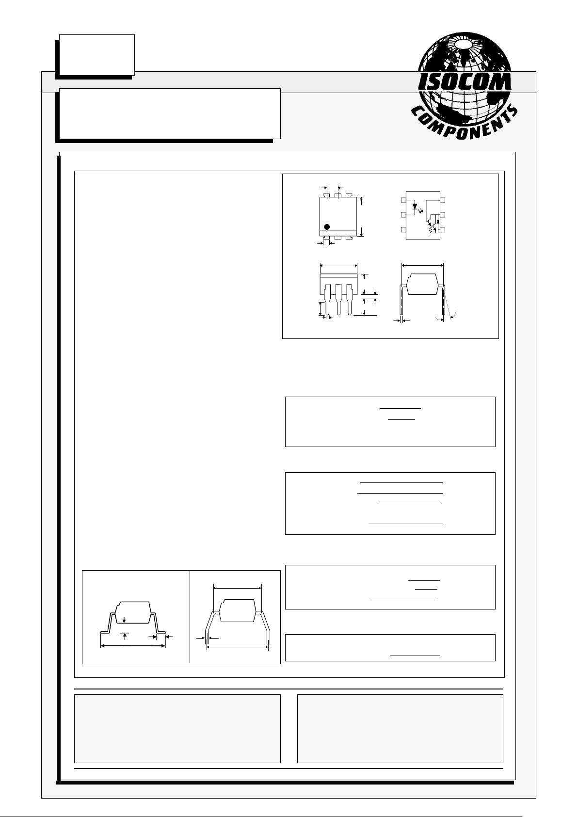
Dimensions in mm
1
3 4
6
2 5
0.5
0.26
0.5
7.0
6.0
1.2
7.62
3.0
13°
Max
3.35
4.0
3.0
2.54
7.62
6.62
ISOCOM INC
1024 S. Greenville Ave, Suite 240,
Allen, TX 75002 USA
Tel: (214) 495-0755 Fax: (214) 495-0901
e-mail info@isocom.com
http://www.isocom.com
OPTION G
7.62
SURFACE MOUNT
OPTION SM
10.16
0.26
10.46
9.86
0.6
0.1
1.25
0.75
Page 2
DB91024m-AAS/A1
11/12/00
PARAMETER MIN TYP MAX UNITS TEST CONDITION
Input Forward Voltage (VF) 1.2 1.5 V IF = 10mA
Reverse Voltage (VR) 6 V IR = 10µA
Reverse Current (IR) 10 µA VR = 6V
Output Output Breakdown Voltage ( pin 5 - 4) 55 V I54 = 1mA
Base Breakdown ( pin 4 - 6 ) 7 V IE = 0.1mA
Logic High Output 100 µA V54 = 18V
Coupled DC Current Transfer Ratio ( CTR )
IS4N46 350 % 0.5mA IF , 1V V
CE
IS4N46 500 % 1mA IF , 1V V
CE
IS4N45 250 % 1mA IF , 1V V
CE
IS4N46, IS4N45 200 % 10mA IF , 1.2V V
CE
Logic Low Output Voltage ( VOL )
IS4N46 1.0 V 0.5mA IF , 1.75mA I
OL
IS4N46 1.0 V 1mA IF , 5mA I
OL
IS4N45 1.0 V 1mA IF , 2.5mA I
OL
IS4N46, IS4N45 1.2 V 10mA IF , 20mA I
OL
Input to Output Isolation Voltage V
ISO
5300 V
RMS
See note 1
7500 V
PK
See note 1
Input-output Isolation Resistance R
ISO
10
11
Ω V
IO
= 500V (note 1)
Input-output Capacitance Cf 0.5 pF V = 0, f =1MHz
ELECTRICAL CHARACTERISTICS ( TA= 25°C Unless otherwise noted )
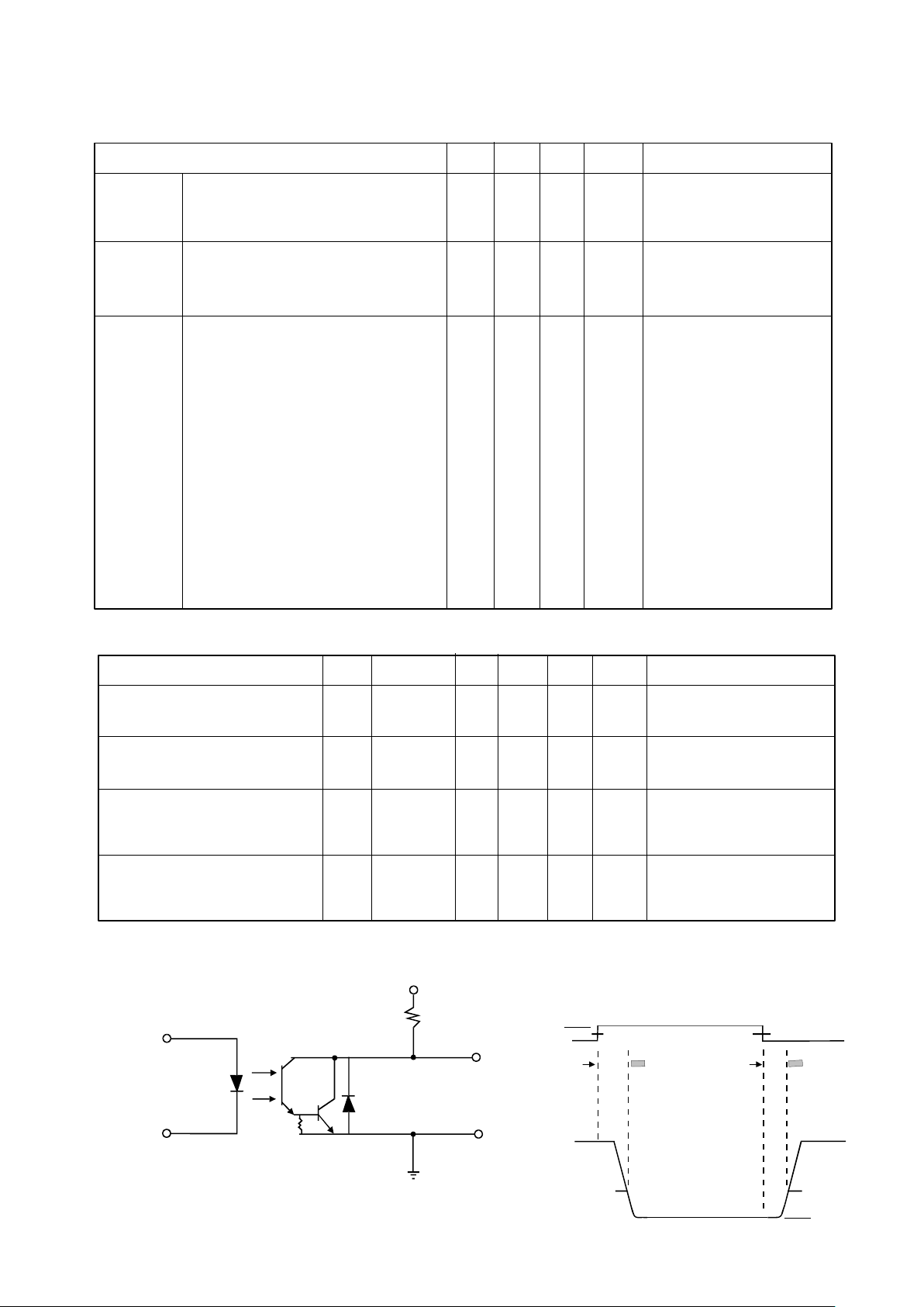
Output
V
CC
Input
FIGURE 1
R
L
SWITCHING SPECIFICATIONS AT TA = 25°C ( VCC = 5V Unless otherwise noted )
PARAMETER SYM DEVICE MIN TYP MAX UNITS TEST CONDITION
Propagation Delay Time t
PHL
IS4N46,45 80 µs IF = 1mA, RL = 10kΩ
to Logic Low at Output ( fig.1) t
PHL
IS4N46,45 5 50 µs IF = 10mA, RL = 220Ω
Propagation Delay Time t
PLH
IS4N46,45 1500 µs IF = 1mA, RL = 10kΩ
to Logic High at Output( fig.1) t
PLH
IS4N46,45 150 500 µs IF = 10mA, RL = 220Ω
Common Mode Transient
Immunity at Logic High CM
H
500 V/µs IF = 0mA,V
CM
= 10V
PP
Level Output RL = 10kΩ
Common Mode Transient
Immunity at Logic Low CM
L
500 V/µs IF= 1mA,VCM= 10V
PP
Level Output RL = 10kΩ
t
PHL
t
PLH
I
F
0
V
O
V
O
2.5V
2.5V
V
OL
5V
Page 3

DB91024m-AAS/A1
11/12/00
0 1 2 3 4 5 6
0.01
0.1
Collector-emitter voltage V
CE
( V )
-30 0 25 50 75 100
Ambient temperature TA ( °C )
Normalized Output Current vs.
Collector-emitter Voltage
Collector dark current I
CEO
(nA)
Collector Dark Current vs.
Ambient Temperature
-30 0 25 50 75 100 125
Ambient temperature TA ( °C )
100
0
Collector power dissipation P
C
(mW)
Collector Power Dissipation vs. Ambient Temperature
50
0.1 1.0 10 100
Input current IF (mA)
Normalized Output Current vs.
Input Current
0.01
0.1
1.0
10
1.0
10
100
Normalized output current
IF = 1mA
10mA
50mA
1
10
100
1k
10k
100k
150
200
250
1.0
Normalized output current
Normalized Output Current vs.
Ambient Temperature
10
-50 -25 0 25 50 75 100
Ambient temperature TA ( °C )
Ambient temperature TA ( °C )
60
30
20
10
0
40
50
-30 0 25 50 75 100 125
Forward Current vs. Ambient Temperature
Forward current I
F
(mA)
70
80
Normalized to
IF = 1mA
(300µs pulse),
V
CE
= 5V
10mA
IF = 1mA
50mA
Normalized to
IF = 1mA
(300µs pulse),
V
CE
= 5V
TA = 25 °C
0.01
Normalized output current
50V
V
CE
V
CE
= 5V
0.1
100
100
Normalized to
IF = 1mA
(300µs pulse),
V
CE
= 5V
TA = 25 °C
10V
V
CE
 Loading...