

Page 1
IS485/IS486
IS485/IS486
Bulit-in Amp. Type
OPIC Light Detector
■ Features
1. Built-in schmidt trigger circuit
2. High sensitivity (E
)
25˚C
: MAX. 35rx at Ta=
V
3. A wide range of operating supply voltage
(V
: 4.5 to 17V
CC
)
4. LSTTL and TTL compatible output
5. Low level output under incident light
(IS485
)
High level output under incident light
(IS486
)
6. Compact package
■ Applications
1. Floppy disk drive units
2. Copiers, printers, facsimiles
3. VCRs, cassette decks
4. Automatic vending machines
R0.5
+
- 0.1
15kΩ
2.6
0.3
(
Unit:mm
MAX.
Gate burr
2- 0.8
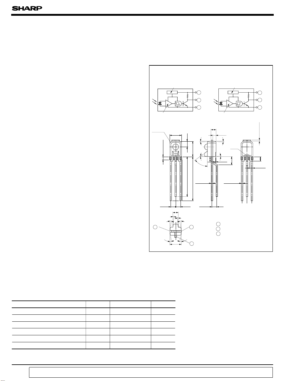
■ Outline Dimensions
Internal connection diagram
IS485 IS486
Voltage regulator
15kΩ
Amp.
2-C0.5
3.0
MAX.
0.8
Rugged resin
1.27
1.6
6˚
6˚
13
6˚
2.8
* “OPIC ”(Optical IC) is a trademark of the SHARP Corporation.
An OPIC consists of a light-detecting element and signal processing circuit integrated onto a single chip.
* Unspecified tolerance shall be ±0.2mm.
3
2
1
1.5
4.0
60˚
1.0
±
1.5-1.0
3-0.4
+
16.5
18.0
1.27
1.27
6˚
6˚
6˚
2
4˚
4˚
+ 0.3
- 0.1
Voltage regulator
Amp.
1.15
0.75
4˚
4˚
0.15
1.6
3 -0.45
1 GND
2 V
3 V
O
CC
)
3
2
1
0.3
1.4
■ Absolute Maximum Ratings
(
Ta= 25˚C
Parameter Symbol Rating Unit
Supply voltage
Output current
Power dissipation
Operating temperature
Storage temperature
*1
Soldering temperature
*1 For 5 seconds at the position of 1.4mm from the bottom face of package.
“ In the absence of confirmation by device specification sheets, SHARP takes no responsibility for any defects that occur in equipment using any of SHARP's devices, shown in catalogs,
data books, etc. Contact SHARP in order to obtain the latest version of the device specification sheets before using any SHARP's device.”
V
CC
Io 50 mA
P 175 mW
T
opr
T
stg
T
sol
-0.5 to + 17 V
-25 to + 85 ˚C
-40 to + 100 ˚C
260 ˚C
)
Page 2
IS485/IS486
■ Electro-optical Characteristics
(
Unless otherwise specified Ta= 0 to 70˚C, Vcc= 5V
Parameter Symbol Conditions MIN. TYP. MAX. Unit
Low level output voltage V
High level output voltage V
Low level supply current I
High level supply current I
*4
““High”→ Low”
threshold illuminance
*5
““Low”→ High”
threshold illuminance
*6
Hysteresis
““High”→ Low”
propagation delay time
Response
time
““Low”→ High”
propagation delay time
IS485
IS486
IS485
IS486
IS485 E
IS486 E
IS485
IS486
IS485
IS486
Rise time t
Fall time t
*2 Defines E
*3 Defines E
*4 E
represents illuminance by CIE standard light source A (tungsten lamp) when output changes from high
VHL
to low.
*5 E
represents illuminance by CIE standard light source A (tungsten lamp) when output changes from low
VLH
to high.
*6 Hysteresis stands for E
(
IS485) and EV=0 (IS486).
x
= 50l
V
=0 (IS485) and E
V
VLH/EVHL
(
IS486).
x
= 50l
V
(IS485) and E
E
E
VLH/EVHL
VHL/EVLH
t
t
VHL/EVLH
OL
OH
CCL
CCH
VHL
VLH
PHL
PLH
r
f
(IS486).
IOL= 16mA, *2 - 0.15 0.4 V
*3 3.5 - - V
*2 - 1.7 3.8 mA
*3 - mA
Ta = 25˚C - 15 35
-
Ta = 25˚C 1.5 10 -
-
Ta = 25˚C 1.5 10 -
-
Ta = 25˚C - 15 35
-
Ta = 25˚C 0.50 0.65 0.90 -
Ta = 25˚C
Ev = 50lx
= 280Ω
R
L
0.7 2.2
-
-50
1--
1--
--50
-39
-515
-515
-39
- 0.1 0.5
- 0.05 0.5
)
lx
lx
µ s
■ Recommended Operating Conditions (Ta= 0 to 70˚C
)
Parameter Symbol MIN. MAX. Unit
Supply voltage V
Low level output current I
In order to stabilize power supply line, connect a by-pass capacitor of 0.01µ F or more between V
the device.
OL
4.5 17 V
CC
-16mA
and GND near
CC
Page 3

IS485/IS486
Fig. 1 Low Level Output Current vs.
Ambient Temperature
60
)
50
mA
(
OL
40
Fig. 2 Power Dissipation vs.
Ambient Temperature
300
250
)
mW
200
(
175
30
20
Low level output voltage I
10
0
-25 -25
0 25 10050 75 85
Ambient temperature T
)
(˚C
a
Fig. 3 Relative Threshold Illuminance vs.
Supply Voltage
1.1
= 25˚C 1 E
T
a
2 E
1.0
0.9
0.8
0.7
Relative threshold illuminance
0.6
0.5
0
510 2015
(
IS485) E
VHL
(
IS486) E
VLH
1
2
(
E
IS485),
=5V
E
VLH
at V
VHL
cc
Supply voltage Vcc (V
(
IS485
VLH
(
IS486
VHL
(
IS486)=1
)
)
)
150
100
Power dissipation P
50
0
Ambient temperature Ta (˚C
Fig. 4 Low Level Output Voltage vs.
Low Level Output Current
1
)
0.5
V
(
OL
0.2
0.1
0.05
Low level output voltage V
0.02
0.01
12
Low level output current I
Fig. 5 Low Level Output Voltage vs. Fig. 6 Supply Current vs.
Ambient Temperature
0.6
Ev=50 lx (IS485
0.5
0.4
Ev=0 (IS485
)
V
(
OL
)
)
0.3
0.2
0.1
Low level output voltage V
0
-25
Ambiment temperature T
I
OL
= 30mA
7550 100250
)
(˚C
a
V
CC
16mA
5mA
=
5V
Ambient Temperature
3.0
2.5
)
2.0
mA
(
CC
1.5
1.0
0.5
Supply current I
0
-25
0255075100
Ambient temperature Ta (˚C
857550 100250
)
VCC= 5V Ta= 25˚C
E
= 50 lx (IS485
v
E
= 0 (IS486
v
20105
50 100
)
(mA
OL
V
= 17V
CC
10V
I
5V
= 17V
V
CC
10V
I
5V
)
)
)
CCL
CCH
Page 4

IS485/IS486
Fig. 7 Propagation Delay Time vs.
Illuminance
12
VCC=5V
11
)
(
µ s
, t
PHL
PLH
10
9
8
7
= 280Ω
R
L
Ta= 25˚C
1
6
5
4
3
2
Propagation delay time t
1
0
1 t
t
100 200 300 400 500 6000
PLH
PHL
(
IS485
(
IS486
)
2 t
)
t
Illuminance E
PHL
PLH
(
(
(lx
V
IS485
IS486
2
)
)
)
Test Circuit for Response Time(IS485
Voltage regulator
V
cc
Input
tr= tf= 0.01 µ s
Zo = 50Ω
47Ω
Amp.
15kΩ
0.01µ F
)
= 5V
R
L
Output
Fig. 8 Rise Time, Fall Time vs.
Load Resistance
0.8
0.7
0.6
)
µ s
(
0.5
0.4
T
V
E
t
r
= 25˚C
a
=5V
CC
= 50 lx
V
0.3
0.2
Rise time,fall time t
0.1
0
12 5
Load resistance RL (k Ω
tf
10 20 500.1 0.2 0.5
)
Test Circuit for Response Time(IS486
Voltage regulator
Vcc= 5V
Input
tr= tf= 0.01 µ s
Zo = 50Ω
47Ω
Amp.
10kΩ
R
L
Output
0.01µ F
)
Input
Output
t
PHL
t
PLH
50%
90%
10%
(
T
a
t
f
= 25˚C
+20˚+10˚
t
r
Fig. 9 Sensitivity Diagram
-10˚- 20˚
0
100
-30˚
-40˚
-50˚
-60˚
-70˚
-80˚
-90˚
80
)
%
(
60
40
Relative sensitivity
20
0
+30˚
+40˚
+50˚
+60˚
+70˚
+80˚
+90˚
Angular displacement θ
● Please refer to the chapter “Precautions for Use.”
V
OH
1.5V
)
Input
t
PLH
Output
t
r
Fig.10 Spectral Sensitivity
100
Ta= 25˚C
90
80
)
70
%
(
60
50
40
30
Relative sensitivity
20
10
0
400 500 600 700 800 900
Wavelength λ (nm
50%
t
PHL
t
f
90%
V
OH
1.5V
V
OL
10%
1000 1100 1200 1300 1400
)
 Loading...