

Page 1

IS474
IS474
Linear Output Type OPIC
Light Detector
Features
■
1. Linear output conforming to illuminance
(50 lx to 50000 lx)
2. Conforming to required visual sensitivity characteristics
by means of built-in filter
Peak sensitivity wavelength : TYP. 550 nm
3. Not dependent on kind of light source such as
incandescent lamp and fluorescent lamp
4. Easy-to-mount holder-integral side view type
Applications
■
1. TV sets
2. CRTs of personal computers and others
Outline Dimensions
■
2.0114.0
Type number
Internal connection diagram
1.4
2-R0.3
9.0
Detector center
6.0
2.4
JAPAN
1234
PPP
* Unspecified tolerance : ± 0.2
* ( ) : Reference dimensions
* Lead pitch (P) : 1.27 (at lead root)
* Lead deflection angle θ : ± 10˚ MAX.
Production country
0.28
5.8
1.5
+ 0.1
2-0.5
2-1.0
13
16.7± 0.1
- 0.2
1.7
0.5 2.0
1.0
2.0
4.5
2.0
2.75
2.54
(Unit : mm)
θθ
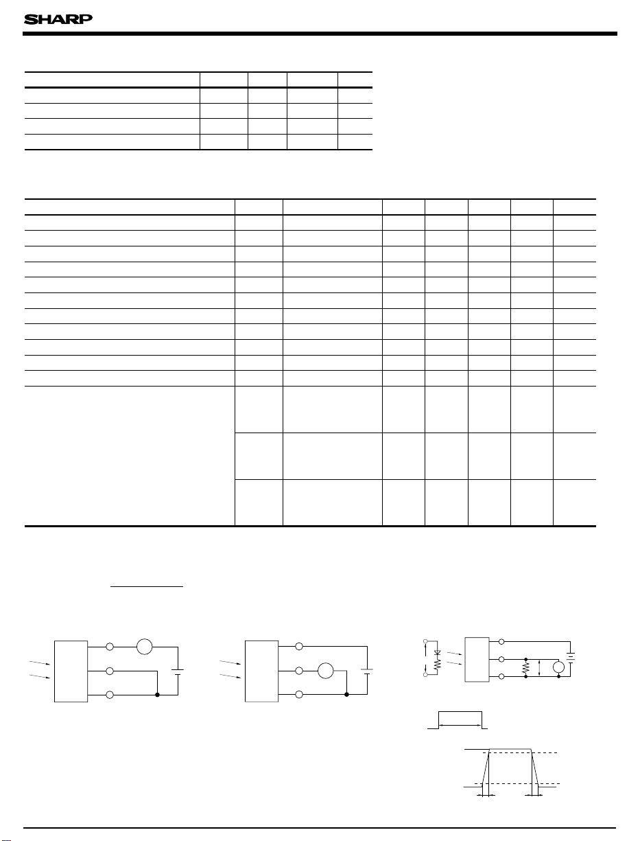
1
Constant voltage circuit
Photodiode A
2
Photodiode B
Current amp.
3
1 Vcc
3 GND 4 NC
* OPIC (Optical IC) is a trademark of SHARP corporation. An OPIC consists of
a light-detecting element and signal-processing circuit integrated onto a single chip.
2 Io
1.5
4-0.4
+0.2
- 0.1
■
Absolute Maximum Ratings
(Ta=25˚C)
Parameter Symbol Rating Unit
Supply voltage
Output current
Output voltage
V
I
V
Power dissipation
Operating temperature
Storage temperature
*1
Soldering temperature
*1 For MAX. 3 seconds at the position shown in the right drawing
“ In the absence of confirmation by device specification sheets, SHARP takes no responsibility for any defects that occur in equipment using any of SHARP's devices, shown in catalogs,
data books, etc. Contact SHARP in order to obtain the latest version of the device specification sheets before using any SHARP's device.”
T
T
T
-0.5 to 8
CC
O
O
-10
- 0.5 to V
P 150 mW
-25to +85
opr
-40to +85
stg
sol
260 ˚C
V
mA
V
CC
˚C
Soldering area
˚C
Page 2
Recommended Operating Conditions
■
Parameter Symbol MIN. MAX. Unit
Supply voltage
Illuminance
Output voltage
Operating temperature
*1 CIE standard light source A (tungsten lamp)
■
Electro-optical Characteristics
V
E
V
T
4.5 5.5 V
CC
*1
100
V
0VCC-1.5 V
O
-10 70 ˚C
opr
50 000
lx
Parameter Symbol MIN. TYP. MAX. UnitConditions
Supply current
Output current 1
Output current 2
Output current ratio 1
Output current 3
Output current 4
Output current ratio 2
Dark output current
Peak sensitivity wavelength
Response time (rise)
Response time (fall)
RI
RI
Icc
I
I
I
I
Iod
λ p
O1
O2
O1
O3
O4
O2
t
r
t
f
*1
Ev= 0 lx
*1
Ev= 100 lx
*1
Ev= 1000 lx
/Io
Io
2
*2
Ev= 100 lx
*3
Ev= 100 lx
Io3/Io
*1
Ev= 0 lx
-
= 3.3kΩ
R
L
= 3.3kΩ
R
L
0.2
0.55
- 6.0
-60
1
4
9.0
(
0.9
-10
-100
10
-
-11
-
-10
)
(
)
1.1
-
-10
(
550
12
30
)
-
-
-
Ev= 0 lx
*4
Power source
fluctuation removability
PSRR1
PSRR2
= 3.3kΩ
R
L
at 10kHz
Ev= 0 lx
= 3.3kΩ
R
L
-
48
-
39
at 100kHz
Ev=1000 lx
PSRR3
= 3.3kΩ
R
L
-
11
at 10kHz
*1 Illuminance by CIE standard light source A (tungsten lamp)
*2 Illuminance by incandescent lamp
*3 Illuminance by fluorescent lamp
*4 Power source fluctuation removability PSRR is defined according to the following formula.
PSRR =201og
Vcc ripple voltage
Vo ripple voltage
Test circuit 1 Test circuit 2 Test circuit 3
Ip=660nm
Vin
tr,tf=0.01µ s
Zo=50Ω
Vin
1.0V
IS474
T
IS474
Vcc
Io
GND
A
5V
Vcc
Ev
IS474
A
Io
GND
Ev
5V
(Vcc=5V, Ta=25˚C )
Test circuit
1.0
-14
- 140
(
1.3
- 500
mA
µ A
µ A
11
-
-
-
µ A
µ A
)
nA
nm
-
µs
-
µs
-
-
dB
-
dB
-
dB
Vcc
Io
Ro
GND
3.3kΩ
T=500µ s
Adjust Vin so that Vo waveform
may be of 1.0V amplitude
1
2
2
2
2
2
3
3
-
-
-
CRT
Vo
90%
IS474
Vcc
0V
10%
tr tf
Page 3

IS474
Fig. 1 Total Power Dissipation vs.
Ambient Temperature
160
150
140
120
100
80
60
40
Total dissipation P (mW)
20
0
Ambient temperature Ta (˚C )
Fig. 3 Spectral Sensitivity
100
80
60
40
85-25
V
=5V
CC
Ta= 25˚C
Fig. 2 Output Current vs. Illuminance
10 000
1000
100
Output current Io (µ A)
10
1
1000 255075
1
10
2
10
Illuminance EV (lx
= 5V, Ta= 25˚C
V
CC
EV :
Illuminance by CIE
standard light source A
3
10
4
10
)
5
10
Fig. 4 Relative Output Current vs.
Ambient Temperature
1.3
1.2
1.1
1.0
V
=5V
CC
1000 lx (CIE
E =
V
standard light source A)
Relative sensitivity (%)
20
0
500 600 700 800 900400
Wavelength λ (nm) Ambient temperature Ta (˚C)
Fig. 5 Dark Output Current vs. Ambient
Temperature
-6
-10
-7
-10
-8
-10
-9
-10
Dark output current Iod (A)
-10
-10
-25
=5V
V
CC
EV=0
Ambient temperature Ta (˚C)
7550250 100
Relative output current
0.9
0.8
7550250 100-25
Fig. 6 Output Current vs. Supply Voltage
-110
E
=1000 lx
V
(CIE standard
light source A)
= 25˚C
T
a
-100
Output current Io ( µA)
-90
Supply voltage VCC (V
)
1002468
Page 4

Fig. 7 Output Current vs. Output Voltage
-100
-80
-60
-40
Output current Io (µ A)
-20
V
CC
(CIE standard light source A)
0
Ev = 1 000 lx
800 lx
600 lx
400 lx
200 lx
= 5V, Ta= 25˚C
Output voltage VO (V
)
IS474
Output Current vs. Output Voltage Test Circuit
V
CC
(Main detector)
(Detector
for correction)
501234
Constant voltage circuit
PD1
PD2
5V
A
V
O
I
O
GND
Fig. 8 Supply Current vs. Supply Voltage
3
T
= 25˚C
a
(CIE standard
light source A)
Ev =10 000 lx
)
2
mA
(
CC
1
1 000 lx
Supply current I
100 lx
0 10
0
510
Supply voltage VCC (V
0 lx
)
Fig. 10 Frequency Characteristics
)
(
mV
OP
1 000
100
* Ev= 1 000 lx
10
* Ev= 100 lx
Vcc =5v
Ta =25˚C
Fig. 9 Supply Current vs. Illuminance
2
10
Vcc =5V
Vo =0
(CIE standard
light source A)
)
1
10
mA
(
CC
0
10
-1
10
Supply current I
-2
10
21 345
10 10 10 10
Illuminance Ev (lx)
Frequency Characteristics Test Circuit
(Main detector)
L E D
λP=
660nm
47Ω
Constant voltage circuit
DP1
DP2
CRT
(Detector for correction)
* Incident light quantity E : Converted value of DC
component of output voltage V
O
V
V
CC
O
5V
CRT
IOV
1kΩ
GND
O
AC output voltage V
1
10 100
1
1 000 10 000 100 000
Frequency f (Hz)
Output voltage V
Time t
V
OP
Page 5

Fig. 11 Radiation Diagram (Right/Left Direction)
- 20˚ - 10˚ 0 + 10˚ + 20˚
100
- 30˚
80
Vcc= 5V
Ta = 25˚C
+30˚
Fig. 12
Radiation Diagram (Top/Bottom Direction)
-20˚ -10˚ 0 +10˚ +20˚
100
-30˚
80
Vcc= 5V
Ta = 25˚C
IS474
+30˚
- 40˚
- 50˚
- 60˚
- 70˚
- 80˚
- 90˚
60
40
Relative sensitivity (%)
20
0
+40˚
+50˚
+60˚
+70˚
+80˚
+90˚
-40˚
-50˚
-60˚
-70˚
-80˚
-90˚
60
40
Relative sensitivity (%)
20
0
Angular displacement θ Angular displacement θ
■
Precautions for Operation
(1) It is recommended to connect a capacitor between V and GND near the device in order to stabilize power supply line
L
Device
CC
Vcc
C
<= 20 mm
L
>= 0.01 µF
C
2 pieces of photodiodes are built in this device to amplify difference in collector current between them.
Radiation of even light to 2 pieces of photodiodes is recommended.
Radiation of uneven light may cause change of spectral sensitivity or starting failure of the circuit after power is supplied.
+40˚
+50˚
+60˚
+70˚
+80˚
+90˚
(2) Cleaning
• Conduct cleaning as follows.
Solvent dip cleaning : Solvent temperature of 45˚C max., dipping time : Within 3 minutes
Ultrasonic cleaning :
Elements are affected differently depending on the size of cleaning bath, ultrasonic output, time, size of PWB and mounting
method of elements. Conduct trial cleaning on actual operating conditions in advance to make sure that no problem results.
• Use following solvents only.
Solvents : Ethyl alcohol, methyl alcohol and isopropyl alcohol
(3) Soldering
Be sure to perform soldering at values within the maximum ratings. Take care so that not external force is applied to
the lead during and immediately after soldering. Do not perform reflow soldering.
Please refer to the chapter "Precautions for Use". (Page 78 to 93)
●
 Loading...