

Page 1
IS457
IS457
High Speed Response Type
OPIC Light Detector
■
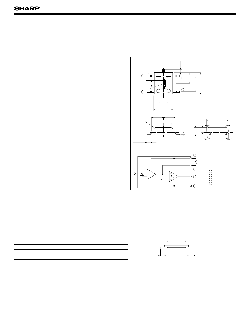
Features Outline Dimensions
1. High speed response type (t
:TYP. 300ns
PHL
)
2. Pattern with semiconductor laser spot positional deviation
(
taken into consideration
Detector size : 0.5mm x 3.0mm
3. Open collector output
4. Angle adjustment by means of outer mounting resistance
■
Applications
1. Laser beam printers
■
0.1
-
+0.2
)
* OPIC (Optical IC) is a trademark of the SHARP Corporation. An OPIC consists of
0.4
1
Detector
center
0.8
a light-detecting element and signal-processing circuit integrated onto a single chip.
3.0
2
±0.2
2.75
4.4± 0.1
+0.5
2.7
2.7
(
R0.2
+0.2
- 0.4
Internal connection diagram
-0
)
±0.1
4.4
V
REF
0.25
+0.5
- 0
0.7
+0.3
4
3
- 0
0.15
±0.2
2.5
±0.3
3.81
± 0.1
1.5
4
1
2
3
(Unit : mm)
±0.1
5.0
±0.1
5.0
10˚
1.07
10˚ 10˚
Gain resistance (Ro)
(Outer mounting)
1 R
O
2 V
O
3 GND
4 V
CC
10˚
■
Absolute Maximum Ratings
*1
Supply voltage VCC-0.5 to + 7
Parameter
High level output voltage V
Low level output voltage I
Operating temperature T
Storage temperature T
*2
Soldering temperature T
Symbol
OH
OL
opr
stg
sol
(Ta=25˚C)
Rating Unit
V
7V
40 mA
-25 to +80
-40 to +85
˚C
˚C
260 ˚C
Soldering area Soldering area
Total power dissipation P 150 mW
I
e
24 mW
5mW
60 W/cm
2
Ro terminal dissipation
*3
Incident light intensity P
*3
Radiant intensity E
*1 For 1 minute
*2 For 3 seconds at the position shown in the right drawing
*3 Max. allowable incident light intensity and radiant intensity of laser beams (λ =780 nm) to the detector
“ In the absence of confirmation by device specification sheets, SHARP takes no responsibility for any defects that occur in equipment using any of SHARP's devices, shown in catalogs,
data books, etc. Contact SHARP in order to obtain the latest version of the device specification sheets before using any SHARP's device.”
P
RO
Page 2
Electro-optical Characteristics
■
Parameter Symbol Conditions MIN. TYP. MAX. Unit
High level output voltage
Low level output voltage
High level supply current
Low level supply current
Ro terminal offset voltage =5.1kΩ
*4
"High →Low" threshold illuminance 1
*4
"High →Low" threshold illuminance 2
"High→Low" threshold incident light intensity
"High→Low" propagation delay time
Response time
"Low →High" propagation delay time
Rise time
Fall time
*4 E , E : Illuminance by CIE standard light source A (tungsten lamp) to bring about change from "High" to "Low"
VHL1 VHL2
■
Recommended Operating Conditions
I
OH
V
OL
I
CCH
I
CCL
I
OSRO
E
VHL1
E
VHL2
P
IHL
t
PHL
PLH
r
f
=51kΩ , E
R
O
IOL=40mA, E
RO=51kΩ , E
RO=51kΩ , E
R
O
=0 lx
v
=1 000 lx
V
=0 lx
V
=1 000 lx
V
RO=51kΩ 250 360 470
RO=5.1kΩ -RO=5.1kΩ , λ =780nm - 100 - µW
=15pF, Duty ratio=1:1
C
L
PI=0.2mW, λ =780nm
=5.1kΩ , RL=510Ω
R
O
Parameter Symbol MIN. MAX. Unit
Operating supply voltage
Operating temperature
Incident light intensity ( λ=780 nm)
Gain resistance
In order to stabilize power supply line, connect a by-pass capacitor of 0.1 µF between Vcc and GND
at a position within 1 cm from the lead.
V
T
P
R
4.5 5.5 V
cc
opr
I
O
060˚C
-
0.39
2.5
5.1
mW
kΩ
(
=5V, Ta = 25˚C
V
CC
- - 100 µ A
- 0.35 0.52 V
- 3.0 6.5 mA
-
5.8
-
8.6
8
mA
15
µ A
lx
4 500
lx
- 300 500 ns
- 300 500 nst
- 100 500 nst
- 50 200 nst
IS457
)
■
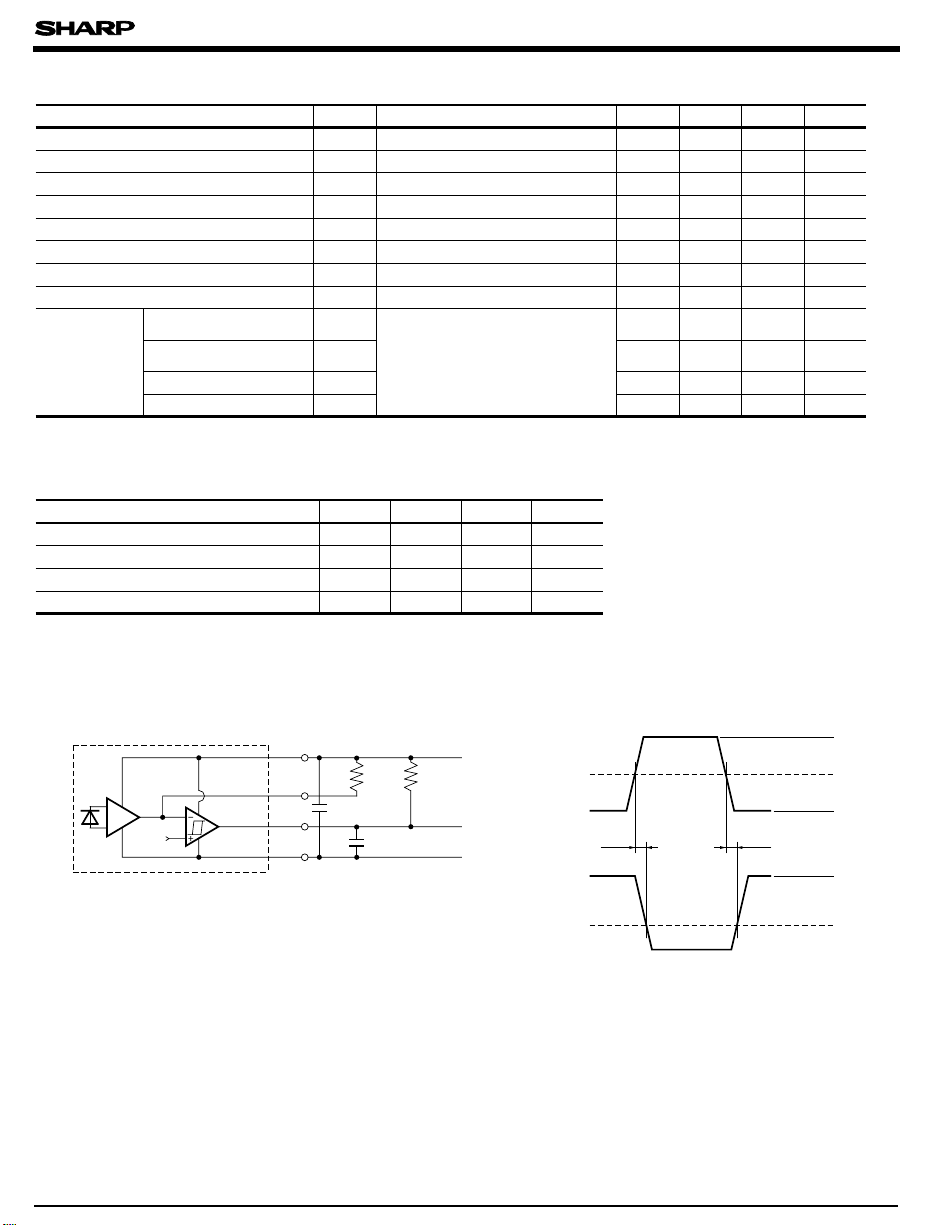
Test Circuit for Response Time
Vcc
Ro
V
ref
Notes 1. C includes the probe-to-line capacitance.
L
Vo
GND
2. Add a by-pass capacitor of 0.1µF at a position
within 1 cm from the Vcc-GND terminal.
0.1µF
5.1kΩ
C
L
510Ω
5V
Vo
GND
P
I
tt
PHL PLH
V
O
0.2mW
0.1mW
0mW
5.0V
1.5V
Page 3

IS457
Fig. 1 Total Power Dissipation vs.
Ambient Temperature
250
200
150
100
Total power dissipation P (mW)
0
Ambient temperature Ta (˚C
100755025-25500
)
Fig. 3 Low Level Output Voltage vs.
Ambient Temperature
I
OL
Vcc=5V
=40mA
0.5
)
V
(
0.4
OL
0.3
0.2
0.1
Low level output voltage V
- 25 0 25 50 75
Ambient temperature Ta (˚C)
Fig. 5 Supply Current vs. Ambient Temperature
8
7
)
6
mA
(
5
CC
4
3
2
Supply current I
1
Vcc=5V
Ro=51kΩ
Icc
IccH
L
Fig. 2 Low Level Output Voltage vs.
Low Level Output Current
0.8
)
0.7
V
(
OL
0.6
0.5
0.4
0.3
0.2
Low level output voltage V
0.1
10 20 30 40
Low level output current IOL (mA
Vcc=5V
Ta=25˚C
50 60 70
)
Fig. 4 Supply Current vs. Supply Voltage
Ta=25˚C
L
Icc
8
7
)
6
mA
(
CC
5
4
3
2
Supply current I
1
0
45678
Supply voltage VCC (V
Ro=51kΩ
IccH
)
Fig. 6 "High→Low" Threshold
Incident Light Intensity vs. Supply Voltage
200
150
)
µW
(
100
IHL
50
"High→Low" threshold incident
light intensity P
Ta=25˚C
Ro=5.1kΩ
80
-25 25 50 750
Ambient temperature Ta (˚C )
4
0
5678
Supply voltage VCC (V
)
Page 4

IS457
Fig. 7 Propagation Delay Time vs.
Ambient Temperature
)
400
ns
(
PHL
, t
300
PLH
200
100
Propagation delay time t
-25 0 25 50 75
Ambient temperature Ta (˚C )
Fig. 9 Spectral Sensitivity
100
80
60
40
t
PHL
t
PLH
Vcc=5V
Ro=5.1kΩ
R
L=510Ω
T
= 25˚C
a
Fig. 8 Rise, Fall Time vs. Ambient Temperature
Vcc=5V
160
140
)
ns
120
(
f
, t
r
100
80
60
Rise, fall time t
40
20
-25 0 25 50 75
Ambient temperature Ta (˚C )
Ro=5.1kΩ
L=510Ω
R
t
t
r
f
Relative sensitivity (%)
20
0
300 400 500 600 700 800 900
1000 1100
Wavelength λ (nm)
●
Please refer to the chapter "Precautions for Use". (Page 78 to 93)
 Loading...