

Page 1
IS456
IS456
High Speed Response Type
OPIC Light Detector
■ Features
1. High speed response (t
2. Uses a pattern to allow for possible
positional deviation of the semiconductor
laser spot.
3. Compact, mini-flat package
: TYP.230ns
PHL
■ Applications
1. Laser beam printers
■ Absolute Maximum Ratings
*1
Parameter
Supply voltage
High level output voltage
Low level output current
Operating temperature
Storage temperature
*2
Soldering temperature
Power dissipation
RO terminal power dissipation
*3
Incident light intensity
*3
Radiant intensity
*1 For 1 minute
*2 For 3 seconds at the position shown in the follow-
ing drawing.
*3 Maximum allowable incident light intensity and
radiant intensity of laser beam (λ = 780nm) to
the device.
Soldering area Soldering area
Symbol
V
CC
V
OH
I
OL
T
opr
T
stg
T
sol
P 150 mW
P
RO
P
I
E
e
■ Electro-optical Characteristics
Parameter Symbol Conditions MIN. TYP. MAX. Unit
High level output voltage V
Low level output voltage V
High level supply current I
Low level supply current I
*4
“High→Low ” threshold illuminance 1
*4
“High→Low ” threshold illuminance 2
“ High→Low ” threshold incident light intensity
“ High→Low”
propagation delay time
“ Low→High”
propagation delay time
2 represent illuminance by CIE standard light source A (tungsten lamp) when output goes from high to low.
VHL
*4 E
Response
time
1, E
VHL
)
(
Ta=25˚C
Rating Unit
-0.5 to + 7
7V
20 mA
-25 to+ 80
-40 to+ 85
260 ˚C
24
5
60
OH
OL
CCH
CCL
E
VHL1
E
VHL2
P
IHL
t
PHL
t
PLH
r
f
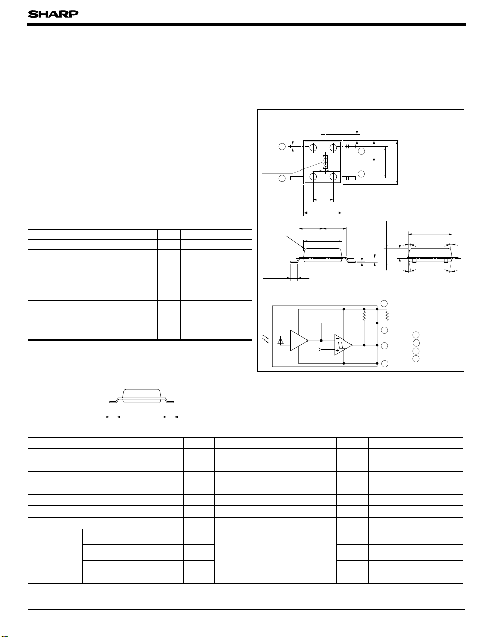
■ Outline Dimensions
0.3-0.1
+
0.4
1
Detector
center
2
V
˚C
˚C
mW
mW
WB
)
(
0.8
2.7
)
R0.2
+
0.2
-
0.4
Internal connection
diagram
V
2.75
4.4± 0.1
+
0.5
-
0
4.4
REF
±
2.7
± 0.1
0.2
0.25
+
-
(
Unit :mm
0.2
±
0.7
2.5
4
0.3
0.1
±
±
5.0
3.81
3
0.5
0
+
0.3-0
0.15
0.3-0.2
+
0.5
0.1
±
4
1
2
3
1.07
1.5
Gain resistor(Ro
(
Outer mounting
±
5.0
10˚
10˚ 10˚
1 R
O
2 V
O
3 GND
4 V
CC
)
0.1
10˚
)
)
*“OPIC” (Optical IC) is a trademark of the SHARP Corporation.
An OPIC consists of a light-detecting element and signal processing circuit integrated onto a single chip.
)
R
=51kΩ , E
O
IOL=10mA, E
=0
V
=1 000lx
V
(
= 5V, Ta= 25˚C
V
CC
4.9 - - V
- 0.4 0.6 V
RO=51kΩ , EV=0 - 2.6 4.5 mA
RO=51kΩ , E
RO=51kΩ 330 470 600
RO=5.1kΩ --
=1 000lx
V
- 3.8 6.6 mA
lx
5 800
lx
RO=5.1kΩ , l =780nm - 100 - µW
=15pF, Duty=1: 1
C
L
PI=0.2mW, λ =780nm
RO=5.1kΩ , RL=510Ω
- 230 400 ns
- 230 400 ns
- 60 200 ns Rise time t
- 20 100 ns Fall time t
“ In the absence of confirmation by device specification sheets, SHARP takes no responsibility for any defects that occur in equipment using any of SHARP's devices, shown in catalogs,
data books, etc. Contact SHARP in order to obtain the latest version of the device specification sheets before using any SHARP's device.”
Page 2
■ Recommended Operating Conditions
Parameter Symbol MIN. MAX. Unit
Operating supply voltage V
Operating temperature T
Incident light intentity (λ = 780nm
In order to stabilize power supply line, connect a by-pass capacitor of 0.1µF
between Vcc and GND near the device.
)
P
4.5 5.5 V
cc
opr
I
060˚C
- 2.5 mW
IS456
Fig. 1 Total Power Dissipation vs.
Ambient Temperature
250
)
200
mW
(
150
100
Total power dissipation P
0
Ambient temperature Ta (˚C
)
Fig. 3 Low Level Output Voltage vs.
Ambient Temperature
0.6
0.5
)
mA
(
0.4
OL
0.3
0.2
0.1
Low level output voltage V
0
025
Ambient temperature T
VCC=5V
I
= 20mA
OL
10mA
50
75 100-25 3
)
(˚C
a
Fig. 2 Low Level Output Voltage vs.
Low Level Output Current
10
5
)
V
(
OL
2
1
0.5
0.2
Low level output voltage V
1
100755025-25500
11052
Low level output Current IOL (mA
VCC=5V
T
= 25˚C
a
)
1005020
Fig. 4 Supply Current vs. Supply Voltage
6
5
)
mA
4
(
CC
3
2
Supply current I
1
0
Supply voltage VCC (V
Ta= 25˚C
I
CCL
I
CCH
)
87654
Page 3

IS456
Fig. 5 Supply Current vs.
Ambient Temperature
6
VCC= 5.0V
)
4
mA
(
CC
2
I
CCL
I
CCH
Supply current I
0
0-25
25 50 75 100 01234567
Ambient temperature Ta (˚C
)
Fig. 7 “High→Low” Threshold Incident Light
Intensity vs. Ambient Temperature
a
(˚C
VCC= 5.0V
= 5.1kΩ
R
O
)
80
140
)
120
µ W
(
IHL
100
light intensity P
“High→Low” threshold incident
80
0
-25 25 50 75
0
Ambient temperature T
Fig. 9 Propagation Delay Time vs.
Incident Light Intensity
250
)
200
ns
(
PHL
, t
150
PLH
100
50
Propagation delay time t
0
0.5
0.2
Incident light intensity P
R
O
t
PLH
(mW
I
VCC= 5.0V
R
= 510Ω
L
T
= 25˚C
a
RO: Dotted line
t
PHL
)
2.52.01.51.00
Fig. 6 “High→Low” Threshold Incident Light
Intensity vs. Gain Resistanse
2000
1000
)
500
µ W
(
200
IHL
V
T
=5V
CC
= 25˚C
a
100
50
20
“High→Low” threshold
incident light intensity P
10
Gain resistance RO (k Ω
)
Fig. 8 “High→Low” Threshold Incident Light
Intensity vs. Supply Voltage
200
Ta= 25˚C
= 5.1kΩ
R
O
150
)
µ W
(
100
IHL
50
“High→Low” threshold incident
light intensity P
0
3
4
5678
Supply voltage VCC (V
)
Fig.10 Propagation Delay Time vs.
Gain Resistance
500
)
ns
400
(
PHL
, t
300
PLH
200
100
Propagation delay time t
0
0
Gain resistance R
VCC= 5V, PI= 0.6mW
R
= 510kΩ , Ta= 25˚C
L
t
PLH
t
PHL
)
(kΩ
O
654321
Page 4

IS456
Fig.11 Propagation Delay Time vs.
Ambient Temperature
400
VCC= 5V, RO=5.1KΩ
R
= 510Ω
L
)
ns
(
300
PHL
, t
PLH
200
t
PHL
t
PLH
t
PLH
t
PHL
100
Propagation delay time t
0
Ambient temperature Ta (˚C
)
Fig.13 Rise Time, Fall Time vs.
Ambient Temperature
100
VCC= 5V, RO= 5.1KΩ
= 510Ω
R
L
80
)
ns
(
f
, t
60
r
40
20
Rise time, fall time t
t
r
t
f
Fig.12 Rise Time, Fall Time vs.
Load Resistance
300
Ta= 25˚C
=5V
V
CC
250
)
ns
(
200
f
, t
r
t
r
150
100
Rise time, fall time t
50
t
100755025-25 0
0
0123456
Load resistance RL (K Ω
f
)
Fig.14 Spectral Sensitivity
100
80
)
%
(
60
40
Relative sensitivity
20
T
a
= 25˚C
0
Ambient temperature T
a
(˚C
0
100755025-25 0
)
300 400 500 600 700 800 900
Wavelength λ (nm
1000 1100
)
Page 5

Test Circuit for Response Time
IS456
Constant
current
Laser
diode
V
Incident
light
intensity
t
PHL
Output
t
f
● Please refer to the chapter “Precautions for Use.”
VCC= 5V
5.1
510Ω
kΩ
0.1µ F
ref
C
L
Output
0.2mW
0.1mW
t
PLH
0mW
90%
1.5V
10%
t
r
 Loading...