

Datasheet IS41LV32256-35TQ, IS41LV32256-35PQ, IS41LV32256-30TQ, IS41LV32256-30PQ, IS41LV32256-28TQ Datasheet (ISSI)
...Page 1

IS41LV32256 ISSI
256K x 32 (8-Mbit) EDO DYNAMIC RAM
SEPTEMBER 2000
3.3V, 100/83/66 MHz
®
FEATURES
• 262,144-word by 32-bit organization
• Single +3.3V ± 0.3V power supply
• Four CAS inputs for Byte Write and Byte Read
control
• Refresh modes: RAS-Only, CAS-Before-RAS (CBR),
and Hidden
• 512-cycle refresh in 8 ms
• Fast Page Mode with Extended Data Out
• 100-pin PQFP, TQFP package
DESCRIPTION
The ISSI IS41LV32256 is organized in a 262,122 x 32-bit
CMOS Dynamic Random Access Memory. Four CAS signals
facilitate execution of Byte Read and Byte Write operations.
A very fast EDO cycle time of 10 ns allows an operating
frequency of 100 MHz and makes the IS41LV32256 an ideal
frame buffer memory for graphics applications.
The IS41LV32256 is compatible with JEDEC standard
SGRAMs. This 8-Mbit EDO memory offers a significantly
lower latency and a faster memory cycle than the SGRAM.
ISSI's IS41LV32256 3.3V 256K x 32 device is pin/voltage
compatible with all standard SGRAM parts.
The IS41LV32256 is available in a 100-pin PQFP and TQFP
package.
KEY TIMING PARAMETERS
Parameter -28 -30 -35 Unit
Max. RAS Access Time (tRAC) 283035ns
Max. CAS Access Time (tCAC)9910ns
Max. Column Address Access Time (tAA)151618ns
Max. OE Access Time (tOE)9910ns
Min. Read/Write Cycle Time (tRC) 485360ns
Min. EDO Cycle Time (tPC) 121215ns
ISSI reserves the right to make changes to its products at any time without notice in order to improve design and supply the best possible product. We assume no responsibility for any errors
which may appear in this publication. © Copyright 2000, Integrated Silicon Solution, Inc.
Integrated Silicon Solution, Inc.
Rev. A
09/29/00
1
Page 2
IS41LV32256 ISSI
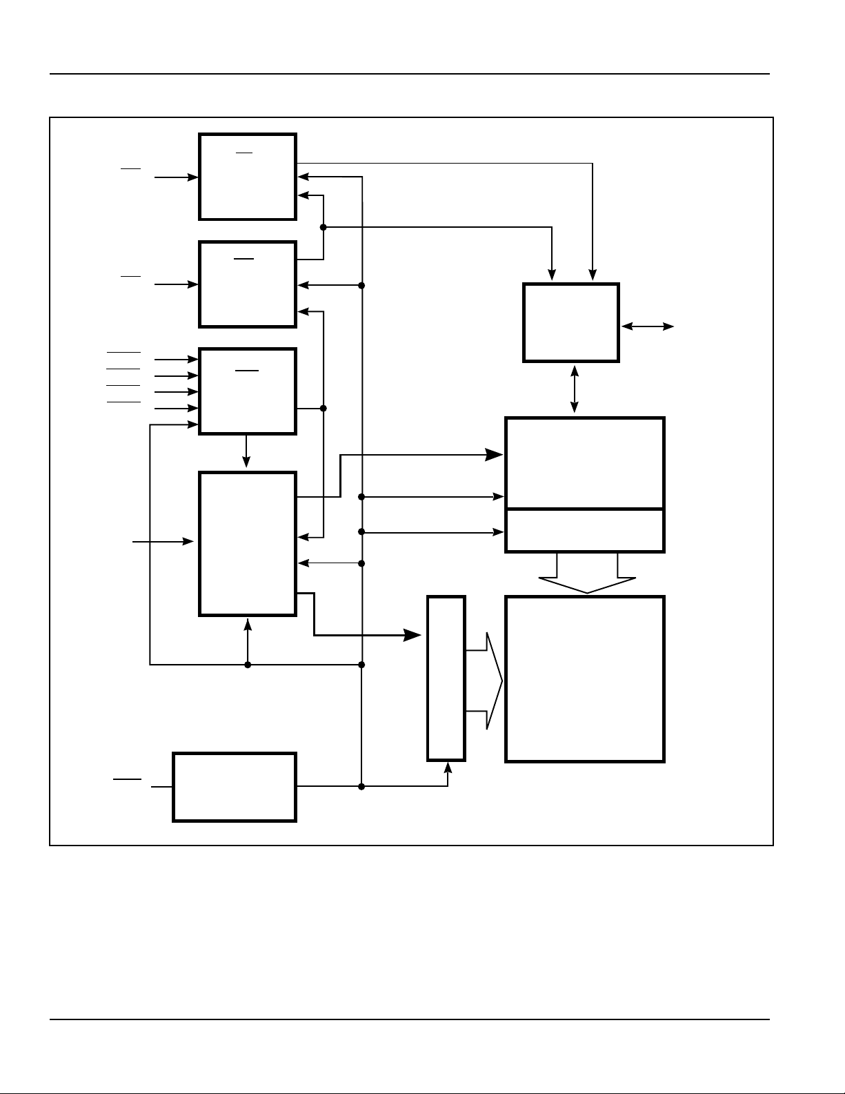
FUNCTIONAL BLOCK DIAGRAM
OE
OE
WE
CAS0
CAS1
CAS2
CAS3
CLOCK
GENERATOR
WE
CLOCK
GENERATOR
CAS
CLOCK
GENERATOR
Data I/O
Buffers
I/O0-31
®
A0-A8
RAS
CONTROLS
RAS
CLOCK
GENERATOR
AX0-AX8
AY0-AY8
512
ROW DECODERS
COLUMN DECODERS
SENSE AMPLIFIERS
512 x 32
MEMORY ARRAY
256K x 32
2
Integrated Silicon Solution, Inc.
Rev. A
09/29/00
Page 3
IS41LV32256 ISSI
3
1
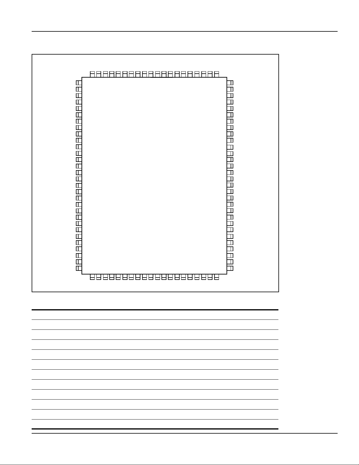
PIN CONFIGURATIONS
100-Pin PQFP, TQFP
I/O2
GND
I/O1
I/O0
VccNCNCNCNCNCNCNCNCNCNC
GND
I/O31
I/O30
GND
I/O29
®
I/O3
Vcc
I/O4
I/O5
GND
I/O6
I/O7
Vcc
I/O16
I/O17
GND
I/O18
I/O19
Vcc
Vcc
GND
I/O20
I/O21
GND
I/O22
I/O23
Vcc
CAS0
CAS2
WE
NC
NC
RAS
NC
NC
99989796959493929190898887868584838281
1
100
2
3
4
5
6
7
8
9
10
11
12
13
14
15
16
17
18
19
20
21
22
23
24
25
26
27
28
29
30
31323334353637383940414243444546474849
50
80
I/O28
79
Vcc
78
I/O27
77
I/O26
76
GND
75
I/O25
74
I/O24
73
Vcc
72
I/O15
71
I/O14
70
GND
69
I/O13
68
I/O12
67
Vcc
66
GND
65
Vcc
64
I/O11
63
I/O10
62
GND
61
I/O9
60
I/O8
59
Vcc
58
NC
57
CAS
56
CAS
55
NC
54
NC
53
OE
52
NC
51
A8
A0A1A2
A3
PIN DESCRIPTIONS
A0-A8 Address Inputs
RAS Row Address Strobe
CAS0 Column Address Strobe for First Byte (I/O0-I/O7)
CAS1 Column Address Strobe for Second Byte (I/O8-I/O15)
CAS2 Column Address Strobe for Third Byte (I/O16-I/O23)
CAS3 Column Address Strobe for Fourth Byte (I/O24-I/O31)
WE Write Enable
OE Output Enable
I/O0-I/O31 Data Inputs/Outputs
Vcc +3.3V Supply
GND Ground
NC No Connection: This pin should be left unconnected or tied to ground.
Integrated Silicon Solution, Inc.
Rev. A
09/29/00
NCNCNCNCNCNCNCNCNC
Vcc
A4A5A6
NC
GND
A7
3
Page 4

IS41LV32256 ISSI
TRUTH TABLE
Function RA S CAS0 CAS1 CAS2 CAS3 WE OE Address I/O
Standby H HHHHXX X High-Z
Read: Double Word L LLLLHLROW/COL DOUT
Read: 1st Byte L L H H H H L ROW/COL I/O0-7=DOUT;
I/O8-31=High-Z
Read: 2nd Byte L H L H H H L ROW/COL I/O0-7=High-Z;
I/O8-15=DOUT;
I/O16-31=High-Z
Read: 3rd Byte L H H L H H L ROW/COL I/O0-15=High-Z;
I/O16-23=DOUT;
I/O24-31=High-Z
Read: 4th Byte L H H H L H L ROW/COL I/O0-23=High-Z;
I/O24-31=DOUT
Write: Double Word (Early) L LLLLLXROW/COL DIN
Write: 1st Byte (Early) L L H H H L X ROW/COL I/O0-7=DIN;
I/O8-31=X
Write: 2nd Byte (Early) L H L H H L X ROW/COL I/O0-8=X;
I/O8-15=DIN;
I/O16-31=X
Write: 3rd Byte (Early) L H H L H L X ROW/COL I/O0-15=X;
I/O16-23=DIN;
I/O24-31=X
Write: 4th Byte (Early) L H H H L L X ROW/COL I/O0-23=X;
I/O24-31=DIN
Read-Write
Fast-Page-Mode Read: EDO
Fast-Page-Mode Read: High-Z
Fast-Page-Mode Write: (Early)
Fast-Page-Mode Read-Write
Hidden Refresh Read
Hidden Refresh Write
RAS-Only Refresh LHHHHXX ROW High-Z
CBR Refresh
Notes:
1. BYTE WRITE may be executed with CAS0, CAS1, CAS2 or CAS3 active.
2. BYTE READ may be executed with CAS0, CAS1, CAS2 or CAS3 active.
3. Only one CAS signal (CAS0, CAS1, CAS2 or CAS3) must be active.
(1,2)
LLLLLH∅LL∅H ROW/COL DOUT∅DIN
(2)
1st Cycle: L H∅LH∅LH∅LH∅L H L ROW/COL DOUT
Subsequent Cycles: L H∅LH∅LH∅LH∅L H L COL DOUT
(2)
1st Cycle: L H∅LH∅LH∅LH∅LHH∅L ROW/COL DOUT
Subsequent Cycles: L H∅LH∅LH∅LH∅LHH∅L COL DOUT
(1)
1st Cycle: L H∅LH∅LH∅LH∅L L X ROW/COL DIN
Subsequent Cycles: L H∅LH∅LH∅LH∅L L X COL DIN
(1,2
)
1st Cycle: L H∅LH∅LH∅LH∅LH∅LL∅ H ROW/COL DOUT∅DIN
Subsequent Cycles: L H∅LH∅LH∅LH∅LH∅LL∅ H COL DOUT∅DIN
(2)
(1)
(3)
L∅H∅LLLLLHLROW/COL DOUT
L∅H∅LLLLLLXROW/COLDIN∅High-Z
H∅LLLLLXX X High-Z
®
4
Integrated Silicon Solution, Inc.
Rev. A
09/29/00
Page 5

IS41LV32256 ISSI
POWER-ON
The initial application of the VCC supply requires a 200-µs
wait followed by a minimum of any eight initialization
cycles containing a RAS clock. During Power-On, the VCC
current is dependent on the input levels of RAS and CAS.
It is recommended that RAS and CAS track with VCC or be
held at a valid VIH during Power-On to avoid current
surges.
®
ABSOLUTE MAXIMUM RATINGS
(1)
Symbol Parameters Rating Unit
tA Ambient Temperature Under Bias –1.0 to +80 °C
tSTG Storage Temperature –50 to +125 °C
VT Voltage Relative to GND –1.0 to +5.5 V
IOUT Data Output Current 50 mA
PD Power Dissipation 1.0 W
Note:
1. Stress greater than those listed under ABSOLUTE MAXIMUM RATINGS may cause permanent
damage to the device. This is a stress rating only and functional operation of the device at these
or any other conditions above those indicated in the operational sections of this specification is
not implied. Exposure to absolute maximum rating conditions for extended periods may affect
reliability.
RECOMMENDED OPERATING CONDITIONS
(1)
(TA = 0°C to 70°C)
Symbol Parameter Min. Typ. Max. Unit
VCC Power Supply 3.0 3.3 3.6 V
VIH Input High Voltage 2.4 — VCC + 0.5 V
VIL Input Low Voltage –0.5 — 0.4 V
Note:
1. Voltages are referenced to GND.
CAPACITANCE
(1,2)
Symbol Parameter Max. Unit
CIN Input Capacitance 5 pF
CIO Data Input/Output Capacitance 7 pF
Notes:
1. Capacitance is sampled and 100% tested.
2. Test conditions: TA = 25°C, f = 1 MHz, VCC = 3.3V.
Integrated Silicon Solution, Inc.
Rev. A
09/29/00
5
Page 6

IS41LV32256 ISSI
DC CHARACTERISTICS (TA = 0°C to 70°C, VCC = 3.3V ± 0.3V)
-28 -30 -35
Symbol Parameter Condition Min. Max. Min. Max. Min. Max. Units
VIH Input HIGH (Logic 1) Voltage, All Inputs — 2.0 Vcc + 0.5 2.0 Vcc + 0.5 2.0 Vcc + 0.5 V
VIL Input LOW (Logic 1) Voltage, All Inputs —–0.5 0.8 –0.5 0.8 –0.5 0.8 V
VOH Output HIGH Voltage IOH = –2 mA 2.4 Vcc 2.4 Vcc 2.4 Vcc V
VOL Output LOW Voltage IOL = 2 mA 00.4 00.4 00.4 V
ILI Input Leakage Current 0V < VIN < VCC –10 10 –10 10 –10 10 µA
I
LO Output Leakage Current 0V < VOUT < 3.6V; –10 10 –10 10 –10 10 µA
Output Disable
ICC1 Average Power Supply Current RAS, CAS Cycling; — 250 — 250 — 240 mA
(Operating)
ICC2 Power Supply Current (Standby) RAS, CAS = VIH — 2.5 — 2.5 — 2.5 mA
Icc3 Average Power Supply Current RAS = Cycling; — 250 — 250 — 240 mA
(RAS-Only Refresh)
ICC4 Average Power Supply Current RAS = VIL; — 230 — 230 — 220 mA
(Fast Page Mode)
ICC5 Average Power Supply Current RAS = Cycling; — 250 — 250 — 240 mA
(CAS-before-RAS Refresh)
ICC6 CMOS Standby Current RAS, CAS = VCC –0.2V — 600 — 600 — 600 µA
(2,3,15,16)
(2,3,15,16)
(2,3,15,18)
(2,3,15.16)
tRC = Min.
CAS = VIH; tRC = Min.
CAS = Cycling; tPC = Min.
CAS-before-RAS
®
AC CHARACTERISTICS
(1,2,3,4,5,6)
(Recommended Operating Conditions unless otherwise noted.)
-28 -30 -35
Symbol Parameter Min. Max. Min. Max. Min. Max. Units
tRC Random READ or WRITE Cycle Time 48 — 53 — 60 — ns
tRAC Access Time from RAS
tCAC Access Time from CAS
tAA Access Time from Column-Address
(6, 7)
(6, 8, 15)
— 28 — 30 — 35 ns
— 9 — 9 — 10 ns
(6)
— 15 — 16 — 18 ns
tRAS RAS Pulse Width 28 10K 30 10K 35 10K ns
tRP RAS Precharge Time 17 — 18 — 20 — ns
(21)
(26)
(9, 25)
(10, 20)
5 10K 5 10K 6 10K ns
5 — 5 — 5 — ns
28 — 30 — 35 — ns
10 19 10 21 11 28 ns
tCAS CAS Pulse Width
tCP CAS Precharge Time
tCSH CAS Hold Time
tRCD RAS to CAS Delay Time
tASR Row-Address Setup Time 0 — 0 — 0 — ns
tRAH Row-Address Hold Time 6 — 6 — 7 — ns
(20)
(20)
0 — 0 — 0 — ns
5 — 5 — 6 — ns
tASC Column-Address Setup Time
tCAH Column-Address Hold Time
tAR Column-Address Hold Time 21 — 22 — 25 — ns
(referenced to RAS)
tRAD RAS to Column-Address Delay Time
(11)
813 815 916 ns
tRAL Column-Address to RAS Lead Time 15 — 16 — 18 — ns
tRPC RAS to CAS Precharge Time 0 — 0 — 0 — ns
tRSH RAS Hold Time
(27)
7 — 7 — 8 — ns
(Continued)
6
Integrated Silicon Solution, Inc.
Rev. A
09/29/00
Page 7

IS41LV32256 ISSI
®
AC CHARACTERISTICS
(1,2,3,4,5,6)
(Recommended Operating Conditions unless otherwise noted.)
-28 -30 -35
Symbol Parameter Min. Max. Min. Max. Min. Max. Units
tCLZ CAS to Output in Low-Z
tCRP CAS to RAS Precharge Time
tOD Output Disable Time
tOE Output Enable Time
(15, 29)
(19, 28, 29)
(15, 16)
(21)
3 — 3 — 3 — ns
5 — 5 — 5 — ns
315 315 315 ns
— 9 — 9 — 10 ns
tOEHC OE HIGH Hold Time from CAS HIGH 10 — 10 — 10 — ns
tOEP OE HIGH Pulse Width 10 — 10 — 10 — ns
tOES OE LOW to CAS HIGH Setup Time 5 — 5 — 5 — ns
tRCS Read Command Setup Time
(17, 20)
0 — 0 — 0 — ns
tRRH Read Command Hold Time 0 — 0 — 0 — ns
(referenced to RAS)
(12)
tRCH Read Command Hold Time 0 — 0 — 0 — ns
(referenced to CAS)
tWCH Write Command Hold Time
(12, 17, 21)
(17, 27)
5 — 5 — 5 — ns
tWCR Write Command Hold Time 21 — 22 — 24 — ns
(referenced to RAS)
tWP Write Command Pulse Width
(17)
(17)
5 — 5 — 6 — ns
tWPZ WE Pulse Widths to Disable Outputs 10 — 10 — 10 — ns
(14, 17, 20)
(17)
(17, 21)
7 — 7 — 8 — ns
5 — 5 — 8 — ns
0 — 0 — 0 — ns
tRWL Write Command to RAS Lead Time
tCWL Write Command to CAS Lead Time
tWCS Write Command Setup Time
tDHR Data-in Hold Time (referenced to RAS)21 — 22 — 24 — ns
tACH Column-Address Setup Time to CAS 15 — 15 — 15 — ns
Precharge during WRITE Cycle
tOEH OE Hold Time from WE during 5 — 5 — 6 — ns
READ-MODIFY-WRITE cycle
tDS Data-In Setup Time
tDH Data-In Hold Time
(15, 22)
(15, 22)
(18)
0 — 0 — 0 — ns
5 — 5 — 6 — ns
tRWC READ-MODIFY-WRITE Cycle Time 73 — 73 — 80 — ns
tRWD RAS to WE Delay Time during 40 — 40 — 45 — ns
READ-MODIFY-WRITE Cycle
tCWD CAS to WE Delay Time
(14, 20)
tAWD Column-Address to WE Delay Time
(14)
(14)
18 — 18 — 20 — ns
24 — 25 — 30 — ns
tPC EDO Page Mode READ or WRITE 12 — 12 — 15 — ns
Cycle Time
(24)
tRASP RAS Pulse Width in EDO Page Mode 28 100K 30 100K 35 100K ns
tCPA Access Time from CAS Precharge
(15)
— 17 — 18 — 21 ns
tPRWC EDO Page Mode READ-WRITE 34 — 35 — 40 — ns
Cycle Time
(24)
tCHO Data Output Hold after CAS LOW 3 — 3 — 3 — ns
tOFF Output Buffer Turn-Off Delay from 3 7 3 7 3 15 ns
CAS or RAS
(13,15,19, 29)
tWHZ Output Disable Delay from WE 310 310 315 ns
(Continued)
Integrated Silicon Solution, Inc.
Rev. A
09/29/00
7
Page 8

IS41LV32256 ISSI
®
AC CHARACTERISTICS
(1,2,3,4,5,6)
(Recommended Operating Conditions unless otherwise noted.)
-28 -30 -35
Symbol Parameter Min. Max. Min. Max. Min. Max. Units
tCLCH Last CAS going LOW to First CAS 10 — 10 — 10 — ns
returning HIGH
tCSR CAS Setup Time (CBR REFRESH)
tCHR CAS Hold Time (CBR REFRESH)
(23)
(30, 20)
(30, 21)
5 — 5 — 8 — ns
7 — 7 — 8 — ns
tORD OE Setup Time prior to RAS during 0 — 0 — 0 — ns
HIDDEN REFRESH Cycle
tREF Refresh Period (512 Cycles) — 8 — 8 — 8ms
tT Transition Time (Rise or Fall)
Notes:
1. An initial pause of 200 µs is required after power-up followed by eight RAS refresh cycle (RAS-Only or CBR) before proper device
operation is assured. The eight RAS cycles wake-up should be repeated any time the t
2. VIH (MIN) and VIL (MAX) are reference levels for measuring timing of input signals. Transition times, are measured between VIH and
IL (or between VIL and VIH) and assume to be 1 ns for all inputs.
V
3. In addition to meeting the transition rate specification, all input signals must transit between V
in a monotonic manner.
4. If CAS and RAS = V
5. If CAS = V
IL, data output may contain data from the last valid READ cycle.
6. Measured with a load equivalent to one TTL gate and 50 pF.
7. Assumes that t
the amount that t
8. Assumes that tRCD • tRCD (MAX).
9. If CAS is LOW at the falling edge of RAS, data out will be maintained from the previous cycle. To initiate a new cycle and clear the
data output buffer, CAS and RAS must be pulsed for t
10. Operation with the tRCD (MAX) limit ensures that tRAC (MAX) can be met. tRCD (MAX) is specified as a reference point only; if tRCD
is greater than the specified tRCD (MAX) limit, access time is controlled exclusively by tCAC.
11. Operation within the t
is greater than the specified tRAD (MAX) limit, access time is controlled exclusively by tAA.
12. Either t
13. t
RCH or tRRH must be satisfied for a READ cycle.
OFF (MAX) defines the time at which the output achieves the open circuit condition; it is not a reference to VOH or VOL.
14. tWCS, tRWD, tAWD and tCWD are restrictive operating parameters in LATE WRITE and READ-MODIFY-WRITE cycle only. If tWCS • tWCS
(MIN), the cycle is an EARLY WRITE cycle and the data output will remain open circuit throughout the entire cycle. If tRWD • tRWD
(MIN), tAWD • tAWD (MIN) and tCWD • tCWD (MIN), the cycle is a READ-WRITE cycle and the data output will contain data read from
the selected cell. If neither of the above conditions is met, the state of I/O (at access time and until CAS and RAS or OE go back
IH) is indeterminate. OE held HIGH and WE taken LOW after CAS goes LOW result in a LATE WRITE (OE-controlled) cycle.
to V
15. Output parameter (I/O) is referenced to corresponding CAS input, I/O0-I/O7 by LCAS and I/O8-I/O15 by UCAS.
16. During a READ cycle, if OE is LOW then taken HIGH before CAS goes HIGH, I/O goes open. If OE is tied permanently LOW, a LATE
WRITE or READ-MODIFY-WRITE is not possible.
17. Write command is defined as WE going low.
18. LATE WRITE and READ-MODIFY-WRITE cycles must have both t
that the output buffers will be open during the WRITE cycle. The I/Os will provide the previously written data if CAS remains LOW
and OE is taken back to LOW after t
19. The I/Os are in open during READ cycles once tOD or tOFF occur.
20. The first χCAS edge to transition LOW.
21. The last χCAS edge to transition HIGH.
22. These parameters are referenced to CAS leading edge in EARLY WRITE cycles and WE leading edge in LATE WRITE or READMODIFY-WRITE cycles.
23. Last falling χCAS edge to first rising χCAS edge.
24. Last rising χCAS edge to next cycle’s last rising χCAS edge.
25. Last rising χCAS edge to first falling χCAS edge.
26. Each χCAS must meet minimum pulse width.
27. Last χCAS to go LOW.
28. I/Os controlled, regardless UCAS and LCAS.
29. The 3 ns minimum is a parameter guaranteed by design.
30. Enables on-chip refresh and address counters.
IH, data output is High-Z.
RCD - tRCD (MAX). If tRCD is greater than the maximum recommended value shown in this table, tRAC will increase by
RCD exceeds the value shown.
RAD (MAX) limit ensures that tRCD (MAX) can be met. tRAD (MAX) is specified as a reference point only; if tRAD
(2, 3)
OEH is met.
150 150 150 ns
REF refresh requirement is exceeded.
IH and VIL (or between VIL and VIH)
CP.
OD and tOEH met (OE HIGH during WRITE cycle) in order to ensure
8
Integrated Silicon Solution, Inc.
Rev. A
09/29/00
Page 9

IS41LV32256 ISSI
READ CYCLE (Outputs Controlled by RAS)
t
RC
t
RAS
CAS0-CAS3
t
CRP
t
ASR
t
RAH
t
RAD
t
RCD
t
ASC
RAS
t
CSH
t
RSH
t
CAS
t
CLCH
t
AR
t
RAL
t
CAH
t
RRH
t
RP
®
ADDRESS
WE
I/O
OE
Row Column Row
t
t
RCS
t
AA
t
RAC
t
CAC
t
CLC
Open Open
t
OE
t
OES
Valid Data
RCH
t
OFF
t
(1)
OD
Don't Care
Integrated Silicon Solution, Inc.
Rev. A
09/29/00
9
Page 10

IS41LV32256 ISSI
READ CYCLE (Outputs Controlled by CAS)
t
RC
t
RAS
CAS0-CAS3
t
CRP
t
ASR
t
RAH
t
RAD
t
RCD
t
ASC
RAS
t
CSH
t
RSH
t
CAS
t
CLCH
t
AR
t
RAL
t
CAH
t
RRH
t
RP
®
ADDRESS
WE
I/O
OE
Row Column Row
t
t
RCS
t
AA
t
RAC
t
CAC
t
CLC
Open Open
t
OE
t
OES
Valid Data
RCH
t
OFF
t
(1)
OD
Don't Care
10
Integrated Silicon Solution, Inc.
Rev. A
09/29/00
Page 11

IS41LV32256 ISSI
EARLY WRITE CYCLE (OE = DON'T CARE)
t
RC
t
RAS
CAS0-CAS3
t
CRP
t
ASR
t
t
RAH
RAD
t
RCD
t
ASC
t
AR
RAS
t
CSH
t
CAS
t
RAL
t
CAH
t
ACH
t
RSH
t
CLCH
t
RP
®
ADDRESS
WE
I/O
Row Column Row
t
CWL
t
RWL
t
WCR
t
t
WP
t
DH
WCH
t
WCS
t
DHR
t
DS
Valid Data
Don't Care
Integrated Silicon Solution, Inc.
Rev. A
09/29/00
11
Page 12

IS41LV32256 ISSI
READ WRITE CYCLE (LATE WRITE and READ-MODIFY-WRITE Cycles)
t
RWC
t
RAS
CAS0-CAS3
t
CRP
t
ASR
t
RAH
t
RAD
t
RCD
t
ASC
RAS
t
CSH
t
RSH
t
CAS
t
CLCH
t
AR
t
RAL
t
CAH
t
ACH
t
RP
®
ADDRESS
WE
I/O
OE
Row Column Row
t
RWD
t
t
RCS
t
AA
t
RAC
t
CAC
t
CLZ
Open Open
t
OE
CWD
t
AWD
Valid D
t
OD
t
OUT
DS
Valid D
t
CWL
t
RWL
t
WP
t
DH
IN
t
OEH
Undefined
Don't Care
12
Integrated Silicon Solution, Inc.
Rev. A
09/29/00
Page 13

IS41LV32256 ISSI
EDO-PAGE-MODE READ CYCLE
t
RAS
CAS0-CAS3
t
CRP
t
ASR
t
RAD
t
RCD
t
ASC
RASP
t
CSH
t
CAS,
t
CLCH
t
AR
t
CAH
t
ASC
t
CP
t
PC
(1)
t
CAS,
t
CLCH
t
CAH
t
ASC
t
RSH
t
t
CP
CAS,
t
CLCH
t
RAL
t
CAH
t
RP
t
CP
®
ADDRESS
Row Row
t
RAH
Column Column
t
RCS
Column
t
RCH
t
RRH
WE
t
I/O
AA
t
RAC
t
CAC
t
CLZ
Open Open
t
OE
t
OES
t
t
Valid Data
CAC
COH
t
AA
t
CPA
t
OEHC
t
CAC
t
CLZ
Valid Data
t
OD
t
AA
t
CPA
t
OES
Valid Data
t
OE
t
OFF
t
OD
OE
t
OEP
Undefined
Don't Care
Note:
1. tPC can be measured from falling edge of CAS to falling edge of CAS, or from rising edge of CAS to rising edge of CAS. Both
measurements must meet the t
PC specifications.
Integrated Silicon Solution, Inc.
Rev. A
09/29/00
13
Page 14

IS41LV32256 ISSI
EDO-PAGE-MODE EARLY-WRITE CYCLE
t
RAS
CAS0-CAS3
t
CRP
t
ASR
t
RAD
t
RCD
t
ASC
RASP
t
CSH
t
CAS,
t
CLCH
t
AR
t
ACH
t
CAH
t
ASC
t
CP
t
PC
t
CAS,
t
CLCH
t
ACH
t
CAH
t
ASC
t
CP
t
t
ACH
t
t
RAL
t
RSH
CAS,
CLCH
t
CAH
t
RP
t
CP
®
ADDRESS
WE
I/O
OE
Row Row
t
RAH
Column Column
t
CWL
t
WCS
t
WCH
t
WP
t
WCR
t
DHR
t
DS
t
DH
Valid Data
t
DS
Column
t
CWL
t
WCS
t
WCH
t
WP
t
DH
Valid Data
t
DS
t
WCH
t
DH
Valid Data
t
CWL
t
WCS
t
WP
t
RWL
Don't Care
14
Integrated Silicon Solution, Inc.
Rev. A
09/29/00
Page 15

IS41LV32256 ISSI
EDO-PAGE-MODE READ-WRITE CYCLE (LATE WRITE and READ-MODIFY WRITE Cycles)
®
RAS
CAS0-CAS3
ADDRESS
WE
I/O
OE
tRASP
tAWD
tCAS, tCLCHtCAS, tCLCH
tCAHtCAH
tCWD
tDS
(1)
tCWL
tWP
tDH
tRSH
tCAS, tCLCH
tRAL
tAA
tAWD
tCAH
tCWD
tDS
tRWL
tCWL
tWP
tDH
DINDOUT
tOD
tASC
tCPA
tCAC
tCLZ
DINDOUT
tOD tOD
tCP
tCAC
tCLZ
tPC / tPRWC
Column
tAA
tCPA
tCRP
tASR
tRAH
tRAD
Row Row
Open Open
tCSH
tRCD
tAR
Column Column
tRWD
tRCS tCWL
tAA
tRAC
tCAC
tCLZ
tOE tOE tOE
tAWD
tCWD
tDS
tWP
tDH
tASCtASC
DINDOUT
tRP
tCPtCP
tOEH
Undefined
Don't Care
Note:
PC can be measured from falling edge of CAS to falling edge of CAS, or from rising edge of CAS to rising edge of CAS. Both
1. t
measurements must meet the t
PC specifications.
Integrated Silicon Solution, Inc.
Rev. A
09/29/00
15
Page 16

IS41LV32256 ISSI
EDO-PAGE-MODE READ-EARLY-WRITE CYCLE (Psuedo READ-MODIFY WRITE)
t
RAS
CAS0-CAS3
ADDRESS
WE
I/O
OE
RASP
t
CSH
t
t
CAS
t
CAH
t
RCH
t
WHZ
Valid Data (B)
PC
t
ASC
t
t
CP
t
DS
WCS
t
RSH
t
CAS
t
ACH
t
RAL
t
CAH
t
WCH
t
DH
D
IN
t
t
CAH
t
CAS
PC
t
CP
t
ASC
t
Valid Data (A)
Column (B)
t
AA
t
CPA
t
CAC
COH
t
CRP
t
ASR
t
RAH
Row Row
t
RAD
t
RCD
t
AR
t
ASC
Column (A) Column (N)
t
RCS
t
AA
t
RAC
t
CAC
Open Open
t
OE
t
RP
t
CP
®
Don't Care
16
Integrated Silicon Solution, Inc.
Rev. A
09/29/00
Page 17

IS41LV32256 ISSI
AC WAVEFORMS
READ CYCLE (With WE-Controlled Disable)
RAS
t
CSH
t
CAS0-CAS3
CRP
t
ASR
t
t
RAD
RAH
t
RCD
t
ASC
t
t
ASC
CP
t
CAS
t
AR
t
CAH
®
ADDRESS
Row Column
t
RCS
WE
t
AA
t
RAC
t
CAC
t
CLZ
I/O
Open Open
OE
RAS-ONLY REFRESH CYCLE (OE, WE = DON'T CARE)
Column
t
RCH
t
WHZ
t
RCS
t
CLZ
Valid Data
t
OE
t
OD
Undefined
Don't Care
RAS
t
CRP
CAS0-CAS3
t
ASR
ADDRESS
I/O
Integrated Silicon Solution, Inc.
Rev. A
09/29/00
t
RC
t
t
RAH
RAS
t
RPC
t
RP
Row Row
Open
Don't Care
17
Page 18

IS41LV32256 ISSI
CBR REFRESH CYCLE (Addresses; WE, OE = DON'T CARE)
t
RAS
CAS0-CAS3
t
RPC
t
CSR
RAS
t
RPC
t
RP
t
t
RP
t
CHR
t
CP
CSR
t
RAS
t
CHR
®
I/O
HIDDEN REFRESH CYCLE (WE = HIGH; OE = LOW)
t
RAS
RAS
t
CAS0-CAS3
ADDRESS
I/O
CRP
t
ASR
Row Column
t
RCD
t
AR
t
RAD
t
RAH
t
ASC
t
CLZ
t
RAL
t
RAC
t
AA
Open Open
t
OE
t
CAC
1)
(
t
Open
t
CAH
RSH
t
ORD
t
t
RP
RAS
t
CHR
t
OFF
(2)
Valid Data
t
OD
OE
Notes:
1. A Hidden Refresh may also be performed after a Write Cycle. In this case, WE = LOW and OE = HIGH.
OFF is referenced from rising edge of RAS or CAS, whichever occurs last.
2. t
18
Integrated Silicon Solution, Inc.
Undefined
Don't Care
Rev. A
09/29/00
Page 19

IS41LV32256 ISSI
ORDERING INFORMATION
®
Commercial Range: 0
Speed (ns) Order Part No. Package
28 IS41LV32256-28PQ PQFP
IS41LV32256-28TQ TQFP
30 IS41LV32256-30PQ PQFP
IS41LV32256-30TQ TQFP
35 IS41LV32256-35PQ PQFP
IS41LV32256-35TQ TQFP
⋅⋅
⋅C to 70
⋅⋅
⋅⋅
⋅C
⋅⋅
Integrated Silicon Solution, Inc.
Rev. A
09/29/00
®
ISSI
Integrated Silicon Solution, Inc.
2231 Lawson Lane
Santa Clara, CA 95054
Tel: 1-800-379-4774
Fax: (408) 588-0806
E-mail: sales@issi.com
www.issi.com
19
 Loading...