

Page 1
查询IS41C4100供应商
IS41C4100
IS41LV4100 ISSI
1Meg x 4 (4-MBIT) DYNAMIC RAM
PRELIMINARY INFORMATION
WITH EDO PAGE MODE
SEPTEMBER 2001
®
FEATURES
• TTL compatible inputs and outputs
• Refresh Interval: 1024 cycles/16 ms
• Refresh Mode : RAS-Only, CAS-before-RAS
(CBR), and Hidden
• JEDEC standard pinout
• Single power supply
5V ± 10% (IS41C4100)
3.3V ± 10% (IS41LV4100)
• Industrail Temperature Range -40oC to 85oC
KEY TIMING PARAMETERS
Parameter -35 -60 Unit
Max. RAS Access Time (tRAC)
Max. CAS Access Time (tCAC)
Max. Column Address Access Time (tAA)
Min. Fast Page Mode Cycle Time (tPC)
Min. Read/Write Cycle Time (tRC)
35 60 ns
10 15 ns
18 30 ns
12 25 ns
60 110 ns
PIN DESCRIPTIONS
DESCRIPTION
The ISSI IS41C4100 and IS41LV4100 are 1,048,576 x 4-bit
high-performance CMOS Dynamic Random Access
Memory. Both products offer accelerated cycle access
EDO Page Mode. EDO Page Mode allows 512 random
accesses within a single row with access cycle time as
short as 10ns per 4-bit word.
These features make the IS41C4100 and IS41LV4100 ideally
suited for high
high-performance computing systems, and peripheral applications.
The IS41C4100 and IS41LV4100 are available in a 20-pin,
300-mil SOJ package.
band-width
graphics,
digital signal processing,
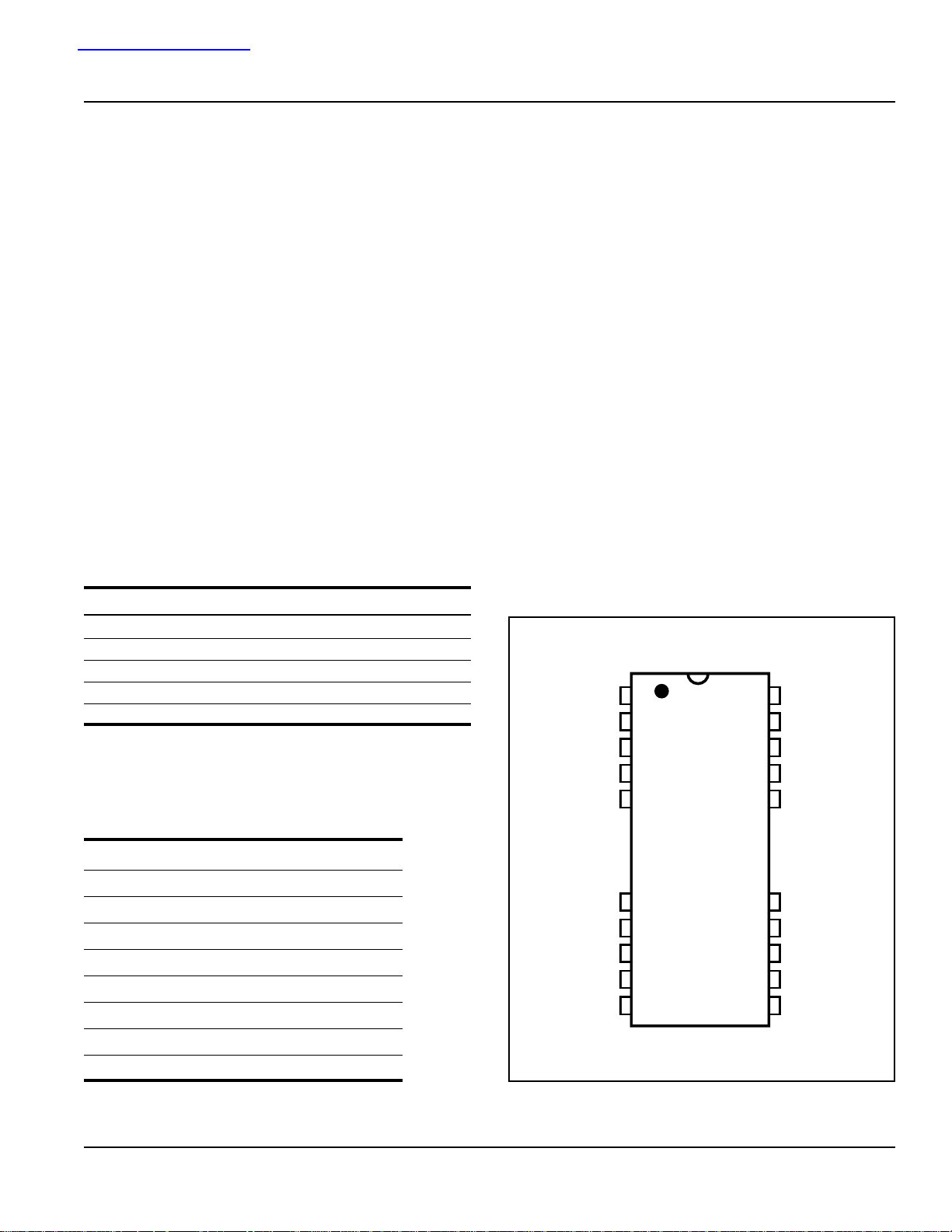
PIN CONFIGURATION
20-Pin SOJ
I/O0
I/O1
WE
RAS
A9
1
2
3
4
5
20
19
18
17
16
GND
I/O3
I/O2
CAS
OE
A0-A9 Address Inputs
I/O0-I/O3 Data Inputs/Outputs
15
14
13
12
11
A8
A7
A6
A5
A4
WE Write Enable
OE Output Enable
RAS Row Address Strobe
CAS Column Address Strobe
VCC Power
GND Ground
NC No Connection
This document contains PRELIMINARY INFORMATION data. ISSI reserves the right to make changes to its products at any time without notice in order to improve design and supply the
best possible product. We assume no responsibility for any errors which may appear in this publication. © Copyright 2001, Integrated Silicon Solution, Inc.
Integrated Silicon Solution, Inc. — 1-800-379-4774
PRELIMINARY INFORMATION Rev. 00A
09/10/01
A0
A1
A2
A3
Vcc
6
7
8
9
10
1
Page 2
IS41C4100
E
IS41LV4100 ISSI
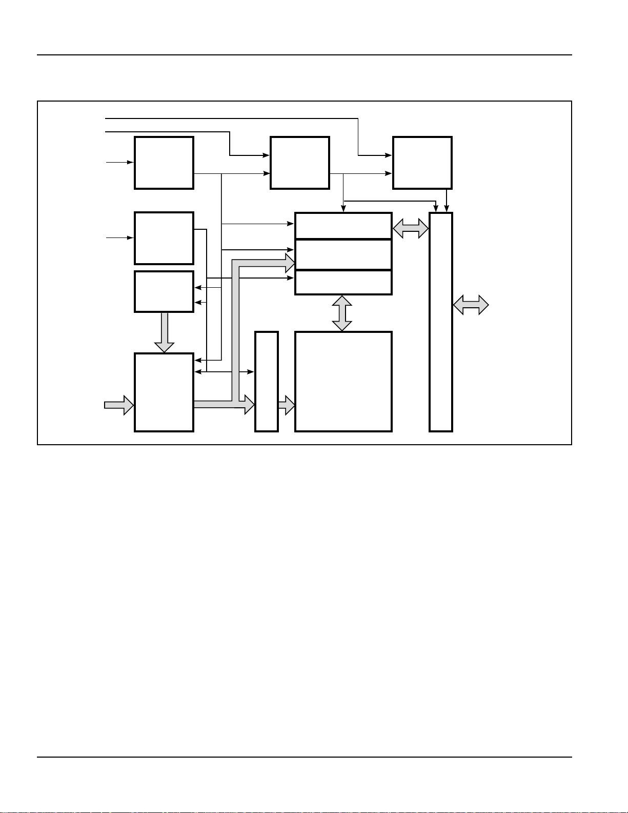
FUNCTIONAL BLOCK DIAGRAM
O
WE
®
CAS
RAS
A0-A9
CAS
CLOCK
GENERATOR
RAS
CLOCK
GENERATOR
REFRESH
COUNTER
ADDRESS
BUFFERS
WE
CAS WE
RAS
CONTROL
LOGICS
COLUMN DECODERS
SENSE AMPLIFIERS
ROW DECODER
OE
CONTROL
LOGIC
OE
DATA I/O BUS
I/O0-I/O3
DATA I/O BUFFERS
MEMORY ARRAY
1,048,576 x 4
2
Integrated Silicon Solution, Inc. — 1-800-379-4774
PRELIMINARY INFORMATION Rev. 00A
09/10/01
Page 3

IS41C4100
IS41LV4100 ISSI
TRUTH TABLE
Function RAS CAS WE OE Address tR/tC I/O
Standby H H X X X High-Z
Read: Word L L H L ROW/COL DOUT
Read: Lower Byte L L H L ROW/COL Lower Byte, DOUT
Upper Byte, High-Z
Read: Upper Byte L H H L ROW/COL Lower Byte, High-Z
Upper Byte, DOUT
Write: Word (Early Write) L L L X ROW/COL DIN
Write: Lower Byte (Early Write) L L L X ROW/COL Lower Byte, DIN
Upper Byte, High-Z
Write: Upper Byte (Early Write) L H L X ROW/COL Lower Byte, High-Z
Upper Byte, DIN
Read-Write
EDO Page-Mode Read
DOUT
EDO Page-Mode Write
(1,2)
LLH→LL→H ROW/COL DOUT, DIN
(2)
1st Cycle: L H→ L H L ROW/COL
2nd Cycle: L H→ L H L NA/COL DOUT
Any Cycle: L L→ H H L NA/NA DOUT
(1)
1st Cycle: L H→ L L X ROW/COL, DIN
2nd Cycle: L H→ L L X NA/COL DIN
®
EDO Page-Mode 1st Cycle: L H→ LH→LL→H ROW/COL
DOUT, DIN
Read-Write
Hidden Refresh
(1,2)
2nd Cycle: L H→ LH→ LL→ H NA/COL DOUT, DIN
2)
Read L→H→L L H L ROW/COL
DOUT
Write L→H→L L L X ROW/COL
DOUT
RAS-Only Refresh L H X X ROW/NA High-Z
CBR Refresh
Notes:
1. These WRITE cycles may also be BYTE WRITE cycles (either LCAS or UCAS active).
2. These READ cycles may also be BYTE READ cycles (either LCAS or UCAS active).
3. At least one of the two CAS signals must be active (LCAS or UCAS).
(3)
H→ L L X X X High-Z
Integrated Silicon Solution, Inc. — 1-800-379-4774
PRELIMINARY INFORMATION Rev. 00A
09/10/01
3
Page 4

IS41C4100
IS41LV4100 ISSI
®
Functional Description
The IS41C4100 and IS41LV4100 is a CMOS DRAM
optimized for high-speed bandwidth, low power applications. During READ or WRITE cycles, each bit is uniquely
addressed through the 19 address bits. The first ten
address bits (A0-A9) are entered as row address and
latter nine bits nine address bits (A0-A8) are entered as
column address. The row address is latched by the Row
Address Strobe (RAS). The column address is latched by
the Column Address Strobe (CAS). RAS is used to latch
the first nine bits and CAS is used the latter nine bits.
Memory Cycle
A memory cycle is initiated by bring RAS LOW and it is
terminated by returning both RAS and CAS HIGH. To
ensures proper device operation and data integrity any
memory cycle, once initiated, must not be ended or
aborted before the minimum tRAS time has expired. A new
cycle must not be initiated until the minimum precharge
time tRP, tCP has elapsed.
Read Cycle
A read cycle is initiated by the falling edge of CAS or OE,
whichever occurs last, while holding WE HIGH. The
column address must be held for a minimum time specified by tAR. Data Out becomes valid only when tRAC, tAA,
tCAC and tOEA are all satisfied. As a result, the access time
is dependent on the timing relationships between these
parameters.
2. Using a CAS-before-RAS refresh cycle. CAS-before-
RAS refresh is activated by the falling edge of RAS,
while holding CAS LOW. In CAS-before-RAS refresh
cycle, an internal 10-bit counter provides the row
addresses and the external address inputs are ignored.
CAS-before-RAS is a refresh-only mode and no data
access or device selection is allowed. Thus, the output
remains in the High-Z state during the cycle.
Extended Data Out Page Mode
EDO page mode operation permits all 512 columns within
a selected row to be randomly accessed at a high data
rate.
In EDO page mode read cycle, the data-out is held to the
next CAS cycle’s falling edge, instead of the rising edge.
For this reason, the valid data output time in EDO page
mode is extended compared with the fast page mode. In
the fast page mode, the valid data output time becomes
shorter as the CAS cycle time becomes shorter. Therefore, in EDO page mode, the timing margin in read cycle
is larger than that of the fast page mode even if the CAS
cycle time becomes shorter.
In EDO page mode, due to the extended data function, the
CAS cycle time can be shorter than in the fast page mode
if the timing margin is the same.
The EDO page mode allows both read and write operations during one RAS cycle, but the performance is
equivalent to that of the fast page mode in that case.
Write Cycle
A write cycle is initiated by the falling edge of CAS and
WE, whichever occurs last. The input data must be valid
at or before the falling edge of CAS or WE, whichever
occurs last.
Refresh Cycle
To retain data, 1024 refresh cycles are required in each
16 ms period. There are two ways to refresh the memory.
1. By clocking each of the 1024 row addresses (A0
through A9) with RAS at least once every 16 ms. Any
read, write, read-modify-write or RAS-only cycle refreshes the addressed row.
4
Power-On
After application of the VCC supply, an initial pause of
200 µs is required followed by a minimum of eight initialization cycles (any combination of cycles containing a
RAS signal).
During power-on, it is recommended that RAS track with
VCC or be held at a valid VIH to avoid current surges.
Integrated Silicon Solution, Inc. — 1-800-379-4774
PRELIMINARY INFORMATION Rev. 00A
09/10/01
Page 5

IS41C4100
IS41LV4100 ISSI
®
ABSOLUTE MAXIMUM RATINGS
(1)
Symbol Parameters Rating Unit
VT Voltage on Any Pin Relative to GND 5V –1.0 to +7.0 V
3.3V -0.5 to 4.6 V
CC Supply Voltage 5V –1.0 to +7.0 V
V
3.3V -0.5 to 4.6 V
IOUT Output Current 50 mA
PD Power Dissipation 1 W
A Commercial Operation Temperature 0 to +70 °C
T
Industrail Temperature –40 to +85 °C
TSTG Storage Temperature –55 to +125 °C
Note:
1. Stress greater than those listed under ABSOLUTE MAXIMUM RATINGS may cause permanent
damage to the device. This is a stress rating only and functional operation of the device at these
or any other conditions above those indicated in the operational sections of this specification is not
implied. Exposure to absolute maximum rating conditions for extended periods may affect
reliability.
RECOMMENDED OPERATING CONDITIONS (Voltages are referenced to GND.)
Symbol Parameter Min. Typ. Max. Unit
VCC Supply Voltage 5V 4.5 5.0 5.5 V
3.3V 3.0 3.3 3.6
VIH Input High Voltage 5V 2.4 — VCC + 1.0 V
3.3V 2.0 — VCC + 0.3
VIL Input Low Voltage 5V –1.0 — 0.8 V
3.3V –0.3 — 0.8
TA Commercial Ambient Temperature 0 — 70 °C
Industrail Ambient Temperature –40 — 85 °C
CAPACITANCE
(1,2)
Symbol Parameter Max. Unit
CIN1 Input Capacitance: A0-A9 5 pF
CIN2 Input Capacitance: RAS, CAS, WE, OE 7pF
CIO Data Input/Output Capacitance: I/O0-I/O3 7 pF
Notes:
1. Tested initially and after any design or process changes that may affect these parameters.
2. Test conditions: T
A = 25°C, f = 1 MHz,
Integrated Silicon Solution, Inc. — 1-800-379-4774
PRELIMINARY INFORMATION Rev. 00A
09/10/01
5
Page 6

IS41C4100
IS41LV4100 ISSI
®
ELECTRICAL CHARACTERISTICS
(1)
(Recommended Operation Conditions unless otherwise noted.)
Symbol Parameter Test Condition Speed Min. Max. Unit
IL Input Leakage Current Any input 0V ≤ VIN ≤ Vcc –55µA
I
Other inputs not under test = 0V
I
IO Output Leakage Current Output is disabled (Hi-Z) –55µA
0V ≤ VOUT ≤ Vcc
VOH Output High Voltage Level IOH = –2.5 mA 2.4 — V
VOL Output Low Voltage Level IOL = +2.1 mA — 0.4 V
I
CC1 Stand-by Current: TTL RAS, CAS ≥ VIH Commercial 5V — 2mA
Industrial 5V — 3
Commercial 3V — 1
Industrial 3V — 4
ICC2 Stand-by Current: CMOS RAS, CAS ≥ VCC – 0.2V 5V — 1mA
3V — 0.5
ICC3 Operating Current: RAS, CAS, -35 — 100 mA
Random Read/Write
Average Power Supply Current
ICC4 Operating Current: RAS = VIL, CAS, -35 — 120 mA
EDO Page Mode
Average Power Supply Current
(2,3,4)
(2,3,4)
Address Cycling, tRC = tRC (min.) -60 — 75
Cycling tPC = tPC (min.) -60 — 65
ICC5 Refresh Current: RAS Cycling, CAS ≥ VIH -35 — 100 mA
RAS-Only
(2,3)
tRC = tRC (min.) -60 — 75
Average Power Supply Current
ICC6 Refresh Current: RAS, CAS Cycling -35 — 100 mA
(2,3,5)
CBR
tRC = tRC (min.) -60 — 75
Average Power Supply Current
Notes:
1. An initial pause of 200 µs is required after power-up followed by eight RAS refresh cycles (RAS-Only or CBR) before proper device
operation is assured. The eight RAS cycles wake-up should be repeated any time the t
2. Dependent on cycle rates.
3. Specified values are obtained with minimum cycle time and the output open.
4. Column-address is changed once each EDO page cycle.
5. Enables on-chip refresh and address counters.
REF refresh requirement is exceeded.
6
Integrated Silicon Solution, Inc. — 1-800-379-4774
PRELIMINARY INFORMATION Rev. 00A
09/10/01
Page 7

IS41C4100
IS41LV4100 ISSI
®
AC CHARACTERISTICS
(1,2,3,4,5,6)
(Recommended Operating Conditions unless otherwise noted.)
-35 -60
Symbol Parameter Min. Max. Min. Max. Units
tRC Random READ or WRITE Cycle Time 60 — 110 — ns
(26)
(9, 25)
(6, 7)
(6, 8, 15)
(10, 20)
(20)
(20)
35 — 60 — ns
— 10 — 15 ns
(6)
— 18 — 30 ns
6 10K 10 10K ns
5 — 10 — ns
35 — 60 — ns
11 28 20 45 ns
0 — 0 — ns
6 — 10 — ns
tRAC Access Time from RAS
tCAC Access Time from CAS
tAA Access Time from Column-Address
tRAS RAS Pulse Width 35 10K 60 10K ns
tRP RAS Precharge Time 20 — 40 — ns
tCAS CAS Pulse Width
tCP CAS Precharge Time
tCSH CAS Hold Time
(21)
tRCD RAS to CAS Delay Time
tASR Row-Address Setup Time 0 — 0 — ns
tRAH Row-Address Hold Time 6 — 10 — ns
tASC Column-Address Setup Time
tCAH Column-Address Hold Time
tAR Column-Address Hold Time 30 — 40 — ns
(referenced to RAS)
tRAD RAS to Column-Address Delay Time
(11)
10 20 15 30 ns
tRAL Column-Address to RAS Lead Time 18 — 30 — ns
tRPC RAS to CAS Precharge Time 0 — 0 — ns
tRSH RAS Hold Time
tCLZ CAS to Output in Low-Z
tCRP CAS to RAS Precharge Time
tOD Output Disable Time
tOE / tOEA Output Enable Time
(27)
(15, 29)
(19, 28, 29)
(15, 16)
(21)
8 — 115 — ns
3 — 3 — ns
5 — 5 — ns
312 312 ns
010 — 15 ns
tOEHC OE HIGH Hold Time from CAS HIGH 10 — 10 — ns
tOEP OE HIGH Pulse Width 10 — 10 — ns
tOES OE LOW to CAS HIGH Setup Time 5 — 5 — ns
tRCS Read Command Setup Time
(17, 20)
0 — 0 — ns
tRRH Read Command Hold Time 0 — 0 — ns
(referenced to RAS)
(12)
tRCH Read Command Hold Time 0 — 0 — ns
(referenced to CAS)
tWCH Write Command Hold Time
(12, 17, 21)
(17, 27)
5 — 10 — ns
tWCR Write Command Hold Time 30 — 50 — ns
(referenced to RAS)
(17)
Integrated Silicon Solution, Inc. — 1-800-379-4774
PRELIMINARY INFORMATION Rev. 00A
09/10/01
7
Page 8

IS41C4100
IS41LV4100 ISSI
®
AC CHARACTERISTICS (Continued)
(1,2,3,4,5,6)
(Recommended Operating Conditions unless otherwise noted.)
-35 -60
Symbol Parameter Min. Max. Min. Max. Units
(14, 20)
(17)
(14, 17, 20)
(18)
(14)
(17)
(17, 21)
(14)
5 — 10 — ns
8 — 15 — ns
8 — 15 — ns
0 — 0 — ns
0 — 0 — ns
6 — 10 — ns
25 — 36 — ns
30 — 49 — ns
tWP Write Command Pulse Width
tWPZ WE Pulse Widths to Disable Outputs 10 — 10 — ns
tRWL Write Command to RAS Lead Time
tCWL Write Command to CAS Lead Time
tWCS Write Command Setup Time
DHR Data-in Hold Time (referenced to RAS)30 — 40 — ns
t
Precharge during WRITE Cycle
t
OEH OE Hold Time from WE during 8 — 15 — ns
READ-MODIFY-WRITE cycle
tDS Data-In Setup Time
tDH Data-In Hold Time
(15, 22)
(15, 22)
tRWC READ-MODIFY-WRITE Cycle Time 80 — 140 — ns
tRWD RAS to WE Delay Time during 45 — 80 — ns
READ-MODIFY-WRITE Cycle
tCWD CAS to WE Delay Time
tAWD Column-Address to WE Delay Time
tPC EDO Page Mode READ or WRITE 12 — 25 — ns
Cycle Time
(24)
tRASP RAS Pulse Width in EDO Page Mode 35 100K 60 100K ns
tCPA Access Time from CAS Precharge
(15)
— 21 — 34 ns
tPRWC EDO Page Mode READ-WRITE 40 — 56 — ns
Cycle Time
(24)
tCOH/tDOH Data Output Hold after CAS LOW 5 — 5 — ns
tOFF Output Buffer Turn-Off Delay from 3 15 3 15 ns
CAS or RAS
(13,15,19, 29)
tWHZ Output Disable Delay from WE 315 315 ns
tCLCH Last CAS going LOW to First CAS 10 — 10 — ns
returning HIGH
tCSR CAS Setup Time (CBR REFRESH)
tCHR CAS Hold Time (CBR REFRESH)
(23)
(30, 20)
(30, 21)
8 — 10 — ns
8 — 10 — ns
tORD OE Setup Time prior to RAS during 0 — 0 — ns
HIDDEN REFRESH Cycle
tREF Refresh Period (1024 Cycles) — 16 — 16 ms
tT Transition Time (Rise or Fall)
(2, 3)
150 150 ns
8
Integrated Silicon Solution, Inc. — 1-800-379-4774
PRELIMINARY INFORMATION Rev. 00A
09/10/01
Page 9

IS41C4100
IS41LV4100 ISSI
Notes:
1. An initial pause of 200 µs is required after power-up followed by eight RAS refresh cycle (RAS-Only or CBR) before proper device
operation is assured. The eight RAS cycles wake-up should be repeated any time the t
IH (MIN) and VIL (MAX) are reference levels for measuring timing of input signals. Transition times, are measured between VIH
2. V
and VIL (or between VIL and VIH) and assume to be 1 ns for all inputs.
3. In addition to meeting the transition rate specification, all input signals must transit between V
a monotonic manner.
4. If CAS and RAS = V
5. If CAS = V
IL, data output may contain data from the last valid READ cycle.
IH, data output is High-Z.
6. Measured with a load equivalent to one TTL gate and 50 pF.
7. Assumes that t
the amount that t
8. Assumes that t
RCD - tRCD (MAX). If tRCD is greater than the maximum recommended value shown in this table, tRAC will increase by
RCD exceeds the value shown.
RCD • tRCD (MAX).
9. If CAS is LOW at the falling edge of RAS, data out will be maintained from the previous cycle. To initiate a new cycle and clear the
data output buffer, CAS and RAS must be pulsed for t
10. Operation with the t
RCD (MAX) limit ensures that tRAC (MAX) can be met. tRCD (MAX) is specified as a reference point only; if tRCD
CP.
is greater than the specified tRCD (MAX) limit, access time is controlled exclusively by tCAC.
11. Operation within the t
RAD (MAX) limit ensures that tRCD (MAX) can be met. tRAD (MAX) is specified as a reference point only; if tRAD
is greater than the specified tRAD (MAX) limit, access time is controlled exclusively by tAA.
12. Either t
13. t
RCH or tRRH must be satisfied for a READ cycle.
OFF (MAX) defines the time at which the output achieves the open circuit condition; it is not a reference to VOH or VOL.
14. tWCS, tRWD, tAWD and tCWD are restrictive operating parameters in LATE WRITE and READ-MODIFY-WRITE cycle only. If tWCS •
WCS (MIN), the cycle is an EARLY WRITE cycle and the data output will remain open circuit throughout the entire cycle. If tRWD •
t
RWD (MIN), tAWD • tAWD (MIN) and tCWD • tCWD (MIN), the cycle is a READ-WRITE cycle and the data output will contain data read
t
from the selected cell. If neither of the above conditions is met, the state of I/O (at access time and until CAS and RAS or OE go
back to V
IH) is indeterminate. OE held HIGH and WE taken LOW after CAS goes LOW result in a LATE WRITE (OE-controlled)
cycle.
15. Output parameter (I/O) is referenced to corresponding CAS input, I/O0-I/O7 by LCAS and I/O8-I/O15 by UCAS.
16. During a READ cycle, if OE is LOW then taken HIGH before CAS goes HIGH, I/O goes open. If OE is tied permanently LOW, a
LATE WRITE or READ-MODIFY-WRITE is not possible.
17. Write command is defined as WE going low.
18. LATE WRITE and READ-MODIFY-WRITE cycles must have both t
OD and tOEH met (OE HIGH during WRITE cycle) in order to
ensure that the output buffers will be open during the WRITE cycle. The I/Os will provide the previously written data if CAS
remains LOW and OE is taken back to LOW after t
19. The I/Os are in open during READ cycles once t
OEH is met.
OD or tOFF occur.
20. The first χCAS edge to transition LOW.
21. The last χCAS edge to transition HIGH.
22. These parameters are referenced to CAS leading edge in EARLY WRITE cycles and WE leading edge in LATE WRITE or
READ-MODIFY-WRITE cycles.
23. Last falling χCAS edge to first rising χCAS edge.
24. Last rising χCAS edge to next cycle’s last rising χCAS edge.
25. Last rising χCAS edge to first falling χCAS edge.
26. Each χCAS must meet minimum pulse width.
27. Last χCAS to go LOW.
28. I/Os controlled, regardless UCAS and LCAS.
29. The 3 ns minimum is a parameter guaranteed by design.
30. Enables on-chip refresh and address counters.
REF refresh requirement is exceeded.
IH and VIL (or between VIL and VIH) in
®
Integrated Silicon Solution, Inc. — 1-800-379-4774
PRELIMINARY INFORMATION Rev. 00A
09/10/01
9
Page 10
IS41C4100
Don't Care
IS41LV4100 ISSI
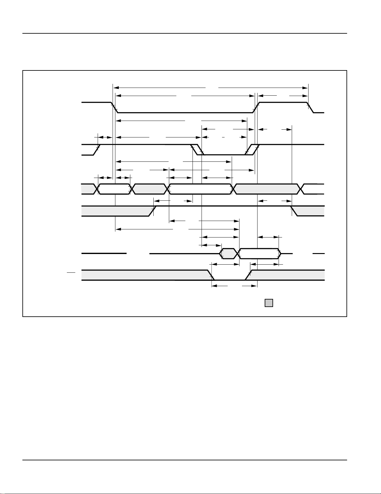
AC WAVEFORMS
READ CYCLE
t
RC
t
RAS
CAS
t
CRP
t
ASR
t
RAH
t
RAD
t
RCD
t
ASC
t
AR
RAS
t
CSH
t
CAS
t
RAL
t
RSH
t
CLCH
t
CAH
t
RRH
t
RP
®
ADDRESS
Row Column Row
t
RCS
WE
t
AA
t
RAC
t
CAC
t
CLC
I/O
Open Open
t
OE
OE
Note:
1. tOFF is referenced from rising edge of RAS or CAS, whichever occurs last.
t
OES
Valid Data
t
RCH
t
OFF
t
(1)
OD
10
Integrated Silicon Solution, Inc. — 1-800-379-4774
PRELIMINARY INFORMATION Rev. 00A
09/10/01
Page 11
IS41C4100
IS41LV4100 ISSI
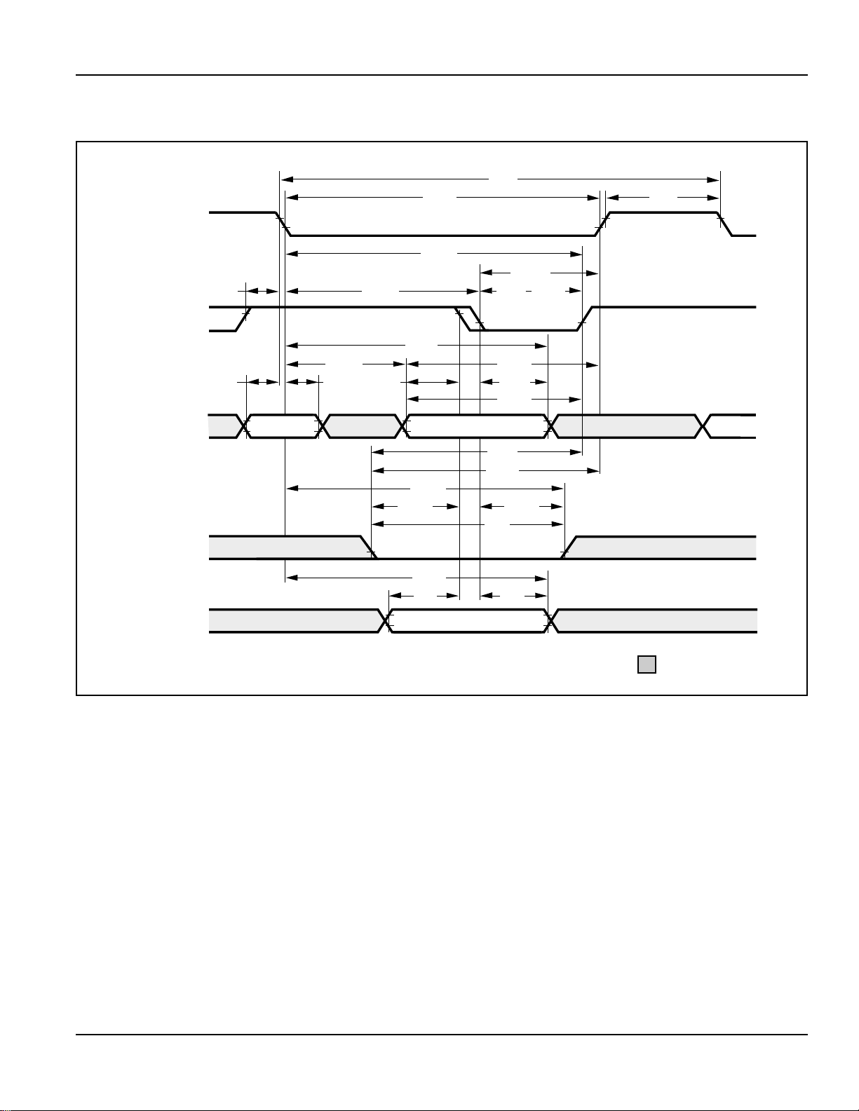
EARLY WRITE CYCLE (OE = DON'T CARE)
t
RC
t
RAS
CAS
t
CRP
t
ASR
t
t
RAH
RAD
t
RCD
t
ASC
RAS
t
CSH
t
RSH
t
CAS
t
CLCH
t
AR
t
RAL
t
CAH
t
ACH
t
RP
®
ADDRESS
WE
I/O
Row Column Row
t
CWL
t
RWL
t
WCR
t
t
WP
t
DH
WCH
t
WCS
t
DHR
t
DS
Valid Data
Don't Care
Integrated Silicon Solution, Inc. — 1-800-379-4774
PRELIMINARY INFORMATION Rev. 00A
09/10/01
11
Page 12
IS41C4100
IS41LV4100 ISSI
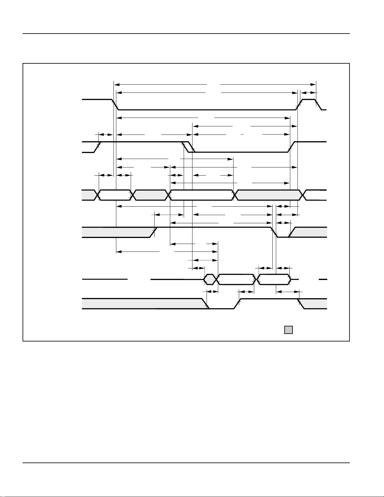
READ WRITE CYCLE (LATE WRITE and READ-MODIFY-WRITE Cycles)
t
RWC
t
RAS
CAS
t
CRP
t
ASR
t
RAH
t
RAD
t
RCD
t
ASC
t
AR
t
CSH
RAS
t
CAH
t
CAS
t
RSH
t
t
t
RAL
ACH
CLCH
t
RP
®
ADDRESS
WE
I/O
OE
Row Column Row
t
RWD
t
t
RCS
t
AA
t
RAC
t
CAC
t
CLZ
Open Open
t
OE
CWD
t
AWD
Valid D
t
OD
t
OUT
DS
Valid D
t
CWL
t
RWL
t
WP
t
DH
IN
t
OEH
Don't Care
12
Integrated Silicon Solution, Inc. — 1-800-379-4774
PRELIMINARY INFORMATION Rev. 00A
09/10/01
Page 13
IS41C4100
n
IS41LV4100 ISSI
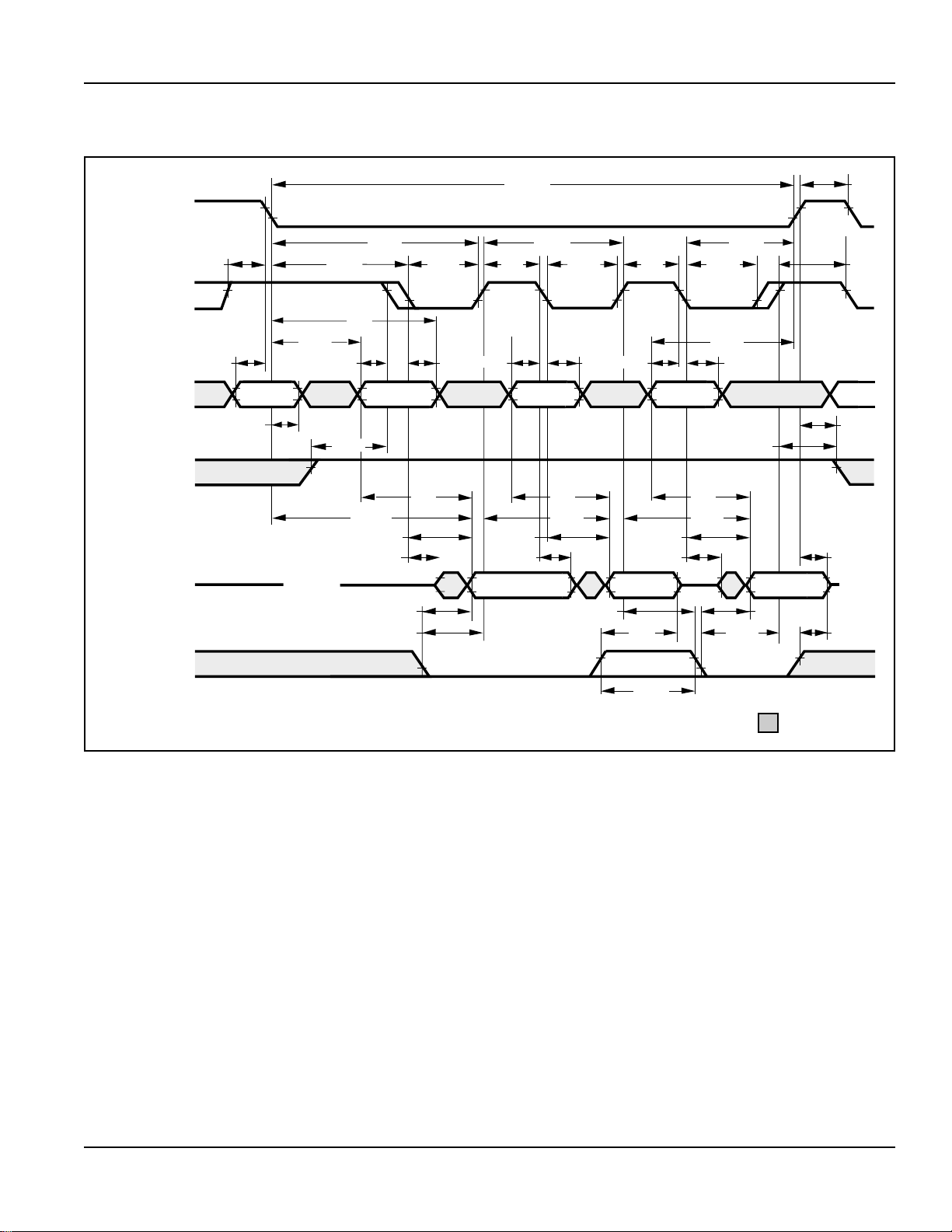
EDO-PAGE-MODE READ CYCLE
t
RASP
RAS
t
RP
®
CAS
ADDRESS
WE
I/O
OE
t
CRP
t
ASR
t
CSH
t
t
t
AA
CAS,
CLCH
t
CAH
t
RCD
t
AR
t
RAD
t
ASC
Row Row
t
RAH
Column Column
t
RCS
t
RAC
t
CAC
t
CLZ
Open Ope
t
OE
t
OES
t
CP
t
ASC
t
CAC
t
COH
Valid Data
(1)
t
PC
Column
t
AA
t
CPA
t
CAS,
t
CLCH
t
t
OEHC
CAH
t
CP
t
ASC
t
CAC
t
CLZ
Valid Data
t
OD
t
OEP
t
AA
t
CPA
t
CAS,
t
CLCH
t
RAL
t
t
CAH
t
OES
RSH
t
RCH
Valid Data
t
OE
t
t
OFF
t
OD
t
CP
RRH
Don't Care
Note:
PC can be measured from falling edge of CAS to falling edge of CAS, or from rising edge of CAS to rising edge of CAS. Both
1. t
measurements must meet the tPC specifications.
Integrated Silicon Solution, Inc. — 1-800-379-4774
PRELIMINARY INFORMATION Rev. 00A
09/10/01
13
Page 14
IS41C4100
IS41LV4100 ISSI
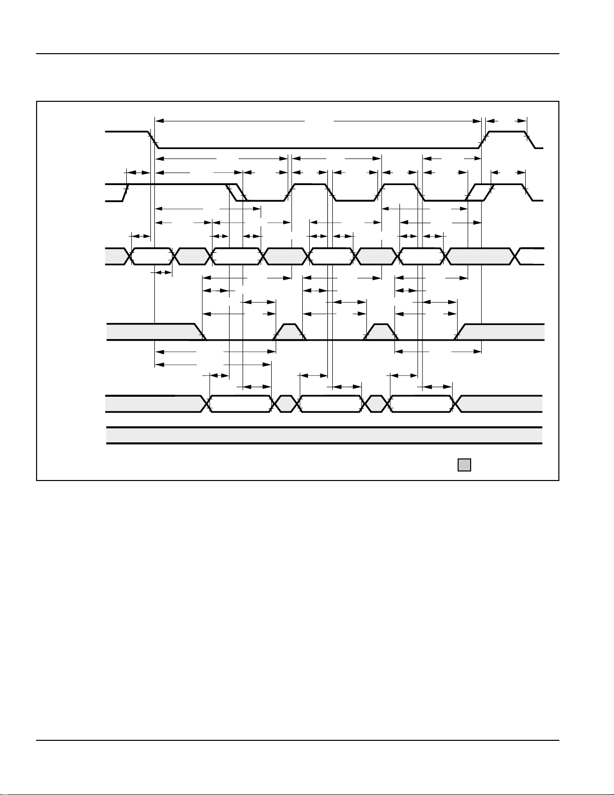
EDO-PAGE-MODE EARLY-WRITE CYCLE
t
RAS
CAS
t
CRP
t
ASR
t
RAD
t
RCD
t
ASC
t
AR
t
CSH
t
ACH
t
CAS,
t
CLCH
t
CAH
t
ASC
t
CP
RASP
t
PC
t
CAS,
t
CLCH
t
ACH
t
CAH
t
ASC
t
CP
t
CAS,
t
CLCH
t
ACH
t
RAL
t
RSH
t
CAH
t
t
RP
CP
®
ADDRESS
WE
I/O
OE
Row Row
t
RAH
t
Column Column
t
CWL
t
WCS
t
WCH
t
WP
t
WCR
t
DHR
DS
t
DH
t
Valid Data
DS
Column
t
CWL
t
WCS
t
WCH
t
WP
t
DH
Valid Data
t
DS
t
WCH
t
DH
Valid Data
t
CWL
t
WCS
t
WP
t
RWL
Don't Care
14
Integrated Silicon Solution, Inc. — 1-800-379-4774
PRELIMINARY INFORMATION Rev. 00A
09/10/01
Page 15
IS41C4100
IS41LV4100 ISSI
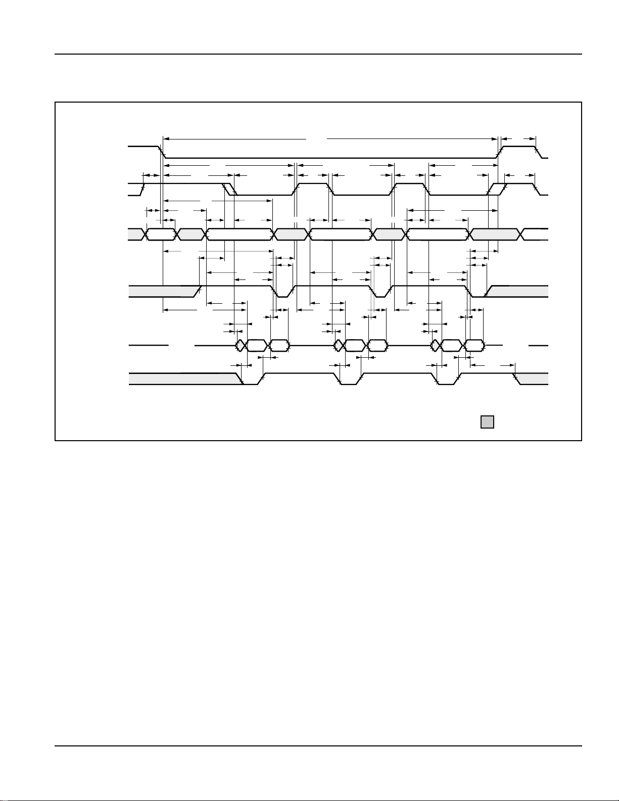
EDO-PAGE-MODE READ-WRITE CYCLE (LATE WRITE and READ-MODIFY WRITE Cycles)
t
RAS
CAS
ADDRESS
WE
I/O
OE
RASP
/ t
t
PRWC
AWD
t
t
t
CWD
D
(1)
CAS, tCLCH
CAH
t
CWL
t
WP
t
DH
t
DS
OUT
t
RSH
t
t
OE
CAS, tCLCH
t
RAL
t
CAH
t
RWL
t
CWL
t
WP
t
AWD
t
CWD
AA
t
DH
t
DS
D
OUT
t
IN
OD
D
t
CP
t
ASC
t
CPA
t
CAC
t
CLZ
D
IN
t
OD
t
t
t
t
RWD
t
RCS
t
t
ASC
RCD
CSH
t
AR
t
CAS, tCLCH
t
CAH
t
ASC
Column Column
t
CWL
t
WP
t
AWD
t
CWD
t
t
RAC
t
CAC
t
CLZ
t
OE
AA
t
DH
t
DS
D
OUT
t
IN
OD
D
t
CRP
t
ASR
t
RAH
t
RAD
Row Row
Open Open
t
t
CAC
t
CLZ
CP
t
CPA
t
OE
PC
Column
t
AA
t
OEH
t
RP
t
CP
®
Don't Care
Note:
PC can be measured from falling edge of CAS to falling edge of CAS, or from rising edge of CAS to rising edge of CAS. Both
1. t
measurements must meet the tPC specifications.
Integrated Silicon Solution, Inc. — 1-800-379-4774
PRELIMINARY INFORMATION Rev. 00A
09/10/01
15
Page 16
IS41C4100
IS41LV4100 ISSI
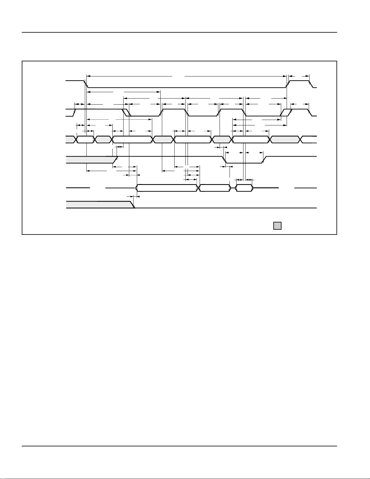
EDO-PAGE-MODE READ-EARLY-WRITE CYCLE (Psuedo READ-MODIFY WRITE)
®
RAS
CAS
ADDRESS
WE
I/O
OE
tRASP
tCSH
tCRP
tASR
tRAH
Row Row
tRCD
tAR
tRAD
Column (A) Column (N)
tRCS
tAA
tRAC
tCAC
Open Open
tOE
tPC
tCP
tASCtASC
Valid Data (A)
Column (B)
tCPA
tCAC
tCOH
tAA
tPC
tCAS tCAS
tCAHtCAH
tRCH
tWHZ
Valid Data (B)
tASC
tDS
tWCS
tRSH
tCAS
tACH
tRAL
tCAH
tWCH
tDH
D
IN
tRP
tCPtCP
Don't Care
16
Integrated Silicon Solution, Inc. — 1-800-379-4774
PRELIMINARY INFORMATION Rev. 00A
09/10/01
Page 17
IS41C4100
IS41LV4100 ISSI
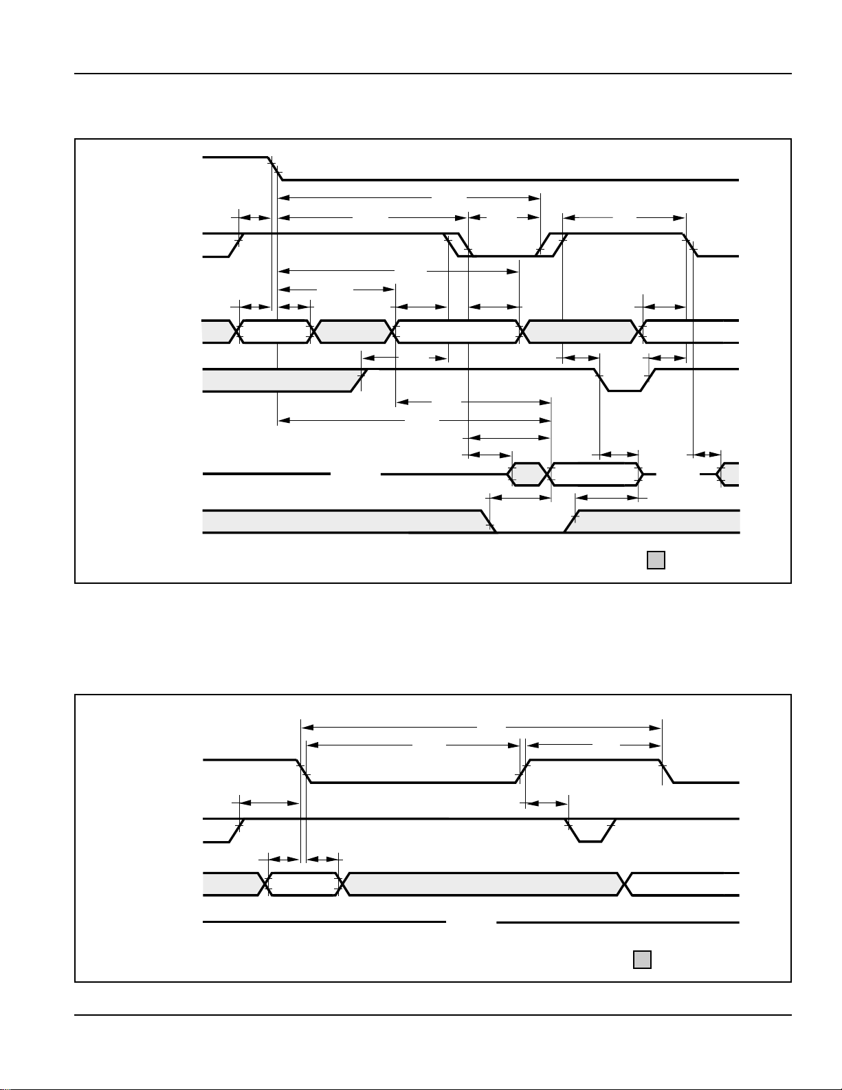
READ CYCLE (With WE-Controlled Disable)
RAS
t
CSH
t
CAS
CRP
t
ASR
t
t
RAD
RAH
t
RCD
t
ASC
t
AR
t
CAS
t
CAH
t
ASC
t
CP
®
ADDRESS
Row Column
t
RCS
WE
t
AA
t
RAC
t
CAC
t
CLZ
I/O
Open Open
t
OE
OE
RAS-ONLY REFRESH CYCLE (OE, WE = DON'T CARE)
t
t
RAS
RC
t
RCH
t
WHZ
Valid Data
t
RP
t
RCS
Column
t
CLZ
t
OD
Don't Care
RAS
t
CRP
CAS
t
RAH
ADDRESS
t
ASR
Row Row
I/O
Integrated Silicon Solution, Inc. — 1-800-379-4774
PRELIMINARY INFORMATION Rev. 00A
09/10/01
Open
t
RPC
Don't Care
17
Page 18
IS41C4100
C
R
IS41LV4100 ISSI
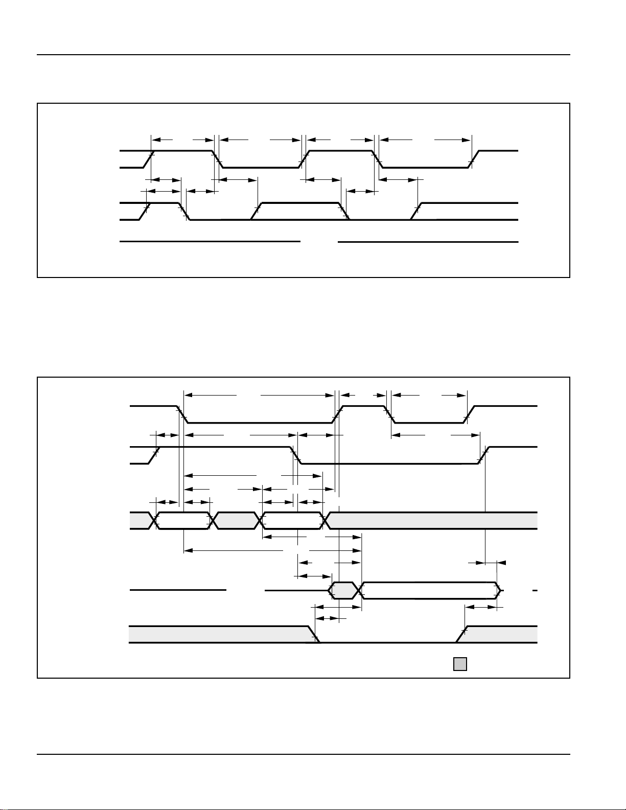
CBR REFRESH CYCLE (Addresses; WE, OE = DON'T CARE)
t
AS
AS
t
RPC
t
CP
t
RP
t
CHR
t
CSR
RAS
t
RPC
t
RP
t
CSR
t
RAS
t
CHR
®
I/O
Open
HIDDEN REFRESH CYCLE (WE = HIGH; OE = LOW)
t
RAS
RAS
t
CAS
ADDRESS
I/O
CRP
t
ASR
Row Column
t
RCD
t
AR
t
RAD
t
RAH
t
ASC
t
CLZ
t
RAL
t
RAC
t
AA
t
CAC
Open Open
t
OE
t
CAH
(1)
t
RSH
t
t
RP
ORD
t
RAS
t
CHR
Valid Data
t
OFF
(2)
t
OD
OE
Don't Care
Notes:
1. A Hidden Refresh may also be performed after a Write Cycle. In this case, WE = LOW and OE = HIGH.
OFF is referenced from rising edge of RAS or CAS, whichever occurs last.
2. t
18
Integrated Silicon Solution, Inc. — 1-800-379-4774
PRELIMINARY INFORMATION Rev. 00A
09/10/01
Page 19

IS41C4100
IS41LV4100 ISSI
®
ORDERING INFORMATION : 5V
Commercial Range: 0
Speed (ns) Order Part No. Package
35 IS41C4100-35J 20-pin, 300-mil SOJ
60 IS41C4100-60J 20-pin, 300-mil SOJ
ORDERING INFORMATION : 5V
Industrail Range: -40
Speed (ns) Order Part No. Package
60 IS41C4100-60JI 20-pin, 300-mil SOJ
⋅⋅
⋅C to 70
⋅⋅
⋅⋅
⋅C to 85
⋅⋅
⋅⋅
⋅C
⋅⋅
⋅⋅
⋅C
⋅⋅
ORDERING INFORMATION : 3.3V
Commercial Range: 0
Speed (ns) Order Part No. Package
35 IS41LV4100-35J 20-pin, 300-mil SOJ
60 IS41LV4100-60J 20-pin, 300-mil SOJ
ORDERING INFORMATION : 3.3V
Industrail Range: -40
Speed (ns) Order Part No. Package
60 IS41LV4100-60JI 20-pin, 300-mil SOJ
⋅⋅
⋅C to 70
⋅⋅
⋅⋅
⋅C to 85
⋅⋅
⋅⋅
⋅C
⋅⋅
⋅⋅
⋅C
⋅⋅
Integrated Silicon Solution, Inc. — 1-800-379-4774
PRELIMINARY INFORMATION Rev. 00A
09/10/01
®
ISSI
Integrated Silicon Solution, Inc.
2231 Lawson Lane
Santa Clara, CA 95054
Tel: 1-800-379-4774
Fax: (408) 588-0806
E-mail: [email protected]
www.issi.com
19
 Loading...