

Datasheet IS27LV020-15T, IS27LV020-15PLI, IS27LV020-12TI, IS27LV020-12T, IS27LV020-12PLI Datasheet (ISSI)
...Page 1
ISS I
®
IS27LV020
Integrated Silicon Solution, Inc.
1
EP019-0A
12/19/97
ISSI reserves the right to make changes to its products at any time without notice in order to improve design and supply the best possible product. We assume no responsibility for any errors which
may appear in this publication. © Copyright 1997, Integrated Silicon Solution, Inc.
FEATURES
• Single 2.7V to 3.6V power supply
• Fast access time: 90 ns
• JEDEC-approved pinout
• Low power consumption
— 20 µA (max) CMOS standby current
— 10 mA (max) active current at 5 MHz
• High-speed programming
— Typically less than 16 seconds
• Industrial and commercial temperature ranges
available
• Standard 32-pin DIP, PLCC and TSOP
packages
DESCRIPTION
The ISSI IS27LV020 is a low voltage, low power, high-speed
1 megabit (256K-word by 8-bit) CMOS Programmable ReadOnly Memory. It utilizes the standard JEDEC pinout making it
funtionally compatible with the IS27C020 EPROM. The
IS27LV020 operates from a 2.7V to 3.6V power supply.
The superior access time combined with low power consumption is the result of innovative design and process technology.
Maximum power consumption in standby mode is 72 µW. If the
device is constantly accessed at 5 MHz, then the maximum
power consumption is increased to 36 mW. These power
ratings are significantly lower than the standard IS27C020
EPROM.
The IS27LV020 uses ISSI's write programming algorithm
which allows the entire chip to be programmed in typically less
than 30 seconds.
This product is available in One-Time Programmble (OTP)
PDIP, PLCC, and TSOP packages over commercial and
industrial temperature ranges.
IS27LV020
262,144 x 8 LOW VOLTAGE CMOS EPROM
ISSI
®
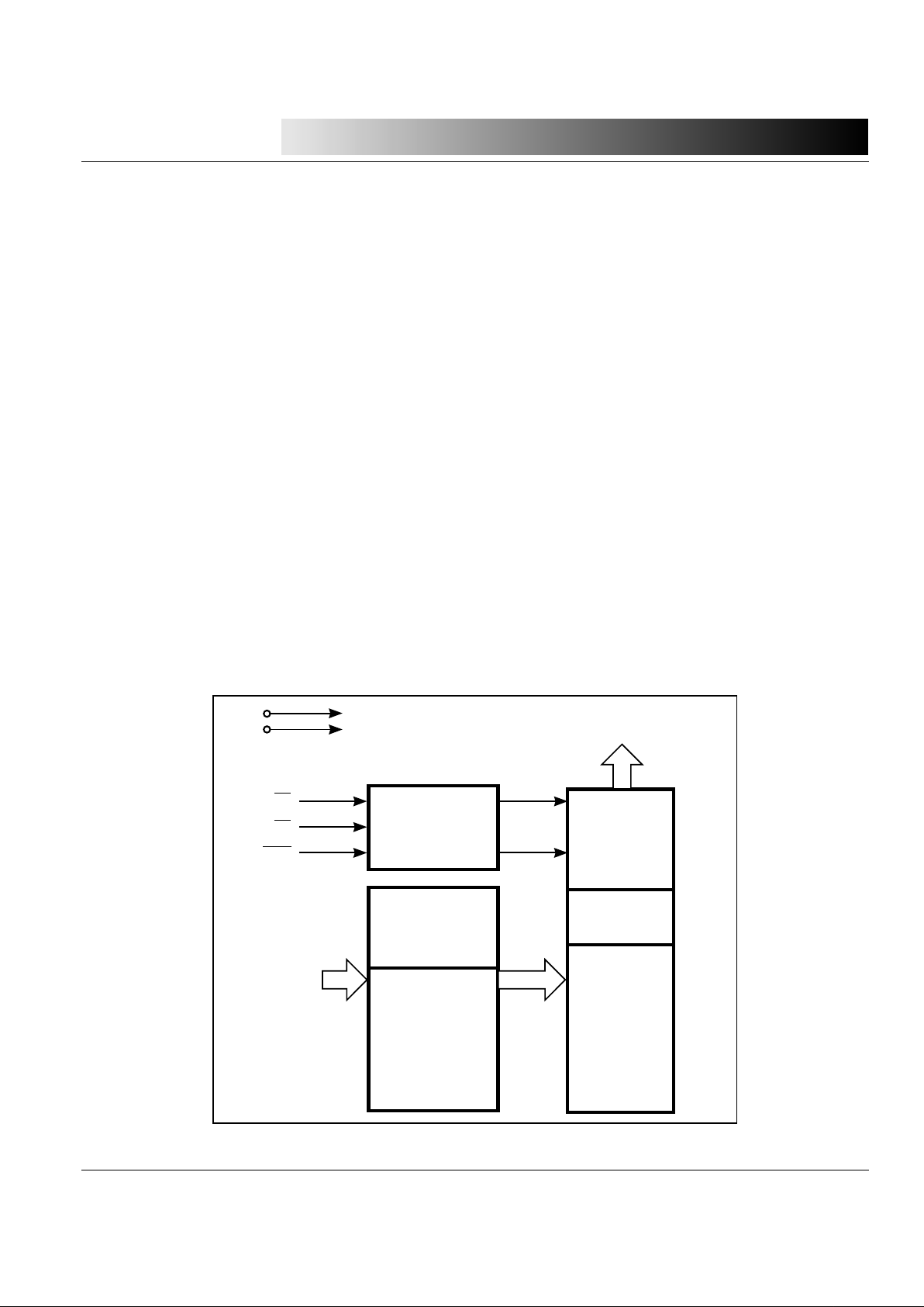
FUNCTIONAL BLOCK DIAGRAM
VCC
GND
OE
OUTPUT ENABLE
CHIP ENABLE
AND
PROG LOGIC
2,097,152-BIT
CELL MATRIX
CE
PGM
OUTPUT
BUFFERS
Y
GATING
X
DECODER
Y
DECODER
18
A0-A17
8
DQ0-DQ7
ADVANCE INFORMATION
DECEMBER 1997
Page 2
ISS I
®
IS27LV020
2
Integrated Silicon Solution, Inc.
EP019-0A
12/19/97
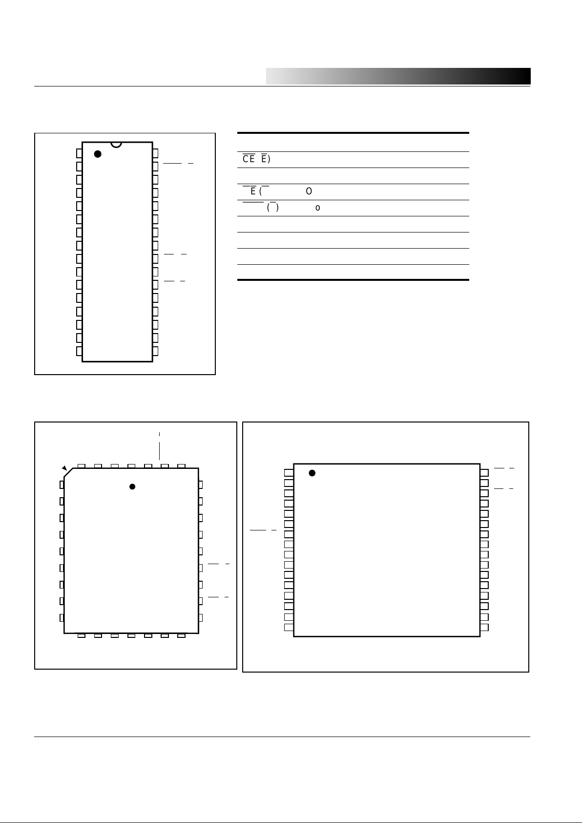
PIN CONFIGURATIONS
32-Pin DIP
PIN DESCRIPTIONS
A0-A17 Address Inputs
CE (E
) Chip Enable Input
DQ0-DQ7 Data Inputs/Outputs
OE (G
) Output Enable Input
PGM (P
) Program Enable Input
Vcc Power Supply Voltage
VPP Program Supply Voltage
GND Ground
NC No Internal Connection
32-Pin PLCC
32-Pin TSOP
1
2
3
4
5
6
7
8
9
10
11
12
13
14
15
16
32
31
30
29
28
27
26
25
24
23
22
21
20
19
18
17
VPP
A16
A15
A12
A7
A6
A5
A4
A3
A2
A1
A0
DQ0
DQ1
DQ2
GND
VCC
PGM (P)
A17
A14
A13
A8
A9
A11
OE (G)
A10
CE (E)
DQ7
DQ6
DQ5
DQ4
DQ3
DQ1
DQ2
GND
DQ3
DQ4
DQ5
DQ6
A12
A15
A16
VPP
VCC
PGM (P)
A17
A14
A13
A8
A9
A11
OE (G)
A10
CE (E)
DQ7
A7
A6
A5
A4
A3
A2
A1
A0
DQ0
5
6
7
8
9
10
11
12
13
29
28
27
26
25
24
23
22
21
INDEX
4 3 2 1 32 31 30
14 15 16 17 18 19 20
1
2
3
4
5
6
7
8
9
10
11
12
13
14
15
16
32
31
30
29
28
27
26
25
24
23
22
21
20
19
18
17
A11
A9
A8
A13
A14
A17
PGM (P)
VCC
VPP
A16
A15
A12
A7
A6
A5
A4
OE (G)
A10
CE (E)
DQ7
DQ6
DQ5
DQ4
DQ3
GND
DQ2
DQ1
DQ0
A0
A1
A2
A3
Page 3

ISS I
®
IS27LV020
Integrated Silicon Solution, Inc.
3
EP019-0A
12/19/97
FUNCTIONAL DESCRIPTION
Programming the IS27LV020
Upon delivery, the IS27LV020 has 2,097,152 bits in the
"ONE", or HIGH state. "ZEROs" are loaded into the
IS27LV020 through the procedure of programming.
The programming mode is entered when 12.5V ± 0.25V is
applied to the VPP pin, VCC = 6V, CE and
PGM
is at VIL, and
OE
is at VIH. For programming, the data to be programmed
is applied eight bits in parallel to the data output pins.
The write programming algorithm reduces programming
time by using 100 µs programming pulses followed by a
byte verification to determine whether the byte has been
successfully programmed. If the data does not verify, an
additional pulse is applied for a maximum of 25 pulses.
This process is repeated while sequencing through each
address of the EPROM.
The write programming algorithm programs and verifies at
VCC = 6V and VPP = 12.5V. After the final address is
completed, all byte are compared to the original data with
VCC = 5.25V.
Program Inhibit
Programming of multiple IS27LV020s in parallel with different data is also easily accomplished. Except for CE, all
like inputs of the parallel IS27LV020 may be common. A
TTL low-level program pulse applied to an IS27LV020
CE
input with VPP = 12.5V ± 0.25V, PGM LOW and OE HIGH
will program that IS27LV020. A high-level CE input inhibits
the other IS27LV020 from being programmed.
Program Verify
A verify should be performed on the programmed bits to
determine that they were correctly programmed. The
verify should be performed with OE and CE at VIL,
PGM
at
VIH, and VPP between 12.25V and 12.75V.
Auto Select Mode
The auto select mode allows the reading out of a binary
code from an EPROM that will identify its manufacturer
and type. This mode is intended for use by programming
equipment for the purpose of automatically matching the
device to be programmed with its corresponding programming algorithm. This mode is functional in the 25°C ± 5°C
ambient temperature range that is required when programming the IS27LV020.
To activate this mode, the programming equipment must
force 12.0V ± 0.5V on address line A9 of the IS27LV020.
Two identifier bytes may then be sequenced from the
device outputs by toggling address line A0 from VIL to VIH.
All other address lines must be held at VIL during auto
select mode.
Byte 0 (A0 = VIL) represents the manufacturer code, and
byte 1 (A0 = VIH), the device identifier code. For the
IS27LV020, these two identifier bytes are given in the
Mode Select table. All identifiers manufacturer and device
codes will possess odd parity, with the MSB (DQ7) defined
as the parity bit.
Read Mode
The IS27LV020 has two control functions, both of which
must be logically satisfied in order to obtain data at the
outputs. Chip Enable (CE) is the power control and should
be used for device selection. Assuming that addresses are
stable, address access time (tACC) is equal to the delay
from CE to output (tCE). Output Enable (OE) is the output
control and should be used to get data to the output pins,
independent of device selection. Data is available at the
outputs tOE after the falling edge of OE assuming that
CE
has been LOW and addresses have been stable for at
least tACC – tOE.
Standby Mode
The IS27LV020 has a standby mode which reduces the
maximum VCC active current. It is placed in standby mode
when CE is at VCC ± 0.3V. The amount of current drawn in
standby mode depends on the frequency and the number
of address pins switching. The IS27LV020 is specified
with 50% of the address lines toggling at 5 MHz. A
reduction of the frequency or quantity of address lines
toggling will significantly reduce the actual standby current.
Page 4
ISS I
®
IS27LV020
4
Integrated Silicon Solution, Inc.
EP019-0A
12/19/97
TRUTH TABLE
(1,2)
Mode
CECE
CECE
CE
OEOE
OEOE
OE
PGMPGM
PGMPGM
PGM
A0 A9 VPP Outputs
Read VIL VIL XXXVCC DOUT
Output Disable VIL VIH XXXVCC Hi-Z
Standby VIH XXXXVCC Hi-Z
Program VIL VIH VIL XXVPP DIN
Program Verify VIL VIL VIH XXVPP DOUT
Program Inhibit VIH XXXXVPP Hi-Z
Auto Select
(3,5)
Manufacturer Code VIL VIL XVIL VH VCC D5H
Device Code VIL VIL XVIH VH VCC 0EH
Notes:
1. VH = 12.0V ± 0.5V.
2. X = Either V
IH or VIL.
3. A1-A8 = A10-A17 = V
IL.
4. See DC Programming Characteristics for VPP voltage during programming.
5. The IS27LV020 can use the same write algorithm during program as other IS27C020 or IS27020 devices.
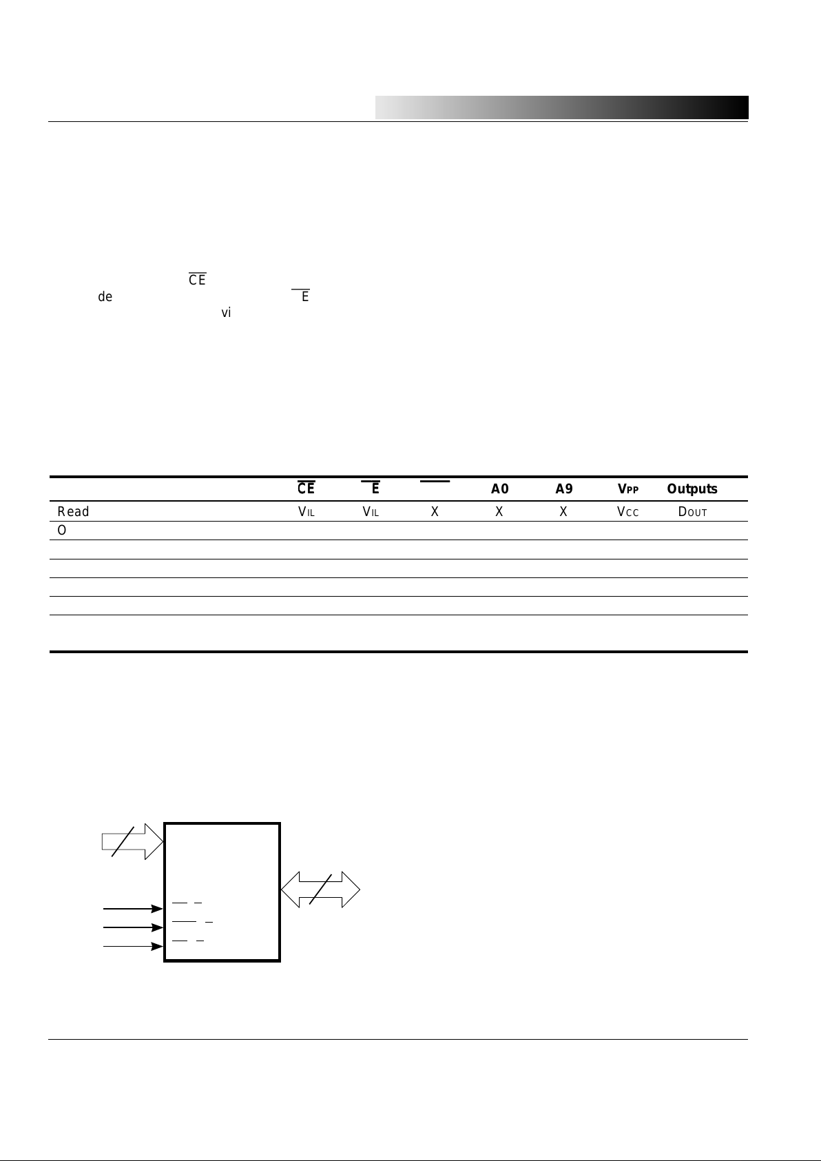
LOGIC SYMBOL
Output OR-Tieing
To accommodate multiple memory connections, a twoline control function is provided to allow for:
1. Low memory power dissipation, and
2. Assurance that output bus contention will not
occur.
It is recommended that CE be decoded and used as the
primary device-selecting function, while OE be made a
common connection to all devices in the array and connected to the READ line from the system control bus. This
assures that all deselected memory devices are in their
low-power standby mode and that the output pins are only
active when data is desired from a particular memory
device.
System Applications
During the switch between active and standby conditions,
transient current peaks are produced on the rising and
falling edges of Chip Enable. The magnitude of these
transient current peaks is dependent on the output capacitance loading of the device at a minimum, a 0.1 µF ceramic
capacitor (high-frequency, low inherent inductance) should
be used on each device between VCC and GND to minimize transient effects. In addition, to overcome the voltage
drop caused by the inductive effects of the printed circuit
board traces on EPROM arrays, a 4.7 µF bulk electrolytic
capacitor should be used between VCC and GND for each
eight devices. The location of the capacitor should be
close to where the power supply is connected to the array.
18
8
DQ0-DQ7
A0-A17
CE (E)
PGM (P)
OE (G)
Page 5

ISS I
®
IS27LV020
Integrated Silicon Solution, Inc.
5
EP019-0A
12/19/97
ABSOLUTE MAXIMUM RATINGS
(1)
Symbol Parameter Value Unit
VTERM Terminal Voltage with Respect to GND
All pins except A9 and VPP –0.6 to VCC + 0.5
(2)
V
VPP VCC – 0.3 to 13.5
(2,3)
V
A9 –0.6 to 13.5
(2,3)
V
VCC –0.6 to 7.0
(2)
V
TA Ambient Temperature with Power Applied –65 to +125 °C
TSTG Storage Temperature (OTP) –65 to +125 °C
TSTG Storage Temperature (All others) –65 to +150 °C
Notes:
1. Stress greater than those listed under ABSOLUTE MAXIMUM RATINGS may cause permanent damage to the
device. This is a stress rating only and functional operation of the device at these or any other conditions above
those indicated in the operational sections of this specification is not implied. Exposure to absolute maximum
rating conditions for extended periods may affect reliability.
2. Minimum DC input voltage is –0.5V. During transitions, inputs may undershoot to –2.0V for periods less than 10
ns. Maximum DC voltage on output pins is Vcc + 0.5V which may overshoot to Vcc + 2.0V for periods less than
10 ns.
3. Maximum DC voltage on A9 or V
PP may overshoot to +13.5V for periods less than 10 ns.
OPERATING RANGE
Range Ambient Temperature VCC
Commercial 0°C to +70°C 2.7 – 3.6V
Industrial
(1)
–40°C to +85°C 2.7 – 3.6V
Note:
1. Operating ranges define those limits between which the
functionally of the device is guaranteed.
DC ELECTRICAL CHARACTERISTICS
(1,2,3)
(Over Operating Range)
Symbol Parameter Test Conditions Min. Max. Unit
VOH Output HIGH Voltage VCC = Min., IOH = –400 µA 2.4 — V
VOL Output LOW Voltage VCC = Min., IOL = 2.0 mA — 0.4 V
VIH Input HIGH Voltage
(4)
2.0 VCC + 0.5 V
VIL Input LOW Voltage
(4)
–0.3 0.8 V
ILI Input Load Current VIN = 0V to +VCC —5µA
ILO Output Leakage Current VOUT = 0V to +VCC —5µA
Notes:
1. VCC must be applied simultaneously or before VPP and removed simultaneously or after VPP. Never try to force VPP LOW to 1V
below V
CC. Manufacturer suggests to tie VPP and VCC together during the READ operation.
2. Caution: the IS27LV020 must not be removed from (or inserted into) a socket when V
CC or VPP is applied.
3. Minimum DC input voltage is –0.5V. During transitions, the inputs may undershoot to –2.0V for periods less than 10 ns.
Maximum DC voltage on output pins is V
CC + 0.5V which may overshoot to VCC + 2.0V for periods less than 10 ns.
4. Tested under static DC conditions.
Page 6

ISS I
®
IS27LV020
6
Integrated Silicon Solution, Inc.
EP019-0A
12/19/97
POWER SUPPLY CHARACTERISTICS
(1,2,5)
(Over Operating Range)
Symbol Parameter Test Conditions Min. Max. Unit
ICC1 Vcc Operating VCC = Max., CE = VIL —10mA
Supply Current
(3)
IOUT = 0 mA, f = 5 MHz
(Open outputs)
IPP1 VPP Current During VCC = Max., CE = OE = VIL —10µA
Read
(4)
VPP = VCC
ICCSB0 Vcc CMOS Standby
CE
= VCC + 0.3V (No toggling) — 20 µA
Current
ICCSB1 Vcc TTL Standby
CE
= VIH (No toggling) — 200 µA
Current
Notes:
1. V
CC must be applied simultaneously or before VPP and removed simultaneously or after VPP. Never try to force VPP LOW to 1V
below VCC. Manufacturer suggests to tie VPP and VCC together during the READ operation.
2. Caution: the IS27LV020 must not be removed from (or inserted into) a socket when V
CC or VPP is applied.
3. I
CC1 is tested with
OE
= VIH to simulate open outputs.
4. Maximum active power usage is the sum of ICC and IPP.
5. Minimum DC input voltage is –0.5V. During transitions, the inputs may undershoot to –2.0V for periods less than 10 ns.
Maximum DC voltage on output pins is V
CC + 0.5V which may overshoot to VCC + 2.0V for periods less than 10 ns.
CAPACITANCE
(1,2,3)
Symbol Parameter Conditions Typ. Max. Unit
CIN Input Capacitance VIN = 0V 8 10 pF
COUT Output Capacitance VOUT = 0V 8 12 pF
Notes:
1. Typical values are for nominal supply voltage.
2. This parameter is only sampled, but not 100% tested.
3. Test conditions: T
A = 25°C, f = 1 MHz.
SWITCHING TEST CIRCUIT
1.2KΩ
Device
Under
Test
3.3V
6.0KΩ
C
L
100 pF
SWITCHING TEST WAVEFORM
2.4V
0.4V
2.0V
0.8V
2.0V
0.8V
INPUT OUTPUT
Notes:
AC Testing:
1. Inputs are driven at 2.4V for a logic "1" and 0.4V for a logic "0".
2. Input pulse rise and fall times are ≤ 20 ns.
Page 7

ISS I
®
IS27LV020
Integrated Silicon Solution, Inc.
7
EP019-0A
12/19/97
SWITCHING CHARACTERISTICS
(1,3,4)
(Over Operating Range)
JEDEC Std. -90 -12 -15
Symbol Symbol Parameter Test Conditions Min. Max. Min. Max. Min. Max. Unit
tAVQA tACC Address to
CE
= OE = VIL — 90 — 120 — 150 ns
Output Delay
tELQV tCE Chip Enable to
OE
= VIL — 90 — 120 — 150 ns
Output Delay CL = CL1
tGLQV tOE Output Enable to
CE
= VIL —45—50—65ns
Output Delay
tEHOZ, tDF
(2)
Chip Enable HIGH or — 30 — 35 — 35 ns
tGHQZ Output Enable HIGH,
whichever comes first,
to Output Float
tAVOX tOH Output Hold from 0 — 0 — 0 — ns
Address, CE or
OE
whichever occured first
Notes:
1. V
CC must be applied simultaneously or before VPP and removed simultaneously or after VPP.
2. This parameter is only sampled, not 100% tested.
3. Caution: The IS27LV020 must not be removed from (or inserted into) a socket or board when V
PP or VCC applied.
4. Output Load: 1 TTL gate and C
L =100 pF.
Input Rise and Fall times: 20 ns.
Input Pulse Levels: 0.4V to 2.4V.
Timing Measurement Reference Level: 0.8V to 2V for inputs and outputs.
ADDRESS
CE
OE
OUTPUT
ADDRESS VALID
VALID OUTPUT
2.0V
0.8V
2.0V
0.8V
tDF
(2)
tOH
Hi-ZHi-Z
tOE
tACC
(1)
tCE
2.4V
0.4V
SWITCHING WAVEFORMS
Notes:
1.OE may be delayed up to tACC – tOE after the falling edge of CE without impact on tACC.
2. t
DF is specified from
OE
or CE, whichever occurs first.
Page 8

ISS I
®
IS27LV020
8
Integrated Silicon Solution, Inc.
EP019-0A
12/19/97
DC PROGRAMMING CHARACTERISTICS
(1,2,3,4)
(TA = +25°C ± 5°C)
Symbol Parameter Test Conditions Min. Max. Unit
VOH Output HIGH Voltage During Verify IOH = –400 µA 2.4 — V
VOL Output LOW Voltage During Verify IOL = 2.1 mA — 0.45 V
VIH Input HIGH Voltage 2.0 VCC + 0.5 V
VIL Input LOW Voltage (All Inputs) –0.3 0.8 V
VH A9 Auto Select Voltage 11.5 12.5 V
ILI Input Current (All Inputs) VIN = VIL or VIH — 10.0 µA
ICC Vcc Supply Current (Program & Verify) — 50 mA
IPP VPP Supply Current
CE
= VIL, OE = VIH —30mA
VCC Supply Voltage 5.75 6.25 V
VPP Programming Voltage 12.25 12.75 V
SWITCH PROGRAMMING CHARACTERISTICS
(1,2,3,4)
(TA = +25°C ± 5°C)
JEDEC Std.
Symbol Symbol Parameter Min. Max. Unit
tAVEL tAS Address Setup Time 2 — µs
tDZGL tOES
OE
Setup Time 2 — µs
tDVEL tDS Data Setup Time 2 — µs
tGHAX tAH Address Hold Time 0 — µs
tEHDX tDH Data Hold Time 2 — µs
tGHQZ tDFP
OE
HIGH to Output Float Delay 0 130 ns
tVPS tVPS VPP Setup Time 2 — µs
tELEH1 tPW
PGM
Program Pulse Width 95 105 µs
tVCS tVCS VCC Setup Time 2 — µs
tELPL tCES
CE
Setup Time 2 — µs
tGLQV tOE Data Valid from
OE
— 150 ns
Notes:
1. V
CC must be applied simultaneously or before VPP and removed simultaneously or after VPP.
2. V
PP must be ≥ VCC during the entire programming and verifying procedure.
3. When programming IS27LV020, a 0.1 µF capacitor is required across VPP and ground to suppress spurious voltage transients
which may damage the device.
4. Programming characteristics are sampled but not 100% tested at worst-case conditions.
Page 9

ISS I
®
IS27LV020
Integrated Silicon Solution, Inc.
9
EP019-0A
12/19/97
PROGRAMMING ALGORITHM WAVEFORM
(1,2)
PROGRAM
PROGRAM
VERIFY
t
AH
t
DFP
DATA
OUT
VALID
Hi-Z
DATAIN STABLE
t
AS
t
DS
t
VPS
t
VCS
t
CES
t
PW
t
DH
12.5V
5.75V-6.25V
≥Vcc–0.3V
5V±10%
t
OES
t
OE
Max
ADDRESS
DATA
V
PP
V
CC
CE
PGM
OE
Notes:
1. The timing reference level is 0.8V for V
IL and 2.0V for VIH.
2. tOE and tDFP are characteristics of the device but must be accommodated by the programmer.
Page 10

ISS I
®
IS27LV020
10
Integrated Silicon Solution, Inc.
EP019-0A
12/19/97
PROGRAMMING FLOW CHART
Start
Address = First Location
Vcc = 6V
V
PP
= 12.5V
X = 0
Program One 100 µs Pulse
Increment X
X = 25?
Yes
No
Last
Address?
Pass
Yes
No
Increment Address
Vcc = VPP = 5.25V
Fail
Device Failed
Device Passed
Pass
Verify
Byte
Interactive
programming
Section
Verify Section
Fail
Verify All
Bytes
Page 11

ISS I
®
IS27LV020
Integrated Silicon Solution, Inc.
11
EP019-0A
12/19/97
ORDERING INFORMATION
Commercial Rangle: 0°C to +70°C
Speed (ns) Order Part Number Package
90 IS27LV020-90W 600-mil Plastic DIP
IS27LV020-90PL PLCC – Plastic Leaded Chip Carrier
IS27LV020-90T TSOP
120 IS27LV020-12W 600-mil Plastic DIP
IS27LV020-12PL PLCC – Plastic Leaded Chip Carrier
IS27LV020-12T TSOP
150 IS27LV020-15W 600-mil Plastic DIP
IS27LV020-15PL PLCC – Plastic Leaded Chip Carrier
IS27LV020-15T TSOP
ORDERING INFORMATION
Industrial Rangle: –40°C to +85°C
Speed (ns) Order Part Number Package
90 IS27LV020-90PLI PLCC – Plastic Leaded Chip Carrier
IS27LV020-90TI TSOP
120 IS27LV020-12PLI PLCC – Plastic Leaded Chip Carrier
IS27LV020-12TI TSOP
150 IS27LV020-15PLI PLCC – Plastic Leaded Chip Carrier
IS27LV020-15TI TSOP
I SSI
®
Integrated Silicon Solution, Inc.
2231 Lawson Lane
Santa Clara, CA 95054
Fax: (408) 588-0806
Toll Free: 1-800-379-4774
http://www.issiusa.com
 Loading...