

Datasheet IS25F041A-5V-R, IS25F041A-3V-R, IS25F021A-5V-R, IS25F011A-5V-R, IS25F011A-3V-R Datasheet (ISSI)
...Page 1

IS25F011A
IS25F021A
IS25F041A
Integrated Silicon Solution, Inc.
1
PRELIMINARY SF001-1A
06/24/98
1
2
3
4
5
6
7
8
9
10
11
12
ISSI
®
IS25F011A
IS25F021A
IS25F041A
1M-BIT, 2M-BIT, AND 4M-BIT SERIAL FLASH MEMORIES
WITH 4-PIN SPI INTERFACE
PRELIMINARY
JUNE 1998
FEATURES
• Flash Storage for Resource-Limited Systems
– Ideal for portable/mobile and microcontroller-based
applications that store voice, text, and data
•
NexFLASH
TM
Serial Flash Memory
– Patented single transistor EEPROM memory
– High-density, low-voltage/power, cost-effective
– Small 264-byte sectors
– 10K/100K write cycles, ten years data retention
• Ultra-low Power for Battery-Operation
– Single 5V or 3V supply for read and erase/write
– < 1 µA standby current, 5 mA active @ 3V (typical)
– Low frequency read command for very low power
– No pre-erase. Erase/Write time of 5 ms/sector
@ 5V, ensures efficient battery use
• 4-pin SPI Serial Interface
– Easily interfaces to popular microcontrollers
– Clock operation as fast as 16 MHz
• On-chip Serial SRAM
– Dual 264-byte Read/Write SRAM buffers
– Use in conjunction with or independent of Flash
– Off-loads RAM-limited microcontrollers
• Special Features for Media-Storage Applications
– Byte-level addressing
– Transfer or compare sector to SRAM
– Versatile hardware and software write-protection
– Alternate oscillator frequency for EMI sensitive
applications.
– In-system electronic part number identification
– Removable Serial Flash Module package option
– SFK-SPI Serial Flash Development Kit
DESCRIPTION
The IS25F011A, IS25F021A, and IS25F041A Serial Flash
memories provide a storage solution for systems limited in
power, pins, space, hardware, and firmware resources.
They are ideal for applications that store voice, text, and
data in a portable or mobile environment. Using
ISSI's
patented single transistor EEPROM cell, the devices offer
a high-density, low-voltage, low-power, and cost-effective
nonvolatile memory solution. The devices operate on a
single 5V or 3V (2.7V-3.6V) supply for Read and
Erase/Write with typical current consumption as low as
5 mA active and less than 1 µA standby. Sector erase/write
speeds as fast as 5 ms increase system performance,
minimize power-on time, and maximize battery life.
The IS25F011A, IS25F021A, and IS25F041A provide
1M-bit, 2M-bit, and 4M-bit of flash memory organized as
512, 1024, or 2048 sectors of 264 bytes each. Each sector
is individually addressable serial-clocked commands. The
4-pin SPI serial interface works directly with popular
microcontrollers. Special features include: on-chip serial
SRAM, byte-level addressing, double-buffered sector writes,
transfer/compare sector to SRAM, hardware and software
write protection, alternate oscillator frequency, electronic
part number, and removable Serial Flash Module package
option. Development is supported with the PC-based
SFK-SPI Serial Flash Development Kit.
This document contains PRELIMINARY INFORMATION. ISSI reserves the right to make changes to its product at any time without notice in order to improve design and supply the best possible
product. We assume no responsibility for any errors which may appear in this publication. Copyright 1998, Integrated Silicon Solution, Inc.
ISSI
®
Page 2
IS25F011A
IS25F021A
IS25F041A
2
Integrated Silicon Solution, Inc.
PRELIMINARY SF001-1A
06/24/98
ISSI
®
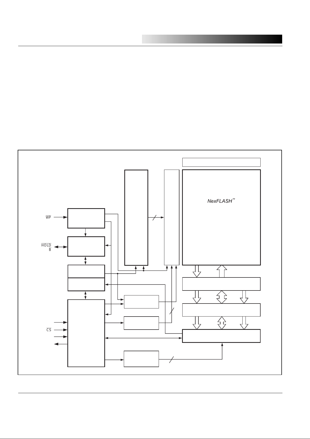
FUNCTIONAL OVERVIEW
The
NexFLASHTM
IS25F011A, IS25F021A, and
IS25F041A Serial Flash memories provide up to 1M-bit,
2M-bit, and 4M-bit respectively, of low-power and lowvoltage nonvolatile memory that is fully accessible through
a 4-pin Serial Peripheral Interface (SPI) bus. The
IS25F011A, IS25F021A, and IS25F041A incorporate a
variety of special features, such as on-board Serial SRAM,
advanced write protection, and electronic device identification.
DEVICE INFORMATION SECTOR
WRITE PROTECT LOGIC
1, 2, or 4 MEGABIT
SERIAL FLASH MEMORY ARRAY
512, 1024, OR 2048 BYTE-ADDRESSABLE
SECTORS OF 264 BYTES EACH
ROW DECODE (512, 1024, OR 2048 SECTORS)
PROGRAM BUFFER
(264 BYTES)
2112
2112
8
8
8
SRAM
(264 BYTES)
COLUMN DECODE, SENSE AMP LATCH
AND DATA COMPARE LOGIC
HIGH-VOLTAGE
GENERATORS
SECTOR-ADDRESS
LATCH
DATA
9/10/11
WRITE CONTROL
LOGIC
WP
HOLD OR
READ/BUSY
LOGIC
CONFIGURATION
REGISTER
STATUS
REGISTER
SPI
COMMAND
AND
CONTROL
LOGIC
BYTE-ADDRESS
LATCH/COUNTER
9
16
HOLD
OR R/
B
SCK
CS
SI
SO
Figure 2. IS25F011A, IS25F021A, and IS25F041A Architectural Block Diagram
An architectural block diagram of the IS25F011A,
IS25F021A, and IS25F041A is shown in Figure 2. Key
elements of the architecture include:
• SPI Interface and Command Set Logic
• Serial Flash Memory Array
• Serial SRAM and Program Buffer
• Write Protection Logic
• Configuration and Status Registers
Page 3
IS25F011A
IS25F021A
IS25F041A
Integrated Silicon Solution, Inc.
3
PRELIMINARY SF001-1A
06/24/98
1
2
3
4
5
6
7
8
9
10
11
12
ISSI
®
Figure 3. IS25F011A, IS25F021A, and IS25F041A
Pin Assignments, 28-Pin TSOP (Type I)
HOLD-R/B
NC
WP
NC
NC
VCC
GND
NC
NC
NC
CS
SCK
SI
SO
NC
NC
NC
NC
NC
NC
NC
NC
NC
NC
NC
NC
NC
NC
1
2
3
4
5
6
7
8
9
10
11
12
13
14
28
27
26
25
24
23
22
21
20
19
18
17
16
15
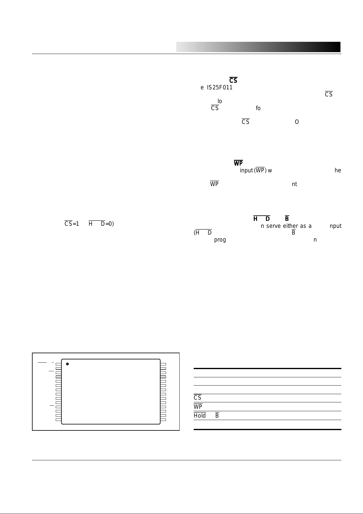
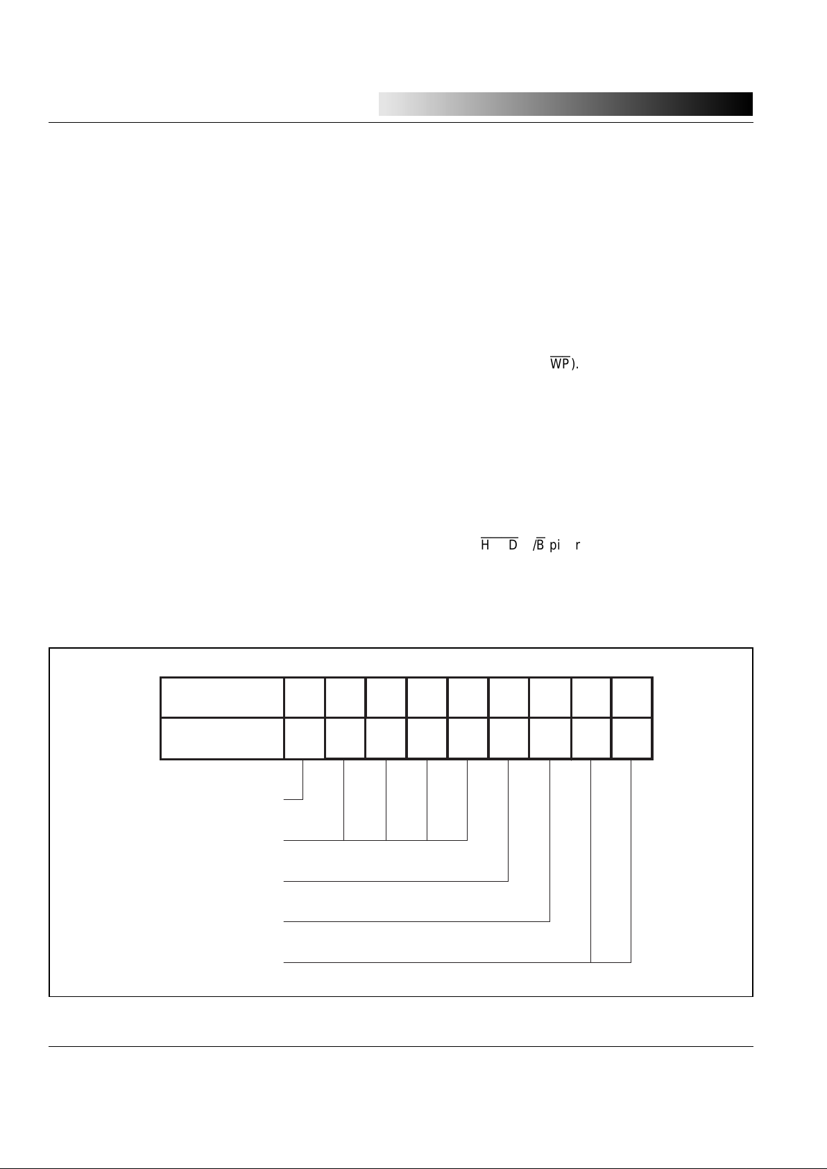
Table 1. Pin Descriptions
SI Serial Data Input
SO Serial Data Output
SCK Serial Clock Input
CS
Chip Select Input
WP
Write Protect Input
Hold
, R/
B
Hold Input or Read Busy Output
Vcc Power Supply
Pin Descriptions
Package
The IS25F011A, IS25F021A, and IS25F041A are
available in a 28-pin TSOP (Type I) surface mount
package. See Figure 3 and Table 1 for pin assignments. All interface and supply pins are on one
side of the package. The “No Connect” (NC) pins
are not connected to the device, allowing the pads
and the area around them to be used for routing PCB
system traces. The devices are also available in a
cost-effective and space-efficient removable Serial
Flash Module package.
Serial Data Imput (SI)
The SPI bus Serial Data Input (SI) provides a means
for data to be written to (shifted into) the device.
Serial Data Output (SO)
The SPI bus Serial Data Output (SO) provides a
means for data to be read from (shifted out of) the
device during a read operation. When the device is
deselected (CS=1 or
HOLD
=0) the SO pin is in a
high-impedance state.
Serial Clock (SCK)
All commands and data written to the Serial Input
(SI) are clocked relative to the rising edge of the
Serial Clock (SCK). All data read from the Serial
Data Output (SO) is clocked relative to the falling or
rising edge of SCK as specified in the nonvolatile
configuration register. The data output clock edge is
factory-programmed to the default condition of the
falling edge, allowing compatibility with standard
SPI systems. Clock rates of up to 16 MHz for 5V
devices and up to 8 MHz for 3V devices are supported.
Chip Select (
CSCS
CSCS
CS
)
The IS25F011A, IS25F021A, and IS25F041A are selected for operation when the Chip Select input (CS) is
asserted low. Upon power-up, an initial low-to-high transition of CS is required before any command sequence will
be acknowledged. The device can be deselected to a nonactive state when CS is brought high. Once deselected,
the SO pin will enter a high-impedance state and power
consumption will decrease to standby levels unless programming is in process, in which case standby will resume
when programming is complete.
Write Protect (
WPWP
WPWP
WP
)
The Write Protect input (WP) works in conjunction with the
write protect range set in the configuration register bits.
When WP is asserted (active low) the entire Flash memory
array is write protected. When high, any Flash memory
sector can be written to unless its address is within the
write protect range that is set in the configuration register.
Hold or Ready/Busy (
HOLDHOLD
HOLDHOLD
HOLD
or R/
BB
BB
B
)
This multi-function pin can serve either as a Hold input
(
HOLD
) or as a Ready-Busy output (R/B). The pin function
is user-programmable via the nonvolatile configuration
register. Factory-programmed as a no-connect, the pin
can be reconfigured as a Ready-Busy output or as a Hold
input by setting the configuration register. See the configuration register section of this data sheet for further details.
Power Supply Pins (Vcc and GND)
The IS25F011A, IS25F021A, and IS25F041A support
single power supply Read and Erase/Write operations in
5V (4.5V -5.5V) and 3V (2.7V-3.6V) Vcc versions. Typical
active power is as low as 5 mA for the 3V version with
standby current less than 1 µA.
Page 4
IS25F011A
IS25F021A
IS25F041A
4
Integrated Silicon Solution, Inc.
PRELIMINARY SF001-1A
06/24/98
ISSI
®
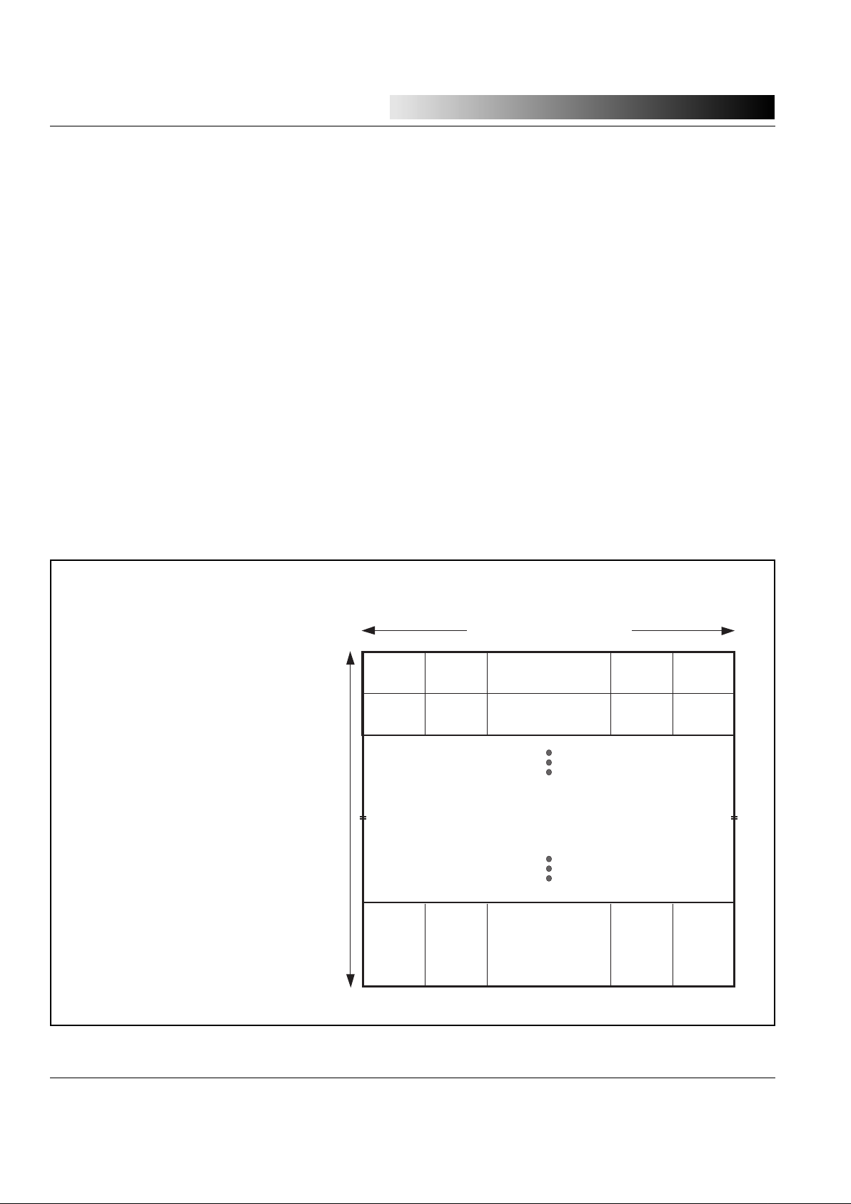
Serial Flash Memory Array
The IS25F011A, IS25F021A, and IS25F041A Serial Flash
memory arrays are organized as 512, 1024, and 2048
sectors of 264-bytes (2,112 bits) each, as shown in Figure
4. Grouping sectors as pairs offer a convenient format for
applications that store and transfer data in a DOS compatible sector size of 512-bytes. The additional 16-bytes per
sector pair can be used for sector management such as
header, checksum, CRC, or other related application
requirements.
The Serial Flash memory of the IS25F011A, IS25F021A,
and IS25F041A is byte-addressable. That is, each sector
is individually addressable and each byte within a sector
is individually addressable. This allows a single byte, or
specified sequence of bytes, to be read without having to
clock an entire 264-byte sector out of the device. Data can
be read directly from a sector in the Flash memory array
by using a
Read from Sector
command from the SPI bus.
Data can be written to a sector in the Flash memory array
by means of the Serial SRAM using a
Write to Sector
command or a
Transfer SRAM to Sector
command.
After a sector has been written, the memory array will
become busy while it is programming the specified nonvolatile memory cells of that sector. This busy time will not
exceed tWP (~5 ms for 5V devices), during which time the
Flash array is unavailable for read or write access. The
device can be tested to determine the array’s availability using the Ready/Busy status that is available during
most read commands, via the status register, or on the
Ready/Busy pin. Note that the SRAM is always available,
even when the memory array is busy. See the Serial
SRAM section for more details.
The IS25F011A, IS25F021A, and IS25F041A do not
require pre-erase. Instead, the device incorporates an
auto-erase-before-write feature that automatically erases
the addressed sector at the beginning of the write operation. This allows for fast and consistent programming
times. It also simplifies firmware support by eliminating
the need for a separate pre-erase algorithm and the
complex management of disproportional erase and write
block sizes commonly found in other devices.
Byte 0
000H
Sector 0
000H
25F021
S[9:0]
25F011
S[8:0]
25F041
S[10:0]
Sector Address:
Byte Address: B[8:0]
Sector 1
001H
Sector 2047
7FFH
Sector 1023
3FFH
Sector 511
1FFH
Sector 2046
7FEH
Sector 1022
3FEH
Sector 510
1FEH
Sector 2-2045
002H-7FDH
Sector 2-1021
002H-3FDH
Sector 2-509
002H-1FDH
Byte1
001H
Byte1
001H
Byte 2-261
002H-105H
Byte 2-261
002H-105H
1M-bit, 2M-bit, or 4M-bit Serial Flash Memory Array
512, 1024, and 2048 Byte-Addressable Sectors
of 264-Bytes each
Byte 262
106H
Byte 262
106H
Byte 263
107H
Byte 0
000H
Byte 263
107H
Byte 0
000H
Byte 0
000H
Byte 1
001H
Byte 1
001H
Byte 2-261
002H-105H
Byte 2-261
002H-105H
Byte 262
106H
Byte 262
106H
Byte 263
107H
Byte 263
107H
Sector 1
001H
Sector 1
001H
Sector 0
000H
Sector 0
000H
Figure 4. IS25F011A, IS25F021A, and IS25F041A Serial Flash Memory Array
Page 5
IS25F011A
IS25F021A
IS25F041A
Integrated Silicon Solution, Inc.
5
PRELIMINARY SF001-1A
06/24/98
1
2
3
4
5
6
7
8
9
10
11
12
ISSI
®
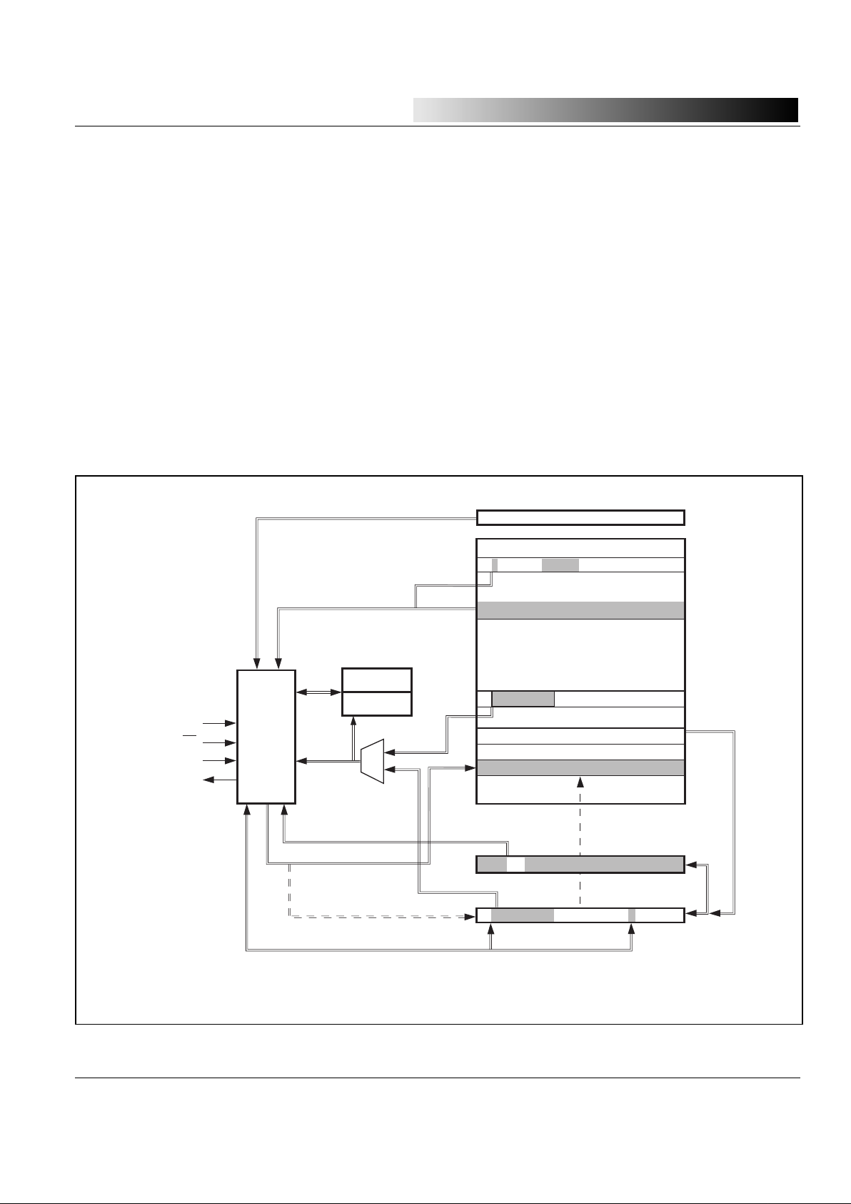
Serial SRAM and Program Buffer
One of the most powerful features of the IS25F011A,
IS25F021A, and IS25F041A is the integrated Serial
SRAM and its associated Program Buffer. Together, the
264-byte Serial SRAM and 264-byte Program Buffer
provide up to 528-bytes of usable SRAM storage. The
SRAM can be used in conjunction with the Flash memory
or independently.
The main purpose of the Serial SRAM is to serve as the
primary buffer for sector data to be written into the Serial
Flash memory array. Using the
Write to Sector
command,
data is first shifted into the SRAM from the SPI bus. When
the command sequence has been completed, the entire
264-bytes is transferred to the Program Buffer. The Program Buffer supports the array during the Erase/Write cycle
(tWP), freeing the SRAM to accept new data. This double-
buffering scheme increases erase/write transfer rates and
can eliminate the need for external RAM buffers (Figure 5).
The SRAM is fully byte-addressable. Thus, the entire
264-bytes, a single byte, or a sequence of bytes can be
read from, or written to the SRAM. This allows the SRAM
to be used as a temporary work area for read-modify-write
operations prior to a sector write.
The
Transfer Sector to SRAM
command allows the contents of a specified sector of Flash memory to be moved to
the SRAM. This can be useful when only a portion of a
sector needs to be altered. In this case the sector is first
transferred to the SRAM, where modifications are made
using the
Write to SRAM
command. Once complete, a
Transfer SRAM to Sector
command is used to update the
sector.
SPI
COMMAND
AND
CONTROL
LOGIC
SCK
CS
SI
SO
STATUS
REGISTER
CONFIGURATION
REGISTER
PROGRAM BUFFER
COMPARE SECTOR
TO SRAM
READ FROM
DEVICE INFORMATION
SECTOR
READ FROM
PROGRAM BUFFER
Note:
1. A single byte, several bytes, or all bytes of a Flash sector, the SRAM, or Program Buffer may be addressed.
2. All double lines represent implied connections or actions.
SERIAL FLASH MEMORY ARRAY
512, 1024, AND 2048 BYTE-ADDRESSABLE
SECTORS OF 264-BYTES EACH
DEVICE INFORMATION SECTOR
TRANSFER SRAM TO SECTOR
(VIA PROGRAM BUFFER)
WRITE TO SECTOR
(VIA SRAM &
PROGRAM BUFFER)
TRANSFER SRAM TO
PROGRAM BUFFER
TRANSFER PROGRAM
BUFFER TO SRAM
SERIAL SRAM
READ FROM
OR WRITE TO
SRAM
TRANSFER
SECTOR TO
SRAM
READ FROM
SECTOR
Figure 5. Command Relationships of the SPI Interface, Serial Flash Memory Array, SRAM, and Program Buffer
Page 6
IS25F011A
IS25F021A
IS25F041A
6
Integrated Silicon Solution, Inc.
PRELIMINARY SF001-1A
06/24/98
ISSI
®
CF15:9
(RESERVED)
CF8 CF7 CF6 CF5 CF4 CF3 CF2 CF1 CF0
AF WR3 WR2 WR1 WR0 WD RCE HR1 HR0
ALTERNATE OSCILATOR
FREQUENCY
WRITE PROTECT
RANGE
WRITE PROTECT
DIRECTION
READ DATA
CLOCK EDGE
HOLD-READY/BUSY
PIN FUNCTION
Figure 6. Configuration Register Bit Locations
The
Compare Sector
command allows the contents of the
SRAM to be compared with the specified sector in memory.
The result of the compare is set in the status register. This
command can be useful when rewriting multi-sector files
that have only minor changes from the previous write. If the
new data in the SRAM is the same as the previously
written data, the sector write can be skipped. Used in this
way, the command saves time that would have been
used for re-programming. It also extends the endurance
of the Flash memory cells. The Compare Sector command
is also useful for write/verify operation (see High Data
Integrity Applications, page 19).
Using the SRAM Independant of Flash Memory
The SRAM can be used independently of Flash memory
operations for lookup tables, variable storage, or scratch
pad purposes. If the Flash memory needs to be written to
while SRAM is being used for a different purpose, the
contents can be temporarily stored to a sector and then
transferred back again when needed. The SRAM can be
especially useful for RAM-limited microcontroller-based
systems, eliminating the need for external SRAM and
freeing pins for other purposes. It can also make it possible
to use small pin-count microcontrollers, since only a few
pins are needed for the interface instead of the 20-40 pins
required for parallel bus-oriented Flash devices.
If more than 264 bytes of SRAM are needed, the
Transfer
SRAM to Program Buffer, Transfer Program Buffer to
SRAM
, and the
Read Program Buffer
commands can be
used to expand the storage to 528 bytes. In this mode of
operation, all writes must be handled through the 264-byte
SRAM and the Program buffer is essentially used as a
stack.
Write Protection
The IS25F011A, IS25F021A, and IS25F041A provide
advanced software and hardware write protection features. Software-controlled write protection of the entire
array is handled using the
Write Enable and Write Disable
commands. Hardware write protection is possible using
the Write Protect pin (WP). Write-protecting a portion of
Flash memory is accommodated by programming a write
protect range in the configuration register. For applications needing a portion of the memory to be permanently
write-protected, a onetime programmable write protection feature is supported. Contact
ISSI
for further informa-
tion.
Configuration Register
The Configuration Register stores the current configuration of the
HOLD
-R/B pin, read clock edge, write protect
range, and alternate oscillator frequency (Figure 6). The
configuration register is accessed using the
Write and
Read Configuration Register
commands. A nonvolatile
Page 7
IS25F011A
IS25F021A
IS25F041A
Integrated Silicon Solution, Inc.
7
PRELIMINARY SF001-1A
06/24/98
1
2
3
4
5
6
7
8
9
10
11
12
ISSI
®
register, the configuration register will maintain its setting
even when power is removed. The factory default setting
for bits CF8-CF0 is: 0 0000 1001 B(write protect range =
none, read uses falling edge of the clock, and pin 1 = no
connect). Bits CF15-CF9 are reserved. When writting to
the configuration register CF15-CF9 should be 0. When
reading, the settings of CF15-CF9 should be ignored.
Standard write endurance rating of the memory array
allows for 10,000 erase/write cycles. Extended endurance to 100,000 cycles is possible using ECC techniques
like those provided in the SFK-SPI Development Kit (see
High Data Integrity Application, page 19). The rating of the
configuration register EEPROM cells, however, is 1,000
write cycles. This is more than adequate considering the
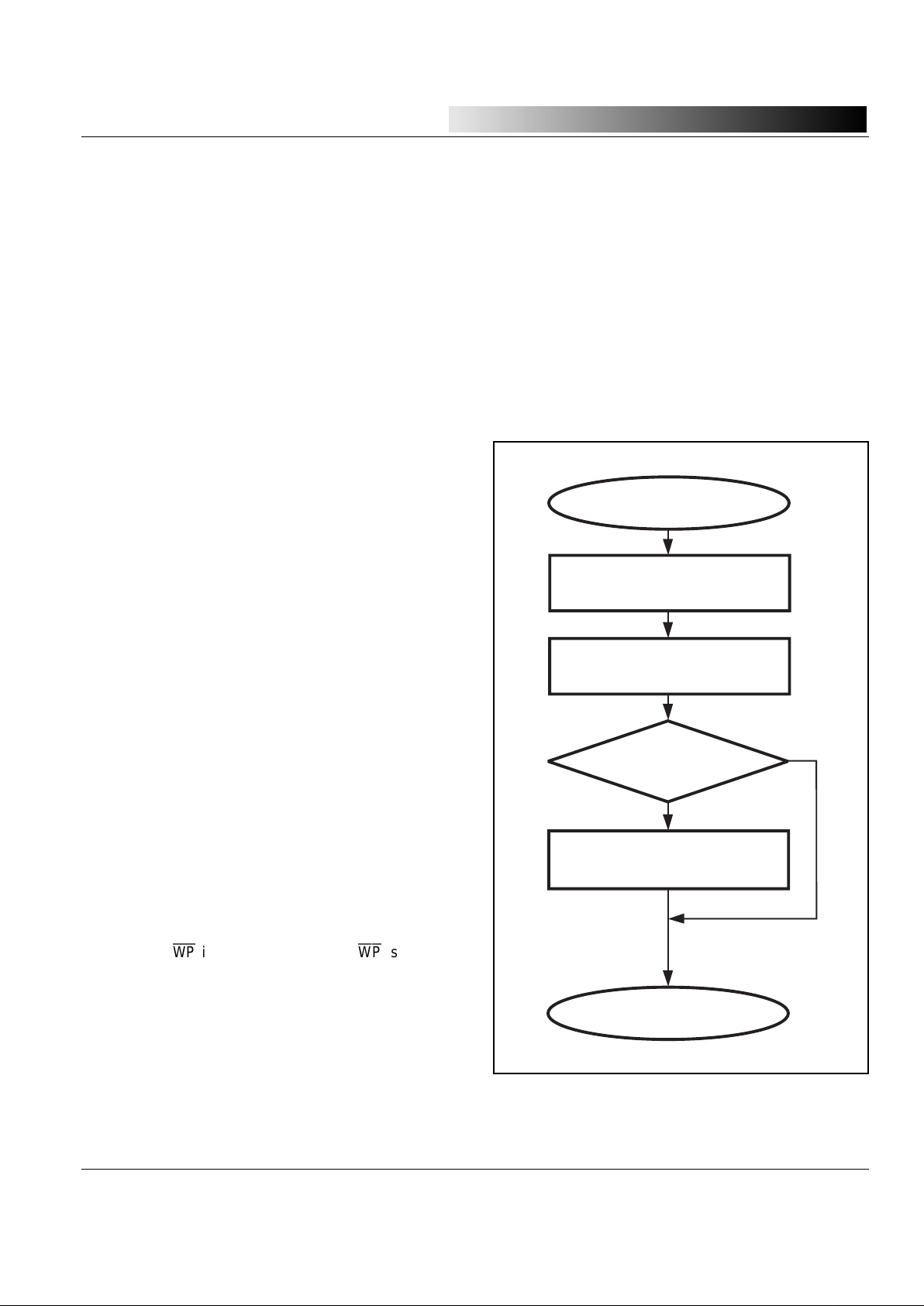
configuration seldom needs to be changed. To minimize
writes to the configuration register, the configuration
register should be read upon power-up to determine if a
change is required. If no change is needed, the write
configuration command can be skipped. This process will
extend the life of the configuration register and save
processing time (Figure 7).
Alternate Oscillator Frequency, AF
Flash memory devices have charge pump oscillators to
generate internal high-voltages used for programming
nonvolatile memory cells. In some applications, the oscillator frequency of the charge pump may cause noise
interference. To solve this problem, an alternate oscillator frequency (AF) can be selected by setting bit CF[8]
of the configuration register. The alternate frequency is
a non-harmonic frequency of the standard oscillator. The
factory default setting is for the standard oscillator frequency, AF equal to 0.
AF=0 Standard Oscillator Frequency is used.
AF=1 Alternate Oscillator Frequency is used.
Write Protect Range and Direction, WR[3:0], WD
The write protect range and direction bits WR[3:0] and
WD are located at configuration bits CF[7:4] and CF[3]
respectively. The write protect range and direction bits
select how the array is protected. They work in conjunction with the WP input pin, valid only if WP is inactive
(high). WR[3:0] can select write protection of all sectors,
none of the sectors, or specific sectors grouped in blocks
of 32 (~8 KB). The WD bit specifies whether the protected
block range starts from the first sector, address 0 (000H),
or from the last sector (1FFH for the IS25F011A, 3FFH for
the IS25F021A, and 7FF for the IS25F041A). Table 2 lists
the write protect sector range for both devices. Once
protected, all further writes to sectors within the range will
be ignored . The factory default setting is with no write
protected sectors, WR=[0,0,0,0] and WD=1.
Read Clock Edge, RCE
The Read Clock Edge bit (RCE) is located at configuration bit location CF[2]. It selects which edge of the clock
(SCK) is used while reading data out of the device.
Although the SPI protocol specifies that data is written
during the rising edge and read on the falling edge of the
clock, if required, the output can be driven on the rising
edge of the clock by setting the configuration registers
RCE bit to a 1. Using the rising edge of clock for data
reads may be beneficial to the timing of some high-speed
systems. The factory default setting is the falling edge of
SCK.
RCE=0 Read data is output on the falling edge of SCK.
RCE=1 Read data is output on the rising edge of SCK.
Figure 7. Flow Chart for Checking the Configuration
Register upon Power-up
System Power-up
Read Device Information Sector,
Verify Device Density and Type
Read Configuration Register
Verify bits are Set as Needed
Configuration
Setting is Correct?
Yes
Write Configuration Register
to Correct Setting
Application Routines
No
Page 8

IS25F011A
IS25F021A
IS25F041A
8
Integrated Silicon Solution, Inc.
PRELIMINARY SF001-1A
06/24/98
ISSI
®
HOLDHOLD
HOLDHOLD
HOLD
-R/
BB
BB
B
, HR[1:0]
The Hold-Ready/Busy (
HOLD
-R/B) bits HR1 and HR0 are
located at bits CF[1:0] of the configuration register. These
two bits select one of four possible functions: No Connect,
HOLD
input, R/B Output, or R/B Output with open drain. The
factory setting for the pin is “No Connect”.
HR1 HR0 Pin Configuration
00
HOLD
input
0 1 No Connect
10R/
B
Output (Open Drain)
11R/
B
Output
Configured as a R/B output, the pin can serve as a system
interrupt. When R/B is high, the array is ready to be
programmed. When R/B is low, it is busy programming.
If configured with an open-drain, an external pull-up
resistor should be used.
As a
HOLD
input, the pin can be used in conjunction with
the CS and SCK pin to suspend a serial command
sequence without resetting the command. This can be
useful if a command is in process and a higher priority
task on the same SPI bus needs to be attended to. To
suspend a command,
HOLD
must be brought low while
CS
and SCK are low. With
HOLD
low, further data on the
SI pin is ignored (even while SCK is clocked) and the SO
pin goes to a high-impedance state. To resume the
command sequence,
HOLD
must be brought high when
CS
and SCK are low. See timing diagrams.
Status Register Bit Descriptions
The status register provides status of the Flash array’s
Ready/Busy condition (R/B), transfers between the SRAM
and program buffer (TX), Write-Enable/Disable (WE),
and Compare Not Equal (CNE). The register can be read
using the Read Status Register command (Figure 8).
Ready/Busy Status, BUSY
The BUSY status bit is located at bit ST[7] of the status
register. Testing the BUSY bit is one of several ways to
check Ready/Busy status of the array. At power-up the
BUSY bit is reset to 0.
BUSY=1 The memory array is busy programming.
BUSY=0 The memory array is ready for further use.
SRAM and Program Buffer Transfer, TR
The TR status bit is located at bit ST[6] of the status
register. The bit provides status primarily for use during
the
Transfer SRAM to Program Buffer
command and
Transfer Program Buffer to SRAM
command. An active
state 1 indicates a transfer is in process and the SRAM
or Program Buffer is not available for use. The device
will indicate a BUSY state while the TR bit is active.
Upon power up the TR bit resets to 0.
TR=1 SRAM and Program Buffer Transferring.
TR=0 SRAM and Program Buffer Not Transferring.
Write Enable/Disable, WE
The WE status bit is located at bit ST[4] of the status
register. The bit provides write protect status of global
Write Enable and Write Disable
commands. Upon power-
up the WE bit resets to 0.
WE=1 Write Enabled, array can be written to.
WE=0 Write Disabled, array can not be written to.
Table 2. Write Protect Range Sector Selection (Hex)
Write Protect
Range Config. Bits Write Protected Sectors
WR3 WR2 WR1 WR0 WD=0 WD=1
0 0 0 0 None None
0 0 0 1 000 - 01FH x E0 - 1FF/ 3FF/ 7FFH
0 0 1 0 000 - 03FH x C0 - 1FF/ 3FF/ 7FFH
0 0 1 1 000 - 05FH x A0 - 1FF/ 3FF/ 7FFH
0 1 0 0 000 - 07FH x 80 - 1FF/ 3FF/ 7FFH
0 1 0 1 000 - 09FH x 60 - 1FF/ 3FF/ 7FFH
0 1 1 0 000 - 0BFH x 40 - 1FF/ 3FF/ 7FFH
0 1 1 1 000 - 0DFH x 20 - 1FF/ 3FF/ 7FFH
1 0 0 0 000 - 0FFH x 00 - 1FF/ 3FF/ 7FFH
1 0 0 1 000 - 11FH y E0 - 1FF/ 3FF/ 7FFH
1 0 1 0 000 - 13FH y C0 - 1FF/ 3FF/ 7FFH
1 0 1 1 000 - 15FH y A0 - 1FF/ 3FF/ 7FFH
1 1 0 0 000 - 17FH y 80 - 1FF/ 3FF/ 7FFH
1 1 0 1 000 - 19FH y 60 - 1FF/ 3FF/ 7FFH
1 1 1 0 000 - 1BFH y 40 - 1FF/ 3FF/ 7FFH
1 1 1 1 ALL ALL
Note:
1. IS25F041A x=7 Y=6, IS25F021A x=3 y=2,
and IS25F011A x=1 y=0
Page 9

IS25F011A
IS25F021A
IS25F041A
Integrated Silicon Solution, Inc.
9
PRELIMINARY SF001-1A
06/24/98
1
2
3
4
5
6
7
8
9
10
11
12
ISSI
®
Busy TR
ST7XST6WEST5XST4
CNE
ST3XST2XST1 ST0
x =
RESERVED
READ/BUSY
SRAM AND PROGRAM
BUFFER TRANSFER
FLASH ARRAY WRITE
ENABLE/DISABLE
SECTOR-SRAM
COMPARE NOT EQUAL
Figure 8. Status Register Bit Locations
Compare Not Equal, CNE
The CNE status bit is located at bit ST[3] of the status
register. The bit provides a cumulative comparison result
during a
Compare Sector with SRAM
command. The CNE
bit is reset to a 0 upon power-up or after a Clear Compare
Bit command is executed.
CNE=1 Sector and SRAM contents are not equal.
CNE=0 Sector and SRAM are equal or CNE bit reset.
Command Set
The IS25F011A, IS25F021A, and IS25F041A have a
powerful command set that is fully controlled through the
SPI bus. Command relations are shown in Figure 5 and
a list of commands and their associated address, status,
clock, and data bytes are shown in Table 3. Detailed
clock timing of the
Read Sector
and
Write Sector
com-
mand sequences are shown in Figures 10 and 11.
After power up, a device enters an idle state that will
maintain until CS pin is asserted low. All commands are
entered from the SPI serial data input (SI) pin on the rising
edge of SCK while CS is asserted low. All command,
address, and configuration bits are shifted into the device
with most-significant-bit-first. Data bits read from the
device are shifted out with least significant byte first
(i.e., byte-00H, byte-01H,...). The bit order within each
byte is most-significant-bit first (i.e.,D7,...D0). All commands are completed by asserting the CS pin high.
Note that the entire 264-byte contents of a Flash sector,
the SRAM, or Program Buffer does not have to be
accessed all at once. Read, Write, Transfer, and Compare commands allow for byte addressing. Thus a single
byte, or clocked sequence of bytes, can be accessed at
any starting location within the 264-byte boundary as
specified by the byte-address field.
Page 10

IS25F011A
IS25F021A
IS25F041A
10
Integrated Silicon Solution, Inc.
PRELIMINARY SF001-1A
06/24/98
ISSI
®
00000000
C[7:0] Command
S[15:0] Sector Address
B[15:0] Byte Address
RB[15:0] Ready/Busy Status (9999H=Ready)
High-Z
SO Output is Driven
1
st Byte of Data
2nd Byte of Data
16 Clocks
High-Z
Last Byte of Data
n-Bytes of Data
Idle
CS
SCK
SI
SCK
SI
SO
SCK
SO
CS
SCK
SO
C7 C6 C5 C4 C3 C2 C1 C0 0 0 0 0
0
S10
S9 S8 S7 S6 S5 S4 S3 S2 S1 S0
0 0 0 0 0 0 0 B8 B7 B6 B5 B4
B3 B2 B1 B0 0 0 0 0 0 0 0 0
10011001100110
0 1 D7 D6 D5 D4 D3 D2 D1 D0 D7 D6 D4 D5
D3 D2 D1 D0
D7 D6 D5 D4 D3 D2 D1 D0
Idle
Figure 10. Read from Sector Command Sequence
D7 D6 D5 D4 D3 D2 D1 D0
C[7:0] Command
S[15:0] Sector Address
B[15:0] Byte Address
Last Byte of Data
n-Bytes of Data
t
WP
Program Time
CS
SCK
SI
SCK
SI
CS
SCK
SI
C7 C6 C5 C4 C3 C2 C1 C0 0 0 0 0
0
S10
S9 S8 S7 S6 S5 S4 S3 S2 S1 S0
0 0 0 0 0 0 0 B8 B7 B6 B5 B4
B3 B2 B1 B0 D7 D6 D5 D4 D3 D2 D1 D0
Idle
1
st Byte of Data
2nd Byte of Data
D7 D6 D5 D4 D3 D2 D1 D0 0 0 0 0 0 0 0 0
8 Clocks
Figure 11. Write to Sector Command Sequence
Page 11

IS25F011A
IS25F021A
IS25F041A
Integrated Silicon Solution, Inc.
11
PRELIMINARY SF001-1A
06/24/98
1
2
3
4
5
6
7
8
9
10
11
12
ISSI
®
SERIAL FLASH SECTOR COMMANDS
Read From Sector
Reading from a sector is accomplished by first bringing
CS
low then shifting in the
Read from Sector
command
(52H) followed by its 16-bit “sector-address” field. Although the sector-address field is 16-bits, only bits
S[8:0] for the IS25F011A (0-1FFH), S[9:0] for the
IS25F021A (0-3FFH), S[10:0] for the IS25F041A
(0-7FFH) are used. The uppermost sector address bits
are not used but must be clocked using 0 for data. Next
a 16-bit “byte-address” field is clocked into the device
to designate the starting location within the 264-byte
sector. Only B[8:0] of the byte-address field are used;
the uppermost bits are not used but must be clocked in
(use 0 for data). Only byte-addresses of 0 to 107H
(264 bytes) are valid.
Table 3. Command Set for the IS25F011A, IS25F021A, and IS25F041A Serial Flash Memory
n - bytes
Command Name Byte 0 Byte 1-2 Byte 3-4 (
italics indicate device output
)
Serial Flash Sector Commands
Read from Sector 52H sector addr. byte add. 0000H
ready/busy read data
Read from Sector Low Frequency 51H sector addr. byte add. 0000H
ready/busy read data
Write Enable* 06H 00H
Write Disable* 04H 00H
Write to Sector F3H sector addr. byte add. write data 00H
Transfer SRAM to Sector F3H sector addr. 0000H
Transfer Sector to SRAM 54H sector addr. byte add. clock 00H per byte 00H
Compare Sector with SRAM 86H sector addr. byte add. 0000H
ready/busy bit compare of data
Serial SRAM Program Buffer Commands
Write to SRAM** 82H 0000H byte add. write data 00H
Read from SRAM* 81H 0000H byte add. 0000H
read/busy read data
Transfer SRAM to Prog. Buffer 92H 0000H 0000H 0000H
Transfer Prog. Buffer to SRAM 55H 0000H 0000H 0000H
Read from Program Buffer 91H 0000H byte add. 0000H
ready/busy read data
Configuration and Status Commands
Read Configuration Register* 8BH 0000H 0000H 0000H
ready/busy configuration
Write Configuration Register 8AH configuration 0000H
Read Status Register* 83H 0000H 0000H 0000H
ready/busy status
Clear Compare Sector* 89H 0000H
Read Device Information Sector 15H 0000H byte add. 0000H
ready/busy read data
Notes:
1. * Command may be used when device is busy
2. ** Command may not be used when device is busy and TR bit=0
Page 12

IS25F011A
IS25F021A
IS25F041A
12
Integrated Silicon Solution, Inc.
PRELIMINARY SF001-1A
06/24/98
ISSI
®
Write Enable
Command
8 Clocks
SI
06H 00H
SO
Write Enable
Upon power-up, the Flash memory array is write- protected until the
Write Enable
command (06H) has been
issued. The WP pin must be inactive while writing the
command for the write enable to be accepted. The status
of the device’s write protect state can be read in the status
register. The
Write Enable
command sequence is com-
pleted by asserting CS high after eight additional clocks.
Read from
Sector
Command
Sector
Address*
Byte
Address** 16 Clocks
SI
SO
52H S[15:0] B[15:0] 0000H
RB[15:0] First Byte - Last Byte
Read/Busy
Status
Read Sector Data
*The sector address only uses bits [8:0], [9:0] or [10:0]
**The byte address only uses bits [8:0]
Following the byte-address field, 16 control clocks are
required with data=0. The Serial Data Output (SO) will
change from a high-impedance state and begin to drive
the output with Ready/Busy status RB[15:0]. If SO uses
the rising edge of clock (configuration register RCE=1),
the output will be driven after the last control clock. If
SO uses the falling edge of clock (RCE=0), the output
will be driven on the next falling edge of clock. If the
array is not busy, the output status will be 9999H,
followed by the sector data on the SO pin. If the array
is busy, the status will be 6666H, and the command
should be terminated and restarted after a ready state
occurs. The data field is shifted out with the least
significant byte first (i.e., byte-00H, byte-01H, ...). The
bit order within each byte is the most significant bit first
(i.e.,D7,...D0). The byte-address is internally incre-
mented to the next higher byte address as the clock
continues. When the highest byte-address (107H) is
reached, the address counter rolls over to byte-0H and
continues to increment. Asserting the CS pin high
completes (or terminates) the command. Detailed timing for the
Read from Sector
command is shown in
Figure 10.
Read Sector (Low Frequency)
The
Read Sector at Low Frequency
command (51H) can
reduce power consumption during read operations by
25%-40% when the system clock frequency is 1 MHz or
lower. The command sequence is identical to the standard
Read from Sector
command.
Write Disable
Command
8 Clocks
SI
04H 00H
SO
Write Disable
The
Write Disable
command (04H) protects the Flash
memory array from being programmed. Once issued,
further
Write to Sector or Transfer SRAM to Sector
commands will be ignored. The status of the write protect state
can be read in the status register. The
Write Disable
command sequence is completed by asserting CS high
after eight additional clocks.
Page 13

IS25F011A
IS25F021A
IS25F041A
Integrated Silicon Solution, Inc.
13
PRELIMINARY SF001-1A
06/24/98
1
2
3
4
5
6
7
8
9
10
11
12
ISSI
®
The bit order within each byte is most significant bit first
(i.e., D7,...D0). The byte-address is automatically incremented to the next higher byte address as the clock
continues. When the last byte address to be written is
reached, the command can be completed with an
additional eightcontrol clocks (with data=0) followed by
asserting
CS
high. If the clock continues to increment
past the highest byte-address (107H), the address
counter will roll over to byte 0H.
After the CS pin is brought high, the data in the SRAM
is automatically transferred to the Program Buffer, which
handles the self-timed programming of the specified
sector in memory array. See tWP timing specifications.
During this time the array will be “busy” and will ignore
further array-related commands until complete. All
Ready/Busy status indicators will indicate a busy status. Since the Program Buffer handles all array programming, the SRAM is still available to be read from or
written to during the busy state. Applications that require
high data integrity should verify written sectors or use other
techniques such as ECC (see High Data Integrity Applications, page 19). Detailed clock timing for the
Write to
Sector
command is shown in Figure 11.
Write to Sector
Before writing to a sector in the Flash memory array, all
hardware and software write protection must be in an
enabled state. This means that the WP pin must be in a
high state, a
Write Enable
command must have previously been issued, and the sector location that is to be
written to must be outside the write protect range set in
the configuration register. Additionally, the Ready/Busy
status should be checked to confirm that the memory
array is available to be written to.
Writing to a sector is accomplished by first bringing
CS
low and shifting in the
Write to Sector
command (F3H)
followed by a 16-bit “sector-address” field. Although the
sector-address field is 16-bits, only bits S[8:0] for the
IS25F011A (0-1FFH), S[9:0] for the IS25F021A (0-3FFH),
or S[10:0] for the IS25F041A (0-7FFH) are used. The
uppermost sector address bits are not used but must be
clocked in (use 0 data). Following the sector address, a
16-bit “byte-address” field is clocked into the device to
designate the starting location within the 264-byte sector.
Only bits B[8:0] of the byte-address field are used and
only values of 0-107H (264 bytes) are valid.
After the byte-address has been loaded, data is shifted
into the 264-byte SRAM, which serves as a temporary
storage buffer. Existing data in the SRAM will be written
over. The byte order of the data shifted into the SRAM
is least significant byte first (i.e., byte-00H, byte-01H,...).
Write to
Sector
Command
8 Clocks
SI
F3H
S[15:0] B[15:0] First Byte - Last Byte 00H
SO
Sector
Address*
Byte
Address**
Write Sector Data
*The sector address only uses bits [8:0], [9:0] or [10:0]
**The byte address only uses bits [8:0]
Program
Time
(
t
WP
)
Transfer SRAM to Sector
The
Transfer SRAM to Sector
command (F3H) will
write the existing contents of the SRAM to the specified sector in memory. The command sequence is
identical to that of the
Write to Sector
command
except that immediately after the sector address field
S[15:0] and 16 control clocks, the CS pin is asserted
high. This automatically transfers the 264-bytes of
SRAM data to the Program Buffer, which handles the
programming of the specified sector in the memory
array. During this time, the array will be busy. Since the
entire 264-bytes are transferred, the byte-address field
B[15:0] is not used.
Transfer SRAM
to Sector
Command
Sector
Address*
16 Clocks
SI
SO
F3H S[15:0] 0000H
*The sector address only uses bits [8:0] or [10:0]
Program Time
(
t
WP
)
Page 14

IS25F011A
IS25F021A
IS25F041A
14
Integrated Silicon Solution, Inc.
PRELIMINARY SF001-1A
06/24/98
ISSI
®
Compare Sector
with SRAM
Command
Sector
Address*
Byte
Address** 16 Clocks
SI
SO
86H S[15:0] B[15:0] 0000H
RB[15:0] First Byte - Last Byte
Read/Busy
Status
Bit Compare of Sector
and SRAM
*The sector address only uses bits [8:0], [9:0] or [10:0]
**The byte address only uses bits [8:0]
Compare Sector to SRAM
The
Compare Sector to SRAM
command does a bit-by-bit
comparison of the data stored in the addressed sector
against data in the SRAM. The command is similar to the
Read from Sector
command except that data is not read
out of the Serial Output pin (SO). Instead, the SO pin
provides a bit-by-bit compare of each sector and SRAM
bit. A high (1) per bit will be output if the bit compare is
equal. A low (0) per bit will be output if the bit compare is
not equal. The compare can start from any location in the
264-byte range as specified by the byte-address field
B[15:0]. The byte-address counter is automatically
incremented and will wrap around to the first address (0H)
if it passes the last address (107H). If any of the compared
bits are not equal, then the
Compare Not Equal
(CNE) bit
in the Status Register is set to a 1. This bit will stay set until
a
Clear Compare Status
command has been issued.
Transfer Sector
to SRAM
Command
8 Clocks
SI
54H
S[15:0] B[15:0] SI=00H During Byte Ttansfers 00H
SO
Sector
Address*
Byte
Address**
8 Clocks per Byte Trasnfered
from First Byte to Last Byte
*The sector address only uses bits [8:0], [9:0] or [10:0]
**The byte address only uses bits [8:0]
Transfer Sector to SRAM
The
Transfer Sector to SRAM
command (54H) allows the
contents of a sector to be transferred directly to the SRAM
without having to read the sector out of the device and
rewrite it into the SRAM. The command is similar to the
Write to Sector
command except that instead of inputting
data from the SI pin, the data is taken from the specified
sector and is transferred to the SRAM. Every eight clocks
on SCK, a byte from the specified sector to the SRAM will
be transferred. Although data on SI is ignored, it is recommended to write data bytes of 00H in order to support the
clocking requirements. During the transfer, the SO output
is in a high-impedance state. When the last byte address
is transferred, the command can be completed by issuing
eight more control clocks and asserting CS high. If the
clock continues to increment past the highest byte-address (107H), the address counter will roll over to byte-0H.
Page 15

IS25F011A
IS25F021A
IS25F041A
Integrated Silicon Solution, Inc.
15
PRELIMINARY SF001-1A
06/24/98
1
2
3
4
5
6
7
8
9
10
11
12
ISSI
®
SRAM AND PROGRAM BUFFER COMMANDS
Write to SRAM Command
The
Write to SRAM
command (82H) provides access to
the 264-Byte SRAM independently of any Flash memory
array operation. The command is similar to the
Write to
Sector
command sequence except that the sector address field S[15:0] is replaced by all 0 bits. When CS is
asserted high to complete the command, the contents of
the SRAM will be maintained until overwritten via another
command or the power is removed. Using the
Write to
SRAM
command, data can be loaded in preparation of
writing to a sector in memory and then transferred to a
selected sector using the
Transfer SRAM to Sector
command.
Write to
SRAM
Command
8 Clocks
SI
82H
0000H B[15:0] First Byte - Last Byte 00H
SO
16 Clocks
Byte
Address*
Write Sector Data
*The byte address only uses bits [8:0]
Read from
SRAM
Command
16 Clocks
Byte
Address* 16 Clocks
SI
SO
81H 0000H B[15:0] 0000H
RB[15:0] First Byte - Last Byte
Read/Busy
Status
Read SRAM Data
*The byte address only uses bits [8:0]
Read from SRAM
The
Read from SRAM
command (81H) provides access
to the 264-Byte SRAM independent of any Flash memory
array operations. The command is similar to the
Read
from Sector
command except for the sector address field
S[15:0] which is replaced with all 0 bits.
Page 16

IS25F011A
IS25F021A
IS25F041A
16
Integrated Silicon Solution, Inc.
PRELIMINARY SF001-1A
06/24/98
ISSI
®
Read from
Program Buffer
Command
16 Clocks
Byte
Address* 16 Clocks
SI
SO
91H 0000H B[15:0] 0000H
RB[15:0] First Byte - Last Byte
Read/Busy
Status
Read Program Buffer Data
*The byte address only uses bits [8:0]
Read from Program Buffer Command
The
Read from Program Buffer
command (91H) provides
access to the 264-Byte Program Buffer. The command is
similar to the
Read from Sector
command except that the
sector address field S[15:0] is replaced with all 0 bits. This
command can be useful in applications where the SRAM
and Program Buffer are used independently of the Flash
memory. This command cannot be used while the device
is busy.
Transfer SRAM to Program Buffer
The
Transfer SRAM to Program Buffer
command transfers all 264 bytes from the SRAM to the Program Buffer at
one time without the clock sequencing required in the
Transfer Sector to SRAM
command. This command can
be useful in applications where the SRAM and Program
Buffer are to be used independently of the Flash memory.
Effective use of the
Transfer to SRAM or Program Buffer
commands allow the two 264-byte buffers to act as 528bytes of user SRAM. The command sequence is similar
to the
Write or Read SRAM
commands except that the
sector address field S[15:0] and byte address B[15:0]
field are replaced with all 0 bits. After the last byte
address is transferred, the command is completed by
issuing 16 control clocks and then asserting CS high.
There is a required delay time after CS is asserted high
(see tXP timing specification). During this time the data
from the SRAM is being transferred to the Program
Buffer and neither are available for use. Status of this
operation can be checked by testing the
Transfer in
Process
bit (TR) in the status register.
Transfer SRAM to
Program Buffer
Command
16 Clocks
16 Clocks 16 Clocks
SI
SO
92H 0000H 0000H 0000H
Transfer Time
(
t
XP
)
Page 17

IS25F011A
IS25F021A
IS25F041A
Integrated Silicon Solution, Inc.
17
PRELIMINARY SF001-1A
06/24/98
1
2
3
4
5
6
7
8
9
10
11
12
ISSI
®
Transfer Program
Buffer to SRAM
Command
16 Clocks
16 Clocks 16 Clocks
SI
SO
55H 0000H 0000H 0000H
Transfer Time
(
t
XP
)
Transfer Program Buffer to SRAM
The
Transfer Program Buffer to SRAM
command (55H)
provides access to the 264-Byte Program Buffer. The
command sequence is similar to the
Write or Read SRAM
commands except that the sector address field S[15:0]
and byte address B[15:0] field are replaced with all 0 bits.
After the last byte address is transferred, the command is
completed by issuing 16 control clocks and then asserting
CS
high. There is a delay time after CS is asserted high
(see tXP timing specification). During this time the data
from the Program Buffer is being transferred to the SRAM
and neither are available for use. Status of this operation
can be checked by testing the
Transfer in Process
bit (TR)
in the status register. This command cannot be used while
the device is busy.
Read Configuration
Register
Command
16 Clocks
16 Clocks 16 Clocks
SI
SO
8BH 0000H 0000H 0000H
RB[15:0] CF{15:0}*
Read/Busy
Status
Read Configuration Bits
*The CF Register only uses bits [8:0]
CONFIGURATION AND STATUS
COMMANDS
Read Configuration Register
The
Read Configuration Register
command provides
access to the configuration register, which stores the
current configuration of the
HOLD
-R/B pin, read clock
edge, write protect range, and alternate oscillator frequency (Figure 6). The command sequence is similar to
the
Read from Sector
command except that the sector
address field S[15:0] and the byte-address field B[15:0]
are replaced with all 0 bits. After 16 control clocks and
after the Ready/Busy status field has been clocked
through, a 16-bit Configuration Data field CF[15:0] provides the contents of the Configuration Register.
Although the field is 16-bits long, only bits CF[8:0] are
used. All other upper bits are reserved for future
features.
Page 18

IS25F011A
IS25F021A
IS25F041A
18
Integrated Silicon Solution, Inc.
PRELIMINARY SF001-1A
06/24/98
ISSI
®
Clear Compare
Status
Command
8 Clocks
SI
89H 00H
SO
Clear Compare Status
The
Clear Compare Status
command (89H) works in
conjunction with the
Compare Sector to SRAM
command
and the Status Register. If any of the compared bits are not
equal, then the Compare Not Equal (CNE) bit in the Status
Register is set to a 1. The
Clear Compare Status
command
must be executed to reset the CNE bit to a 0.
Read Status Register
The
Read Status Register
command provides access to
the status register and its status flags for Ready/Busy
(R/B), SRAM and program buffer transfer operations (TX),
Write Enable/Disable (WE), and Compare Not Equal (CNE)
(Figure 8). The command sequence is similar to the 0
command except that the sector address field S[15:0] and
the byte-address field B[15:0] are replaced by all 0 bits.
After 16 clocks and the Ready/Busy status field RB[15:0]
has been read, an 8-bit Status field ST[7:0] provides the
contents of the Status Register.
Read Status
Register
Command
16 Clocks
16 Clocks 16 Clocks
SI
SO
83H 0000H 0000H 0000H
RB[15:0] ST[7:0]
Read/Busy
Status
Read Status
Register Bits
Write Configuration Register
The
Write Configuration Register
command provides
access to the configuration register which stores the
current configuration of the
HOLD
-R/B pin, read-data
clock edge, write protect range, and alternate oscillator
frequency. The configuration register is nonvolatile. Once
set using the
Write Configuration Register
command, the
contents will maintain even when power is removed.
Because the register’s state is stored in nonvolatile
memory, there is a finite endurance limit to the number of
times it can be written to. To limit the number of writes, it
is recommended that before writing to the configuration
register it should first be read from using the
Read
Configuration Register
command. If no change is re-
quired, the
Write Configuration Register
command can
be skipped. This process will help extend the endurance
of the configuration register bits and eliminate additional
programming “busy” time.
The
Write Configuration Register
command sequence
starts with the command byte (8AH) followed by a 16-bit
*The CF Register only uses bits [8:0]
Configuration
Bits*
Write
Configuration
Register
Command
16 Clocks
SI
8AH CF[15:0] 0000H
SO
field that specifies configuration register bit settings.
Although the field is 16-bits long, only bits CF[8:0] are
used. All other upper bits are reserved and must be
clocked using 0 for data. After an additional 16 control
clocks using 0 for data, the command can be completed
by asserting CS high. The device will become busy for a
short time (tWP) while the nonvolatile memory cells of the
configuration register are programmed.
Page 19

IS25F011A
IS25F021A
IS25F041A
Integrated Silicon Solution, Inc.
19
PRELIMINARY SF001-1A
06/24/98
1
2
3
4
5
6
7
8
9
10
11
12
ISSI
®
Read Device
Info. Sector
Command
16 Clocks
Byte
Address* 16 Clocks
SI
SO
15H 0000H B[15:0] 0000H
RB[15:0] First Byte - Last Byte
Read/Busy
Status
Read Sector Data
*The byte address only uses bits [8:0]
Read Device Information Sector
The
Read Device Information
command provides access
to a read-only sector that can be used to electronically
identify the
ISSI
Serial Flash device being interfaced to.
Information available includes: part number, density,
voltage, temperature range, package type, and any
special options. This can be extremely useful for systems that need to accommodate optional densities
(e.g., both 1M-bit or 4M-bit). In this case the firmware
can interrogate the Device Information Sector and determine the density. The Device Information Sector also
includes a list of any restricted sectors that might exist
in the device. Contact
ISSI
for more detailed information
on the Device Information Sector format.
Sector Format and Tag/Sync Bytes
The first byte of each sector is pre-programmed during
manufacturing with a tag/sync value of C9H. Although
this byte location of the sector can be changed, it is
recommended that it be maintained and incorporated
into the application’s sector formatting.
The tag/sync values serve two purposes. First, they
provide a sync-detect that can help verify if the command
sequence was clocked into the device properly. Secondly, they serve as a tag to identify a fully functional
(valid) sector. This is especially important if “restricted
sector” devices are ever to be used. Restricted sector
devices provide a more cost effective alternative to
standard devices with 100% valid sectors. Restricted
sector devices have a limited number of sectors that do
not meet manufacturing programming criteria over the
specified operating range. When such a sector is detected, the first byte is tagged with a pattern other than
C9H. In addition to individual sector tagging, all restricted
sectors for a given device are listed in the Device Information Sector. For more information see the Device
Information Sector Application Note SFAN-02.
High Data Integrity Applications
Data storage applications that use Flash memory or other
non-volatile media must take into consideration the possibility of noise or other adverse system conditions that may
affect data integrity. For those applications that require
higher levels of data integrity it is a recommended practice
to use Error Correcting Code (ECC) techniques. The
IS-SFK-SPI Serial Flash Development Kit provides a
software routine for a 32-bit ECC that can detect up to two
bit errors and correct one. The ECC not only minimizes
problems caused by system noise but can also extend
Flash memory endurance. For those systems without the
processing power to handle ECC algorithms, a simple
“verification after write” is recommended. The "Compare
Sector to SRAM" command can be useful for implementing this Write/Verify operation. The IS-SFK-SPI software
includes a simple Write/Verify routine that will compare
data written to a given sector and rewrite the sector if the
compare is not correct.
Page 20

IS25F011A
IS25F021A
IS25F041A
20
Integrated Silicon Solution, Inc.
PRELIMINARY SF001-1A
06/24/98
ISSI
®
ABSOLUTE MAXIMUM RATINGS
(1)
Symbol Parameters Conditions Range Unit
Vcc Supply Voltage 0 to 7.0 V
VIN, VOUT Voltage Applied to Any Pin Relative to Ground –0.5 to Vcc + 0.5 V
TSTG Storage Temperature –65 to +150 ϒC
TLEAD Lead Temperature Soldering 10 Seconds +300 ϒC
Note:
1. This device has been designed and tested for the specified operation ranges. Proper operation outside of these levels is not
guaranteed. Exposure beyond absolute maximum ratings (listed above) may cause permanent damage.
OPERATING RANGES
Symbol Parameter Conditions Min Max Unit
Vcc Supply Voltage 5.0V 4.5 5.5 V
3.0V 2.7 3.6 V
TA Ambient Temperature, Operating Commercial 0 +70 °C
Extended
(1)
–20 +70 °C
Industrial
(1)
–40 +85 °C
Note:
1. Contact ISSI for availability of Extended and Industrial grade devices.
DC ELECTRICAL CHARACTERISTICS
Symbol Parameter Conditions Min Typ Max Unit
VIL Input Low Voltage –0.4 — Vcc x 0.2 V
VIH Input High Voltage Vcc x 0.6 — Vcc + 0.5 V
VOL Output Low Voltage IOL = 2 mA VCC = 4.5V — — 0.45 V
VOH Output High Voltage IOH = –400 µA VCC = 4.5V 2.4 — — V
VOLC Output Low Voltage CMOS VCC = Min, IOL = 10 µA — — 0.15 V
VOHC Output High Voltage CMOS VCC = Min, IOH = –10 µAVCC – 0.3 — — V
IIL Input Leakage 0 < VIN < Vcc –10 — +10 µA
OL I/O Leakage 0 < VIN < Vcc –10 — +10 µA
ICC (active) Active Power Supply Current fCLK @ 8 MHz (1/tCP)VCC = 5V — 15 30 mA
VCC = 3V — 5 10 mA
ICCLF Active Current Low fCLK @1 MHz (1/tCP)VCC = 5V — 10 20 mA
(low frequency) Frequency. Read VCC = 3V — 4 7 mA
ICCSB (standby) Standby Power Supply CurrentCS = VCC, VIN = Vcc or 0 — <1 10 µA
CIN Input Capacitance
(1)
TA = 25°C, VCC = 5V or 3V — — 10 pF
Frequency = 1 MHz
COUT Output Capacitance
(1)
TA = 25°C, VCC = 5V or 3V — — 10 pF
Frequency = 1 MHz
Note:
1. Tested on a sample basis or specified via design or characterization data.
Page 21

IS25F011A
IS25F021A
IS25F041A
Integrated Silicon Solution, Inc.
21
PRELIMINARY SF001-1A
06/24/98
1
2
3
4
5
6
7
8
9
10
11
12
ISSI
®
AC ELECTRICAL CHARACTERISTICS
16 MHz (5V) 8 MHz (3V)
Symbol Description Min Typ Max Min Typ Max
Unit
tCYC SCK Serial Clock Period
(1)
62 — — 125 — — ns
tWH SCK Serial Clock High or Low Time 26 — — 57 — — ns
tWL
tRI SCK Serial Clock Rise or Fall Time
(2)
——3 ——5 ns
tFI
tSU Data Input Setup Time to SCLK 40 — — 100 — — ns
tH Data Input Hold Time from SCLK 0 — — 0 — — ns
tV Data Output Valid after SCLK
(1,3)
— — 55 — — 115 ns
tLEAD
CS
Setup Time to Command 100 — — 300 — — ns
tLAG
CS
Delay Time after Command 100 — — 300 — — ns
tWP Erase/Write Program Time — 2.5 5 — 5 10 ms
(see Write to Sector Command)
tXP Transfer Program-Buffer/SRAM — — 100 — — 200 µs
(see Transfer PB/SRAM Command)
tHD SCK Setup Time to
HOLD
10 — — 20 — — ns
tCD SCK Hold Time from
HOLD
30 — — 50 — — ns
tCS
CS
Deselect Time 160 — — 200 — — ns
tRB READY / BUSY Valid Time 160 — — 200 — — ns
tDIS Data Output Disable Time — — 160 — — 200 ns
tHO Data Output Hold Time 0 — — 0 — — ns
Notes:
1. To achieve maximum clock performance, the read clock edge will need to be set for rising edge operation in the configuration
register (RCE=1).
2. Test points are 10% and 90% points for rise/fall times. All others timings are measured at 50% point.
3. With 50 pF (8 MHz) or 30 pF (16 MHz) load SO to GND.
Page 22

IS25F011A
IS25F021A
IS25F041A
22
Integrated Silicon Solution, Inc.
PRELIMINARY SF001-1A
06/24/98
ISSI
®
CS
SCK
SO
LSBLSB+1MSB-1
MSB
SI
tV
tCYC
tH
tWL
tWH
tLAG
tDIS
SERIAL OUTPUT TIMING
SERIAL INPUT TIMING
(High Impedance)
t
H
MSB MSB-1
LSB
LSB+1
t
LEAD
t
LAG
t
CS
t
RB
t
SU
t
WP
t
XP
t
RI
t
FI
CS
R/
B
SCK
SI
SO
CS
H
OLD
SCK
SO
SI
t
HD
t
CD
t
HD
t
CD
t
HZ
t
HZ
HOLD TIMING
Page 23

IS25F011A
IS25F021A
IS25F041A
Integrated Silicon Solution, Inc.
23
PRELIMINARY SF001-1A
06/24/98
1
2
3
4
5
6
7
8
9
10
11
12
ISSI
®
PRELIMINARY DESIGNATION
The “Preliminary” designation on an
ISSI
data sheet
indicates that the product is not fully characterized. The
specifications are subject to change and are not guaranteed.
ISSI
or an authorized sales representative should be
consulted for current information before using this product.
IMPORTANT NOTICE
ISSI
reserves the right to make changes to the products
contained in this publication in order to improve design,
performance or reliability.
ISSI
assumes no responsibility
for the use of any circuits described herein, conveys no
license under any patent or other right, and makes no
representation that the circuits are free of patent infringement. Charts and schedules contained herein reflect
representative operating parameters, and may vary depending upon a user’s specific application. While the
information in this publication has been carefully checked,
ISSI
shall not be liable for any damages arising as a result
of any error or omission.
LIFE SUPPORT POLICY
ISSI
does not recommend the use of any of it's products in
life support applications where the failure or malfunction of
the product can reasonably be expected to cause failure in
the life support system or to significantly affect its safety or
effectiveness. Products are not authorized for use in such
applications unless
ISSI
receives written assurances, to
it’s satisfaction, that:
(a) the risk of injury or damage has been minimized;
(b) the user assumes all such risks; and
(c) potential liability of
ISSI
is adequately protected under
the circumstances.
Trademarks:
NexFLASH
TM
is a trademark of
ISSI
. All other marks are
the property of their respective owner.
ORDERING INFORMATION
Size Order Part No. Package / Description
(1)
1M-bit IS25F011A-3V-R SPI, 28-pin, TSOP (Type I)
<32 RS, 3V Low Voltage
1M-bit IS25F011A-5V-R SPI, 28-pin, TSOP (Type I)
<32 RS, 5V Standard Voltage
2M-bit IS25F021A-3V-R
(2)
SPI, 28-pin, TSOP (Type I)
<32 RS, 3V Low Voltage
2M-bit IS25F021A-5V-R
(2)
SPI, 28-pin, TSOP (Type I)
<32 RS, 5V Standard Voltage
4M-bit IS25F041A-3V-R SPI, 28-pin, TSOP (Type I)
<32 RS, 3V Low Voltage
4M-bit IS25F041A-5V-R SPI, 28-pin, TSOP (Type I)
<32 RS, 5V Standard Voltage
Note:
1. RS = Restricted Sector Device
2. Contact ISSI for availability of 2M-bit Serial Flash products.
Integrated Silicon Solution, Inc.
2231 Lawson Lane
Santa Clara, CA 95054
Tel: (408) 588-0800
Fax: (408) 588-0806
e-mail: sales@issi.com
http://www.issi.com
ISSI
®
 Loading...