

Page 1

IRU3046 EV ALUA TION BOARD USER GUIDE
SPECIFICATION DATAINTRODUCTION
The IRU3046 IC combines a dual synchronous PWM
controller and a linear regulator controller, providing a
cost-effective, high performance and flexible solution for
multi-output applications. The dual synchronous controller can be configured as 2-independent or 2-phase controller. In 2-phase configuration, the IRU3046 provides
programmable current sharing which is ideal when the
output power exceeds any single input power budget.
IRU3046 provides a separate adjustable output by driving a switch as a liner regulator. The Eval Board is designed for current sharing mode (see the IRU3046 data
sheet for detail description), the two PWM controllers
provide one single output and the linear regulator provides the second output.
Switcher:
IN1(MASTER) = 5V
V
VIN2 (SLAVE) = 12V
VOUT = 1.5V
IOUT = 16A
DVOUT = 75mV
FS = 200KHz
IRDC3046
Linear Regulator:
LDOIN = 3.3V
LDOOUT = 2.5V
IOUT = 2A
INPUT/OUTPUT CONNECTIONS
The following is the input/output connections:
Inputs:
JP1: +5V and Gnd.
JP2: +12V and Gnd.
JP5: LDOIN (3.3V) and Gnd.
Alternative connections:
JP3: A TX Connector for 3.3V , 5V and 12V inputs and
Gnd.
Outputs:
JP4: +VOUT (1.5V) and Gnd.
JP6: +LDOOUT (2.5V) and Gnd.
The connection points is shown in Figure 1. Connect the
power supply cables according to this figure, minimize
wire lengths to reduce losses in the wire. T est point J1,
J2 and J3 provide easy connection for oscilloscope voltage probe to monitor the inductor points for each PWM
section and output voltage.
Rev. 1.0
05/22/02
www.irf.com
1
Page 2
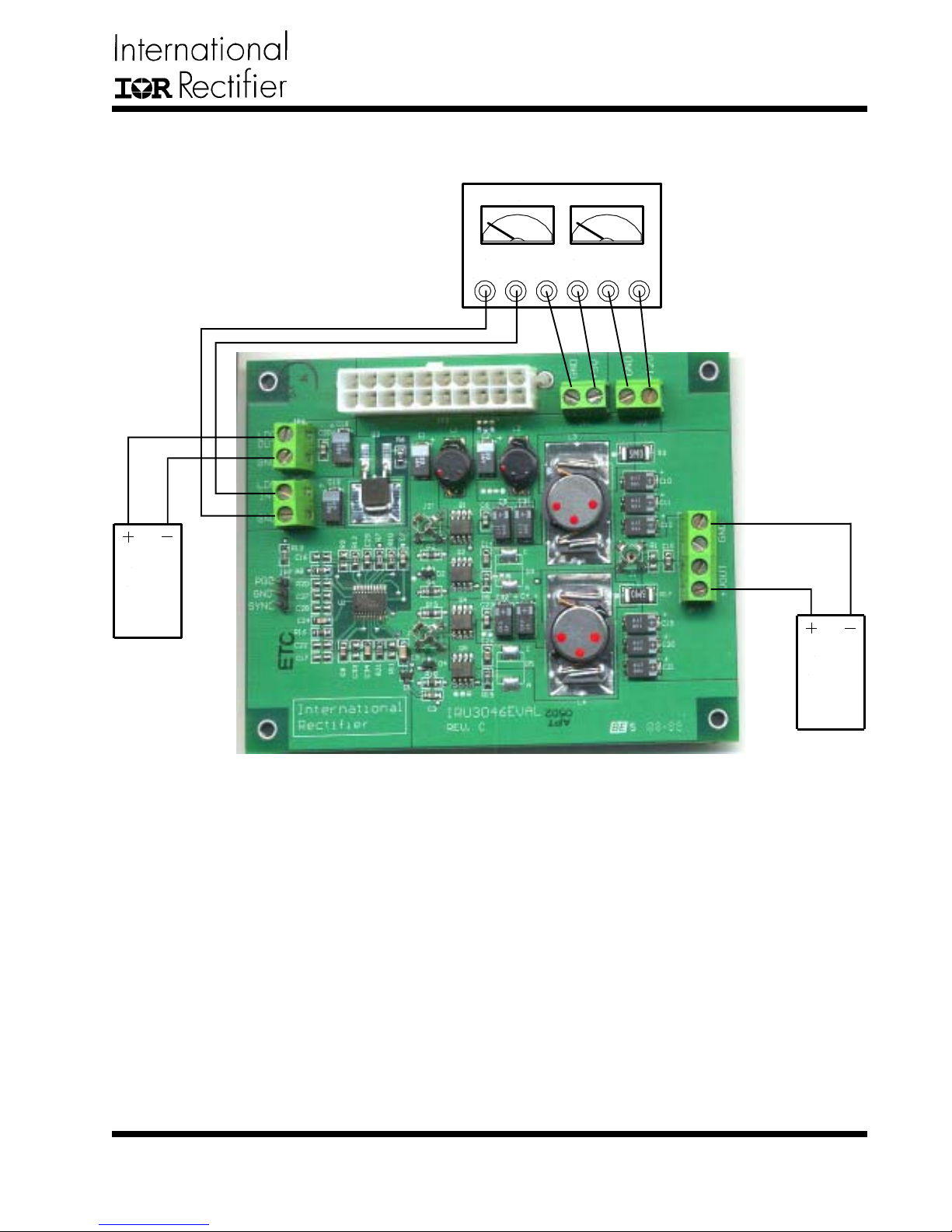
CONNECTION DIAGRAM
IRDC3046
Power Supply
Load
0 - 2A
6A Supply
Gnd +3.3V Gnd +5V Gnd +12V
6A Supply
Load
0 - 16A
Figure 1 - Connection diagram of evaluation-board for IRU3046.
Rev. 1.0
05/22/02
www.irf.com
2
Page 3
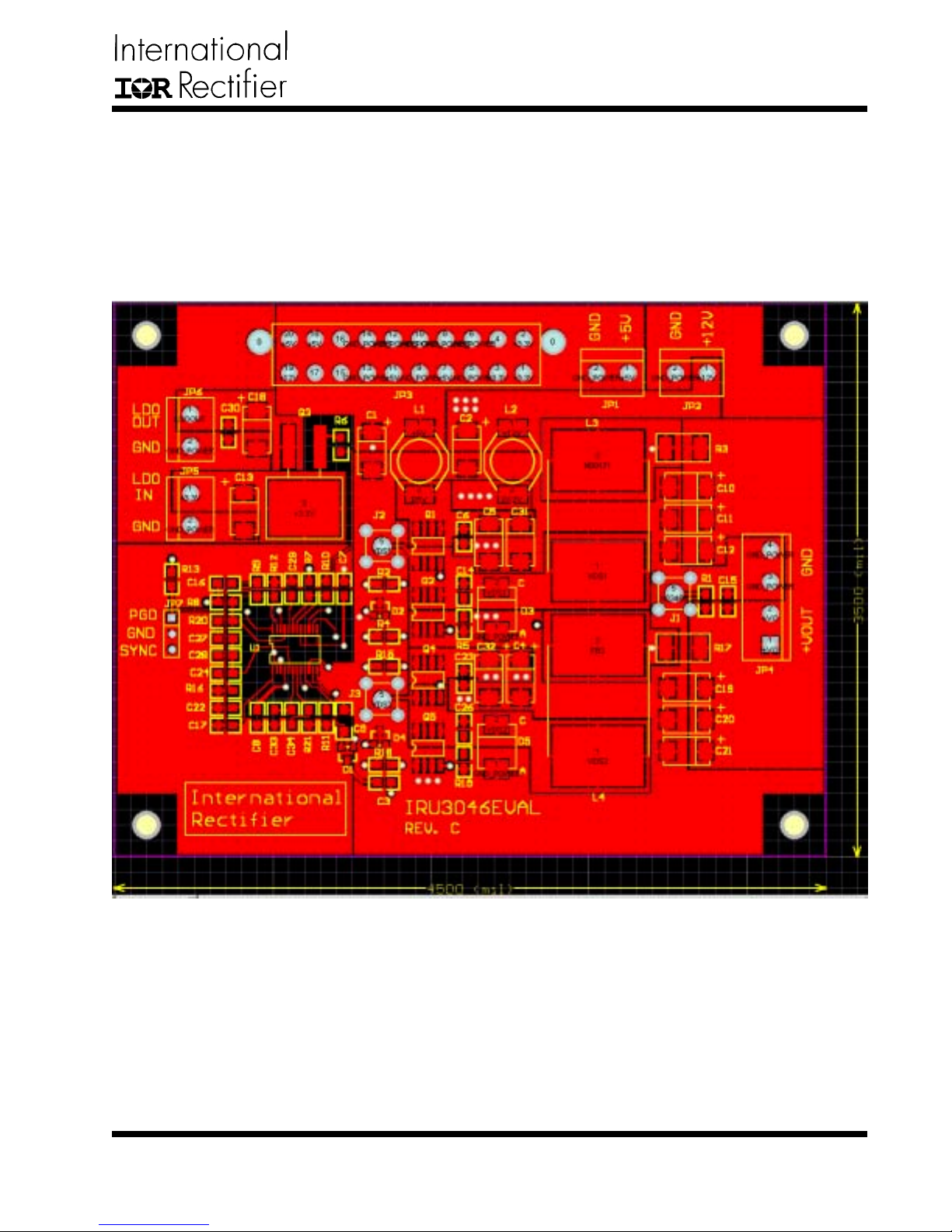
LAYOUT
The top side (component) layer for IRU3046 Eval board
is shown in Figure 2. The input capacitors are all located
close to the MOSFETs. All the decoupling capacitors,
charge pump capacitor and feedback components are
located close to IC. The two current sense resistor located close to inductors and they are located symmetri-
IRDC3046
cal to the output. The feedback resistors are tied to the
output voltage at the point of regulation.
The PCB is 4-layers board, one layer is dedicated to
Power GND and the analog GND is kept separated from
the PGND and it is connected at a single point.
Figure 2 - T op layer of evaluation-board for IRU3046.
Rev. 1.0
05/22/02
www.irf.com
3
Page 4
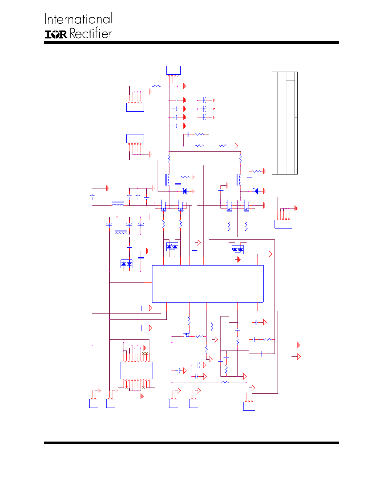
SCHEMATIC
U
D
33uF,16V,Tantalum
+
C1
5V
+5V
IRDC3046
JP4
TB41234
+VO
R1
0Ohm
12345
TP
J1
12345
J2
C31
330uF, 6.3V, PosCap
C5
330uF, 6.3V, PosCap
+
+
L1
1uH
C2
+
47uF,16V, PosCap
33uF, 16V, Tantalum
L2
1uH
D1
BAT54S
1
12V
1
+12V
+3.3V
JP3
2
C6
C4
+
+
C32
C3 0.1uF
32
C9 1uF ,25V
C8
C7
1uF
7
5
9
3
13
15
11
PG
+5V
+5V
3.3V
3.3V
GND
GND
GND
3.3V
-12V
GND
ON
GND
GND
GND
4
-5V
6
8
10
12
14
16
C12
C11
C10
TP
47uF, 16V, Posc ap
1uF
18
150uF, 6.3V, 40mOhm, PosC ap
R3
5mO hm s, 1W , 1%
VDS1
L3 2.2uH
Q1
1uF
5
IRF7460
6
3
D5V
7
2
8
1
4
R2
2.15Ohm
3 1
HDrv1
D2
BAT54A
15
VcH2
9
HDrv1
VcH1
16
VcL
13
Vcc4VccLD O17VssN S33
U1
19
+12V
+5Vsb+5V
+5V
20
22
Vc3
ATX CONN EC TOR
GN
C15
1uF
+
+
+
C16
OPEN
+
C21
+
C20
+
C19
R9
R8
150uF,6.3V, 40mOhm , PosCap
OPEN
200Ohm,1%
R12
1.00k, 1%
11
IRU3046EV AL
R17
5mOhm, 1W , 1%
R19
R5
4.7Ohm
C14 470pF
D3
OPEN
1 2
Q2
5
IRF7457
6
3
7
2
8
1
4
D12V
R4 2.15Ohm
2
Fb1
LDrv 1
C17 OPEN
12
1
14
Vref
PGnd
LDrv 1
Fb2
3
Vp22Fb121Fb2
L4 3.3uH
C23 1uF
5
6
3
7
2
8
1
4
Q4
IRF7460
VDS2
R15
2.15Ohm
D4
BAT54A
HDrv2
3 1
10
HDrv2
4.7Ohm
C26 470pF
D5
OPEN
1 2
5
6
3
7
2
8
1
4
Q5
IRF7457
R18
2.15 Ohm
2
LDrv 2
24
11
Gnd
LDrv 2
IRU3046CF
Vout3
C13
+
Q3
IRLR2703
32
47uF, Tantalum
Fb319Rt
18
R6
1
LDOout
7
Rt
Fb3
10 Ohm
R7
1.00k, 1%
R10
1.00k,1%
47uF, Tantalum
C18
+
1uF
C30
R11 OPEN
C33 OPEN
Comp1
C24
C22 OPEN
R16
R13
15k
Comp15Comp26PGood23SS
Comp2
C34
R21
2200pF
29.4K
SY NC
8
20
SS
PGoodPGood
0.1uF
C29
6800pF
C27
OPEN
R20
16.5K
C28
OPEN
IRU3046EV AL
Title
Size Document Number Rev
Date: Sheet of
12345
J3
OPEN
TP
SY NC
1
2
GND
2
JP2
TB2
GND
+12V
1
JP1
TB2
+5V
Figure 3 - Schematic of evaluation-board for IRU3046.
Rev. 1.0
05/22/02
1
2
1
GND
2
JP6
TB2
OUT
GND
JP7
123
PGD
GND
TB3
SYNC
4
ATXON-
JP5
TB2
LDOINLDO
www.irf.com
Page 5
IRDC3046
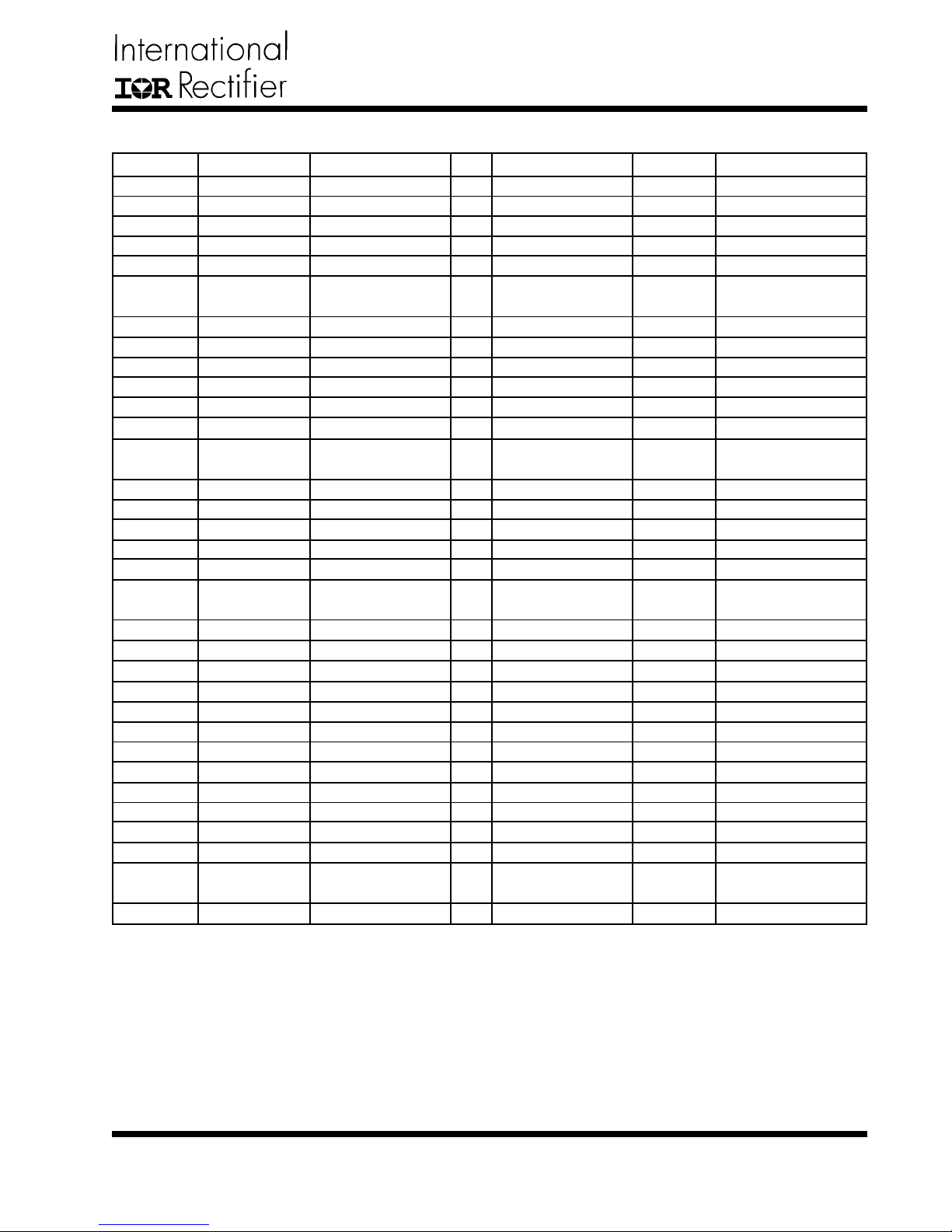
BILL OF MA TERIAL
Ref Desig Description Value Qty Part# Manuf Web site (www.)
Q1,Q4
Q2,Q5
Q3
U1
D1
D2,D4
L1,L2
L3
L4
C1,C2
C4,C32
C5,C31
C10,11,12,
19,20,21
C3,C29
C9
C24
C34
C14,C26
C6,7,8,
15,23,30
C13,C18
R2,4,15,18
R16
R21
R5,R19
R8
R7,10,12
R3,R17
R13
R6
R9,1 1,20
R1
C16,17,22,
27,28,33
D3,D5
MOSFET
MOSFET
MOSFET
Controller
Diode
Diode *
Inductor
Inductor
Inductor
Cap, T antalum
Cap, Poscap
Cap, Poscap
Cap, Poscap
Cap, Ceramic
Cap, Ceramic
Cap, Ceramic
Cap, Ceramic
Cap, Ceramic
Cap, Ceramic
Cap, T antalum
Resistor
Resistor
Resistor
Resistor
Resistor
Resistor
Resistor
Resistor
Resistor
Resistor
Resistor
Capacitor
Diode
20V , 10mV, 12A
20V , 7mV, 15A
30V , 0.045V, 23A
Synchronous PWM
Fast Switching
Fast Switching
1mH, 6.8A
2.2mH, 12A
3.3mH, 10A
33mF, 16V
47mF, 16V
330mF, 6.3V
150mF, 6.3V, 40mV
0.1mF, Y5V, 25V
1mF , X7R, 25V
2200pF , X7R, 50V
6800pF , X7R, 50V
470pF , X7R, 50V
1mF, Y5V, 16V
47mF, 10V
2.15V
29.4K
16.5K
4.7V
200, 1%
1K, 1%
5mV, 1W, 1%
15K
10V
Open
Short, 0V
Open
Open
2
IRF7460
2
IRF7457
1
IRLR2703
1
IRU3046
1
BA T54S
2
BA T54A
or 1N4148
2
D03316P-102
1
D05022P-222HC
1
D05022P-332HC
2
ECS-T1CD336R
2
16TPB47M
2
6TPB330M
6
6TPC150M
2
ECJ-2VF1E104Z
1
ECJ-3YB1E105K
1
ECJ-2VB1H222K
1
ECJ-2VB1H682K
2
ECJ-2VC1H471J
6
ECJ-2VF1C105Z
2
ECS-T1AD476R
4
1
1
2
1
3
2
ERJ-M1WSF5MOU
1
1
3
1
6
2
IR
IR
IR
IR
IR
IR
Any
Coilcraft
Coilcraft
Coilcraft
Panasonic
Sanyo
Sanyo
Sanyo
Panasonic
Panasonic
Panasonic
Panasonic
Panasonic
Panasonic
Panasonic
Panasonic
irf.com
coilcraft.com
maco.panasonic.co.jp
sanyo.com/industrial
maco.panasonic.co.jp
* Use these diodes for source/sink applications when the inductor current goes negative and for the fast load
transient from full output load to no load.
Rev. 1.0
05/22/02
www.irf.com
5
Page 6
TEST DA T A
IRDC3046
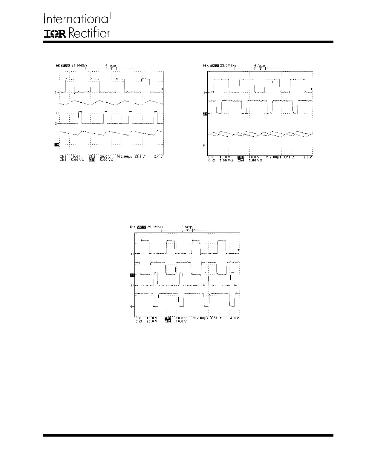
Figure 4 -
Ch1: Gate signal for control FET (master, pin-15).
Ch2: Gate signal for control FET (slave, pin-10).
Ch3: Inductor current for master channel (L3).
Ch4: Inductor current for slave channel (L4).
VMASTER=5V , VSLAVE=12V , IOUT=10A
Figure 6 -
Ch1: Gate signal for control FET (master, pin-15).
Ch2: Gate signal for sync FET (master, pin-14).
Ch3: Gate signal for control FET (slave, pin-10).
Ch4: Gate signal for sync FET (slave, pin-1 1).
Figure 5 -
Ch1: Gate signal for sync FET (master, pin-14).
Ch2: Gate signal for sync FET (slave, pin-1 1).
Ch3: Inductor current for master channel (L3).
Ch4: Inductor current for slave channel (L4).
VMASTER=5V , VSLAVE=12V , IOUT=10A
Rev. 1.0
05/22/02
www.irf.com
6
Page 7
TEST DA T A
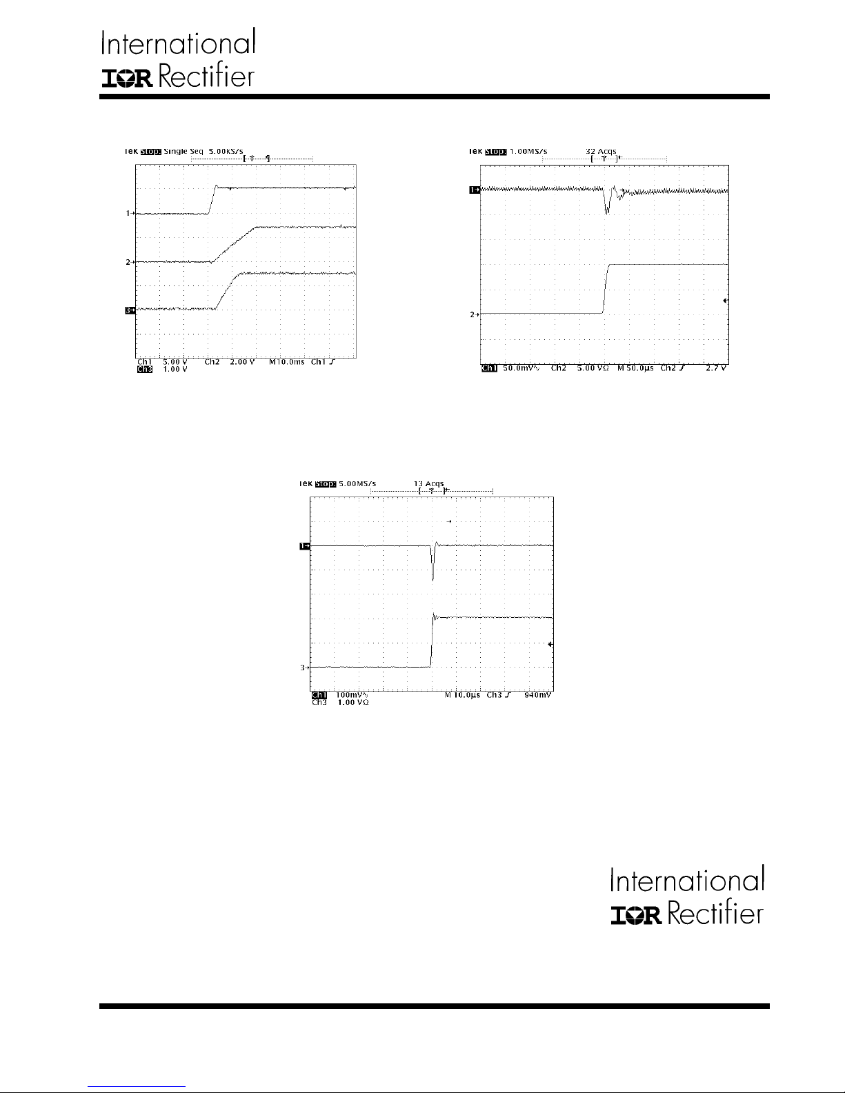
VIN=5V
IRDC3046
Vss
VOUT
0A
10A
Figure 7 - Start-up @ IOUT = 10A. Figure 8 - Transient response @ IOUT = 0 to 10A.
2A
Rev. 1.0
05/22/02
0A
Figure 9 - Transient response for
LDO @ IOUT = 0 to 2A.
IR WORLD HEADQUARTERS: 233 Kansas St., El Segundo, California 90245, USA Tel: (310) 252-7105
TAC Fax: (310) 252-7903
Visit us at www.irf.com for sales contact information
Data and specifications subject to change without notice. 7/25/2002
www.irf.com
7
 Loading...