

Datasheet IRU1050-33CT, IRU1050-33CP, IRU1050-33CM, IRU1050-33CD Datasheet (International Rectifier)
Page 1

IRU1050-33
1
Rev. 1.2
06/29/01
5A LOW DROPOUT POSITIVE
FIXED 3.3V REGULATOR
TYPICAL APPLICATION
DESCRIPTION
The IRU1050-33 is a low dropout three-terminal fixed 3.3V
output regulator with minimum of 5A output current capability. This product is specifically designed to provide
well regulated supply for low voltage IC applications requiring 3.3V output. The IRU1050-33 is guaranteed to
have <1.3V dropout at full load current making it ideal to
provide well regulated output with supply voltage as low
as 4.6V input.
Tj (°C) 3-PIN PLASTIC 3-PIN PLASTIC 2-PIN PLASTIC 2-PIN PLASTIC
T0-220 (T) TO-263 (M) Ultra Thin-Pak (P) TO-252 (D-Pak)
0 To 150 IRU1050-33CT IRU1050-33CM IRU1050-33CP IRU1050-33CD
Figure 1 - Typical application of IRU1050-33
Data Sheet No. PD94127
5V
3.3V / 5A
C1
330uF
C2
330uF
IRU1050-33
1
2
3
Vout
Gnd
Vin
PACKAGE ORDER INFORMATION
Guaranteed < 1.3V Dropout at Full Load Current
Fast Transient Response
1% Voltage Reference Initial Accuracy
Output Current Limiting
Built-In Thermal Shutdown
FEATURES
APPLICATIONS
Standard 3.3V Chip Set and Logic Applications
Page 2

IRU1050-33
2
Rev. 1.2
06/29/01
ABSOLUTE MAXIMUM RATINGS
Input Voltage (Vin) .................................................... 7V
Power Dissipation ..................................................... Internally Limited
Storage Temperature Range ...................................... -65°C To 150°C
Operating Junction Temperature Range ..................... 0°C To 150°C
PACKAGE INFORMATION
3-PIN PLASTIC TO-220 (T) 3-PIN PLASTIC TO-263 (M) 2-PIN PLASTIC ULTRA THIN-PAK (P) 2-PIN PLASTIC TO-252 (D-Pak)
θJT=2.7°C/W θJA=60°C/W θJA=35°C/W for 1" Square pad θJA=70°C/W for 1" Square pad θJA=70°C/W for 0.5" Sq pad
PARAMETER SYM TEST CONDITION MIN TYP MAX UNITS
Output Voltage Vo Io=10mA,Tj=25!C,Vin=5V 3.267 3.300 3.333 V
Io=10mA, Vin=5V 3.234 3.300 3.366
Line Regulation Io=10mA, 4.7V<Vin<7V 0.2 %
Load Regulation (Note 1) Vin=5V, Vadj=0, 10mA<Io<5A 0.4 %
Dropout Voltage (Note 2) ∆Vo Note 2, Io=5A 1.1 1.3 V
Current Limit Vin=5V, dVo=100mV 5.1 A
Minimum Load Current Vin=5V 5 10 mA
(Note 3)
Thermal Regulation 30ms Pulse, Vin-Vo=3V, Io=5A 0.01 0.02 %/W
Ripple Rejection f=120Hz, Co=25µF Tantalum,
Io=2.5A, Vin-Vo=3V 60 70 dB
Adjust Pin Current Change Io=10mA,Vin-Vo=1.5V, Tj=25!C 0.2 5 µA
Temperature Stability Vin=5V, Vadj=0V, Io=10mA 0.5 %
Long Term Stability Tj=125!C, 1000Hrs 0.3 1 %
RMS Output Noise Tj=25!C, 10Hz<f<10KHz 0.003 %Vo
ELECTRICAL SPECIFICATIONS
Unless otherwise specified, these specifications apply over Cin=1µF, Cout=10µF, and Tj=0 to 150!C.
Typical values refer to Tj=25!C.
Note 1: Low duty cycle pulse testing with Kelvin connections is required in order to maintain accurate data.
Note 2: Dropout voltage is defined as the minimum differential voltage between Vin and Vout required to maintain regulation at Vout. It is measured when the output
voltage drops 1% below its nominal value.
Note 3: Minimum load current is defined as the minimum current required at the output in order for the output voltage to maintain regulation. Typically the resistor
dividers are selected such that it automatically maintains this current.
Gnd
Vin
Ta b i s
Vou t
FRONT VIEW
1
3
Gnd
Vin
Tab is
Vout
FRONT VIEW
1
3
Gnd
Vou t
Vin
Ta b i s
Vou t
FRONT VIEW
1
2
3
Tab is
Vout
Gnd
Vin
Vout
1
2
3
FRONT VIEW
Page 3
IRU1050-33
3
Rev. 1.2
06/29/01
APPLICATION INFORMATION
Stability
The IRU1050-33 requires the use of an output capacitor as part of the frequency compensation in order to make the
regulator stable. Typical designs for microprocessor applications use standard electrolytic capacitors with a typical
ESR in the range of 50 to 100mΩ and an output capacitance of 500 to 1000µF. Fortunately as the capacitance
increases, the ESR decreases resulting in a fixed RC time constant. The IRU1050-33 takes advantage of this
phenomena in making the overall regulator loop stable. For most applications a minimum of 100µF aluminum
electrolytic capacitor such as Sanyo MVGX series, Panasonic FA series as well as the Nichicon PL series insures
both stability and good transient response.
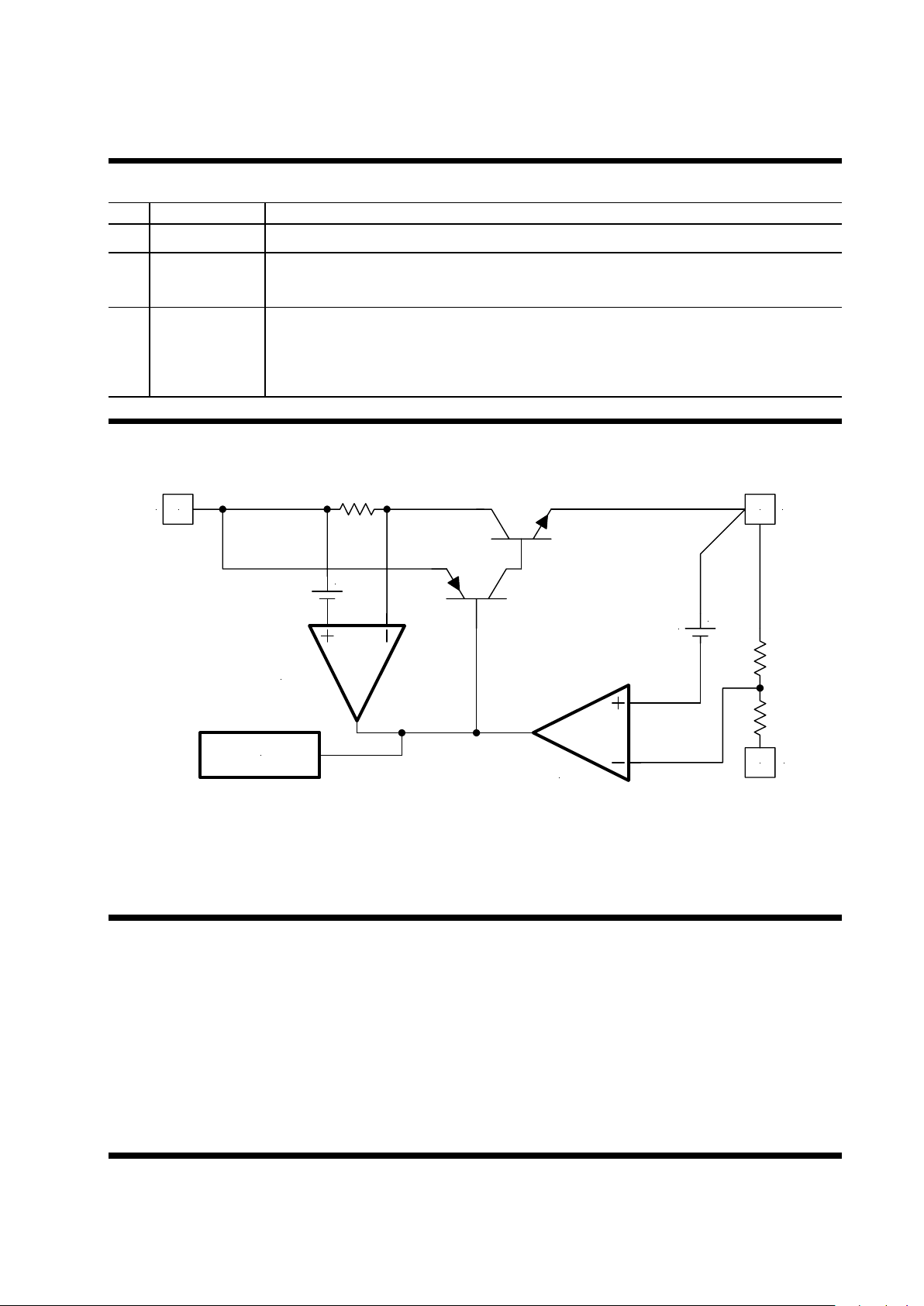
Vin 3
1050-33blk1-1.0
1 Gnd
2 Vout
THERMAL
SHUTDOWN
CURRENT
LIMIT
1.25V
+
+
PIN # PIN SYMBOL PIN DESCRIPTION
PIN DESCRIPTIONS
This pin must be connected to ground plane using a low inductance short connection.
The output of the regulator. A minimum of 10µF capacitor must be connected from this pin
to ground to insure stability.
The input pin of the regulator. Typically a large storage capacitor is connected from this
pin to ground to insure that the input voltage does not sag below the minimum dropout
voltage during the load transient response. This pin must always be 1.3V higher than Vout
in order for the device to regulate properly.
BLOCK DIAGRAM
Figure 1 - Simplified block diagram of the IRU1050-33
1
2
3
Gnd
Vout
Vin
Page 4
IRU1050-33
4
Rev. 1.2
06/29/01
Notes
IR WORLD HEADQUARTERS : 233 Kansas St., El Segundo, California 90245, USA Tel: (310) 252-7105
TAC Fax: (310) 252-7903
Visit us at www.irf.com for sales contact information.
Data and specifications subject to change without notice. 02/01
 Loading...