

Page 1

Data Sheet No. PD94119
IRU1010
1A LOW DROPOUT POSITIVE
ADJUSTABLE REGULATOR
FEATURES
Guaranteed < 1.3V Dropout at Full Load Current
Fast Transient Response
1% Voltage Reference Initial Accuracy
Built-In Thermal Shutdown
Available in SOT-223, D-Pak, Ultra Thin-Pak and
8-Pin SOIC Surface-Mount Packages
APPLICATIONS
VGA & Sound Card Applications
Low Voltage High Speed Termination Applications
Standard 3.3V Chip Set and Logic Applications
TYPICAL APPLICATION
D1
5V
C1
10uF
Vin
3
DESCRIPTION
The IRU1010 is a low dropout, three-terminal adjustable
regulator with minimum of 1A output current capability.
This product is specifically designed to provide well regulated supply for low voltage IC applications such as high
speed bus termination and low current 3.3V logic supply. The IRU1010 is also well suited for other applications such as VGA and sound cards. The IRU1010 is
guaranteed to have <1.3V dropout at full load current
making it ideal to provide well regulated outputs of 2.5V
to 3.6V with 4.75V to 7V input supply.
IRU1010
Vout
2
R1
121
Adj
1
R2
1010app1-1.4
Figure 1 - Typical application of IRU1010 in a 5V to 2.85V SCSI termination regulator
154
C2
22uF
PACKAGE ORDER INFORMATION
Tj (°C) 2-PIN PLASTIC 3-PIN PLASTIC 2-PIN PLASTIC 8-PIN PLASTIC
TO-252 (D-Pak) SOT-223 (Y) Ultra Thin-Pak (P) SOIC (S)
0 To 150 IRU1010CD IRU1010CY IRU1010CP IRU1010CS
2.85V / 1A
Rev. 1.4
06/29/01
1
Page 2

IRU1010
ABSOLUTE MAXIMUM RATINGS
Input Voltage (Vin) .................................................... 7V
Power Dissipation ..................................................... Internally Limited
Storage Temperature Range ...................................... -65°C To 150°C
Operating Junction Temperature Range ..................... 0°C To 150°C
PACKAGE INFORMATION
2-PIN PLASTIC TO-252 (D-Pak) 3-PIN PLASTIC SO-223 (Y) 2-PIN ULTRA THIN-PAK (P) 8-PIN PLASTIC SOIC (S)
Tab is
Vou t
FRONT VIEW
Vout
TOP VIEW
3
Vin
2
Vout
1
Adj
3
Vin
Tab is
1
Adj
Tab is
Vou t
FRONT VIEW
3
Vin
1
Adj
Vin
NC
NC
TOP VIEW
1
2
3
4
8
Vout
7
Vout
6
Vout
5
VoutAdj
θJA=70!C/W for 0.5" Sq pad θJA=90!C/W for 0.4" Sq pad θJA=70!C/W for 0.5" Sq pad θJA=55!C/W for 1" Sq pad
ELECTRICAL SPECIFICATIONS
Unless otherwise specified, these specifications apply over Cin=1µF, Cout=10µF, and Tj=0 to 150!C.
Typical values refer to Tj=25!C.
PARAMETER SYM TEST CONDITION MIN TYP MAX UNITS
Reference Voltage Vref Io=10mA, Tj=25!C, (Vin-Vo)=1.5V 1.238 1.250 1.262 V
Io=10mA, (Vin-Vo)=1.5V 1.225 1.250 1.275
Line Regulation Io=10mA, 1.3V<(Vin-Vo)<7V 0.2 %
Load Regulation (Note 1) Vin=3.3V, Vadj=0, 10mA<Io<1A 0.4 %
Dropout Voltage (Note 2) ∆Vo Note 2 , Io=1A 1.1 1.3 V
Current Limit Vin=3.3V, dVo=100mV 1.1 A
Minimum Load Current Vin=3.3V, Vadj=0V 5 10 mA
(Note 3)
Thermal Regulation 30ms Pulse, Vin-Vo=3V, Io=1A 0.01 0.02 %/W
Ripple Rejection f=120Hz, Co=25µF Tantalum,
Io=0.5A, Vin-Vo=3V 60 70 dB
Adjust Pin Current Iadj Io=10mA, Vin-Vo=1.5V, Tj=25!C,
Io=10mA, Vin-Vo=1.5V 55 120 µA
Adjust Pin Current Change Io=10mA, Vin-Vo=1.5V, Tj=25!C 0.2 5 µA
Temperature Stability Vin=3.3V, Vadj=0V, Io=10mA 0.5 %
Long Term Stability Tj=125!C, 1000Hrs 0.3 1 %
RMS Output Noise Tj=25!C, 10Hz<f<10KHz 0.003 %Vo
Note 1: Low duty cycle pulse testing with Kelvin connections is required in order to maintain accurate data.
Note 2: Dropout voltage is defined as the minimum differential voltage between Vin and Vout required to maintain regulation at Vout. It is measured when the output
voltage drops 1% below its nominal value.
2
Note 3: Minimum load current is defined as the mini-
mum current required at the output in order for the output voltage to maintain regulation. Typically, the resistor
dividers are selected such that it automatically maintains this current.
Rev. 1.4
06/29/01
Page 3
PIN DESCRIPTIONS
PIN # PIN SYMBOL PIN DESCRIPTION
1
Adj
A resistor divider from this pin to the Vout pin and ground sets the output voltage.
IRU1010
2
3
Vout
Vin
The output of the regulator. A minimum of 10µF capacitor must be connected from this pin
to ground to insure stability.
The input pin of the regulator. Typically a large storage capacitor is connected from this
pin to ground to insure that the input voltage does not sag below the minimum dropout
voltage during the load transient response. This pin must always be 1.3V higher than Vout
in order for the device to regulate properly.
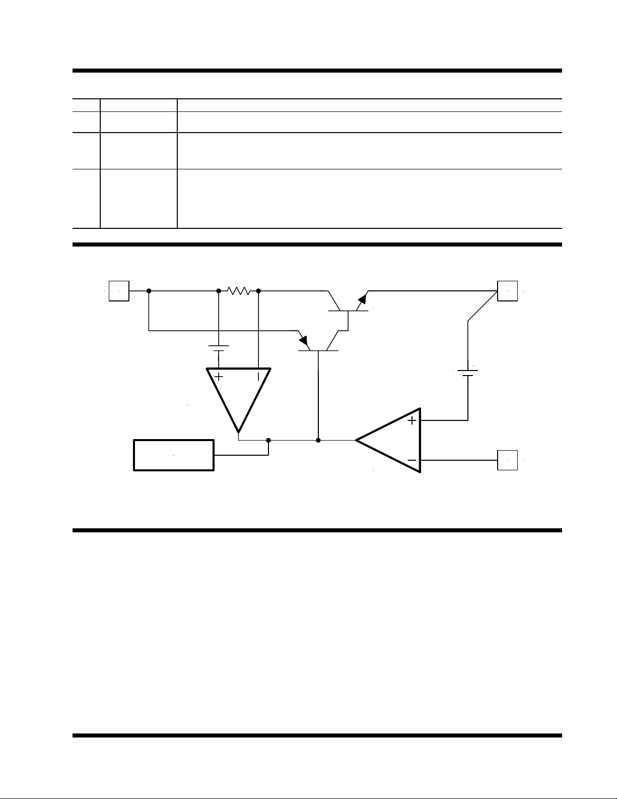
BLOCK DIAGRAM
Vin 3
CURRENT
LIMIT
2 Vout
+
1.25V
+
THERMAL
SHUTDOWN
Figure 2 - Simplified block diagram of the IRU1010
APPLICATION INFORMATION
Introduction
The IRU1010 adjustable Low Dropout (LDO) regulator is
a three-terminal device which can easily be programmed
with the addition of two external resistors to any voltages within the range of 1.25 to 5.5V. This regulator,
unlike the first generation of the three-terminal regulators such as LM117 that required 3V differential between
the input and the regulated output, only needs 1.3V differential to maintain output regulation. This is a key requirement for today’s low voltage IC applications that
typically need 3.3V supply and are often generated from
the 5V supply. Other applications such as high speed
1010blk1-1.0
memory termination need to switch the load current from
zero to full load in tens of nanoseconds at their pins,
which translates to an approximately 300 to 500ns current step at the regulator. In addition, the output voltage
tolerances are sometimes tight and they include the transient response as part of the specification.
The IRU1010 is specifically designed to meet the fast
current transient needs as well as providing an accurate
initial voltage, reducing the overall system cost with the
need for fewer output capacitors.
1 Adj
Rev. 1.4
06/29/01
3
Page 4
IRU1010
Output Voltage Setting
The IRU1010 can be programmed to any voltages in the
range of 1.25V to 5.5V with the addition of R1 and R2
external resistors according to the following formula:
R2
V
OUT = VREF ×
oo
o1 +
oo
Where:
REF = 1.25V Typically
V
IADJ = 50µA Typically
R1 and R2 as shown in figure 3:
Vin
IRU1010
pp
p + IADJ × R2
pp
R1
Vou tVin
Adj
Vre f
Vout
R1
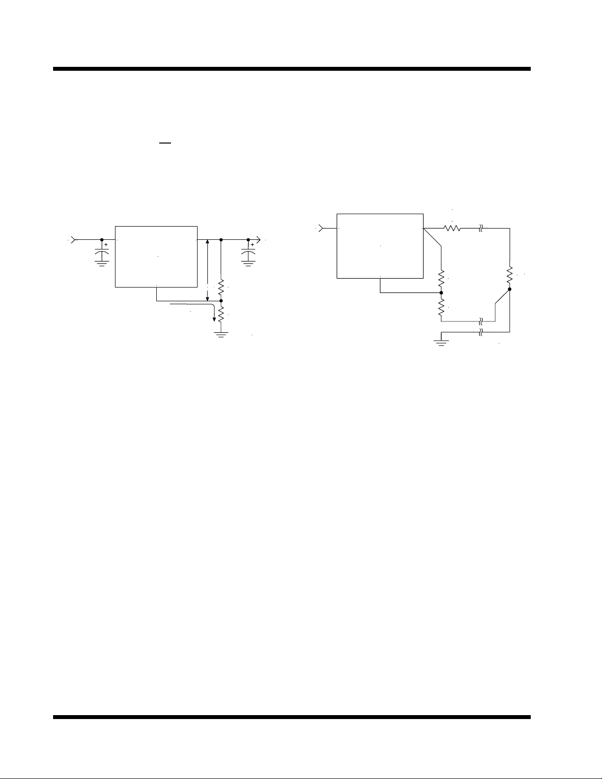
regulator and not to the load. In fact, if R1 is connected
to the load side, the effective resistance between the
regulator and the load is gained up by the factor of (1+R2/
R1), or the effective resistance will be, Rp(eff)=Rp*(1+R2/
R1). It is important to note that for high current applications, this can represent a significant percentage of the
overall load regulation and one must keep the path from
the regulator to the load as short as possible to minimize this effect.
PARASITIC LI NE
RESISTANCE
Rp
Vin
VoutVin
IRU1010
Adj
R1
R
L
IAdj = 50uA
R2
1010app2-1.0
Figure 3 - Typical application of the IRU1010
for programming the output voltage
The IRU1010 keeps a constant 1.25V between the output pin and the adjust pin. By placing a resistor R1 across
these two pins a constant current flows through R1, adding to the I
current and into the R2 resistor producing
adj
a voltage equal to the (1.25/R1)*R2 + Iadj*R2 which will
be added to the 1.25V to set the output voltage. This is
summarized in the above equation. Since the minimum
load current requirement of the IRU1010 is 10mA, R1 is
typically selected to be 121Ω resistor so that it automatically satisfies the minimum current requirement.
Notice that since Iadj is typically in the range of 50µA it
only adds a small error to the output voltage and should
only be considered when a very precise output voltage
setting is required. For example, in a typical 3.3V application where R1=121Ω and R2=200Ω the error due to
Iadj is only 0.3% of the nominal set point.
Load Regulation
Since the IRU1010 is only a three-terminal device, it is
not possible to provide true remote sensing of the output
voltage at the load. Figure 4 shows that the best load
regulation is achieved when the bottom side of R2 is
connected to the load and the top side of R1 resistor is
connected directly to the case or the Vout pin of the
R2
1010app3-1.0
Figure 4 - Schematic showing connection
for best load regulation
Stability
The IRU1010 requires the use of an output capacitor as
part of the frequency compensation in order to make the
regulator stable. Typical designs for microprocessor applications use standard electrolytic capacitors with a
typical ESR in the range of 50 to 100mΩ and an output
capacitance of 500 to 1000µF. Fortunately as the capacitance increases, the ESR decreases resulting in a
fixed RC time constant. The IRU1010 takes advantage
of this phenomena in making the overall regulator loop
stable. For most applications a minimum of 100µF aluminum electrolytic capacitor such as Sanyo MVGX series, Panasonic FA series as well as the Nichicon PL
series insures both stability and good transient response.
Thermal Design
The IRU1010 incorporates an internal thermal shutdown
that protects the device when the junction temperature
exceeds the maximum allowable junction temperature.
Although this device can operate with junction temperatures in the range of 150!C, it is recommended that the
selected heat sink be chosen such that during maximum continuous load operation the junction temperature is kept below this number. The example below for
a SCSI terminator application shows the steps in sellect-
4
Rev. 1.4
06/29/01
Page 5
IRU1010
ing the proper regulator in a surface-mount package.
(See IRU1015 for non-surface-mount packages)
Assuming the following specifications:
VIN = 5V
VF = 0.5V
Vo = 2.85V
IOUT(MAX) = 0.8A
TA = 35!C
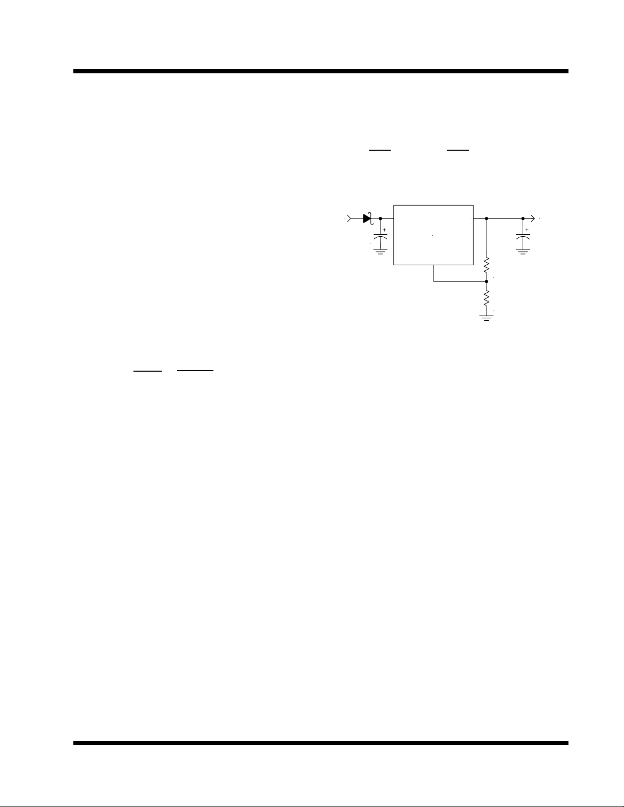
Where: VF is the forward voltage drop of the D1diode as
shown in Figure 5.
The steps for selecting the right package with proper
board area for heatsinking to keep the junction temperature below 135!C is given as:
1) Calculate the maximum power dissipation using:
PD = IOUT × (VIN - VF - VOUT)
PD = 0.8 × (5 - 0.5 - 2.85) = 1.32W
2) Calculate the maximum
θJA(MAX) = = = 75.6!C/W
TJ - TA
PD
θJA allowed for our example:
135 - 35
1.32
3) Select a package from the datasheet with lower θJA
than the one calculated in the previous step.
Selecting TO-252 (D-Pak) with at least 0.5" square
of 0.062" FR4 board using 1 oz. copper has 70°C/W
which is lower than the calculated number.
To set the output DC voltage, we need to select R1 and
R2:
4) Assuming R1 = 121Ω, 1%
R2 =
VOUT
oo
o -1
oo
VREF
pp
p× R1 =
pp
2.85
oo
o - 1
oo
1.25
pp
p× 121 = 154.8Ω
pp
Select R2 = 154Ω, 1%
D1
5V
C1
10uF
IRU1010
Adj
Vou tVin
R1
121
1%
R2
154
1%
C2
22uF
1010app4-1.3
2.85V
Figure 5 - Final Schematic for half of the
GTL+ termination regulator
Layout Consideration
The output capacitors must be located as close to the
Vout terminal of the device as possible. It is recommended to use a section of a layer of the PC board as a
plane to connect the Vout pin to the output capacitors to
prevent any high frequency oscillation that may result
due to excessive trace inductance.
Rev. 1.4
06/29/01
5
Page 6

IRU1010
Notes
6
IR WORLD HEADQUARTERS : 233 Kansas St., El Segundo, California 90245, USA Tel: (310) 252-7105
TAC Fax: (310) 252-7903
Visit us at www.irf.com for sales contact information.
Data and specifications subject to change without notice. 02/01
Rev. 1.4
06/29/01
 Loading...