

Page 1
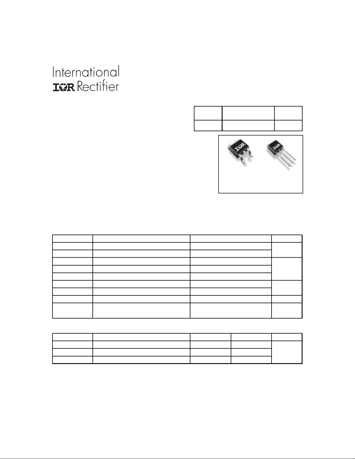
Applications
High Frequency Synchronous Buck
Converters for Computer Processor Power
High Frequency Isolated DC-DC
Converters with Synchronous Rectification
for Telecom and Industrial Use
Benefits
Very Low RDS(on) at 4.5V V
Ultra-Low Gate Impedance
Fully Characterized Avalanche Voltage
GS
and Current
Absolute Maximum Ratings
Parameter Units
V
DS
V
GS
@ TC = 25°C
I
D
@ TC = 100°C
I
D
I
DM
P
@TC = 25°C
D
@TC = 100°C
P
D
T
J
T
STG
Drain-to-Source Voltage V
Gate-to-Source Voltage
Continuous Drain Current, V
Continuous Drain Current, V
Pulsed Drain Current
Maximum Power Dissipation
Maximum Power Dissipation
Linear Derating Factor W/°C
Operating Junction and °C
Storage Temperature Range
@ 10V
GS
@ 10V
GS
V
DSS
30V
PD - 94538
IRLR7821
IRLU7821
HEXFET® Power MOSFET
R
DS(on)
D-Pak
IRLR7821
Max.
30
± 20
65
47
260
75
1.5
0.50
-55 to + 175
10m
max
Ω
Qg
10nC
I-Pak
IRLU7821
A
W
Thermal Resistance
Parameter Typ. Max. Units
R
θ
JC
R
θ
JA
R
θ
JA
Junct ion-to-Case ––– 2.0
Junct ion-to-Ambient (PCB Mount)
Junct ion-to-Ambient ––– 110
––– 50 °C/W
Notes through are on page 11
www.irf.com 1
08/27/02
Page 2
IRLR/U7821
/
gy
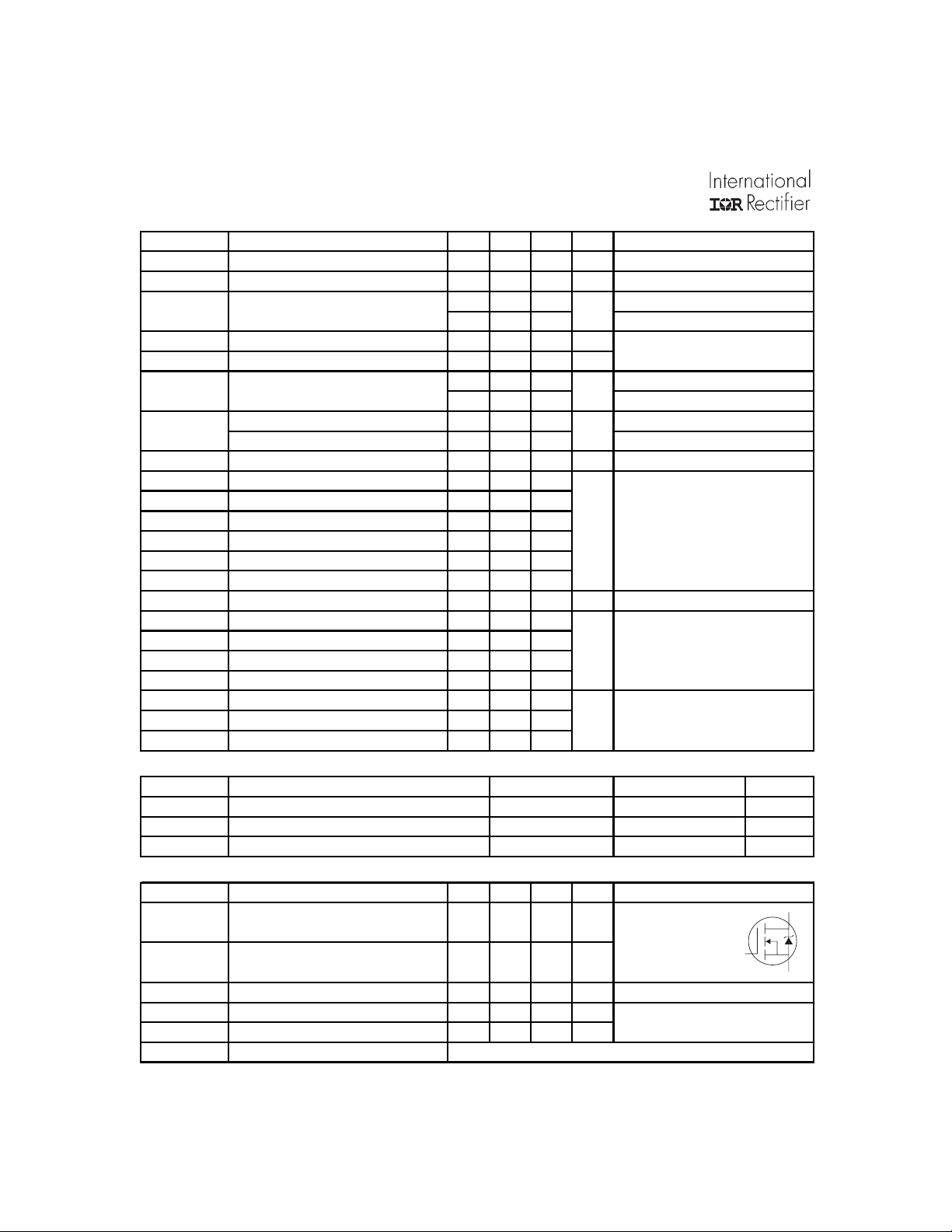
Static @ TJ = 25°C (unless otherwise specified)
Parameter Min. Typ. Max. Units
BV
DSS
∆Β
V
DSS
R
DS(on)
V
GS(th)
∆
V
GS(th)
I
DSS
I
GSS
gfs Forward Transconductance 46 ––– ––– S
Q
g
Q
gs1
Q
gs2
Q
gd
Q
godr
Q
sw
Q
oss
t
d(on)
t
r
t
d(off)
t
f
C
iss
C
oss
C
rss
Drain-to-Source Breakdown Voltage 30 ––– ––– V
∆
T
Breakdown Voltage Temp. Coefficient ––– 23 ––– mV/°C
J
Static Drain-to-Source On-Resistance ––– 7.5 10
––– 9.5 12.5
Gate Threshold Voltage 1.0 ––– ––– V
Gate Threshold Voltage Coefficient ––– -5.3 ––– mV/°C
Drain-to-Source Leakage Current ––– ––– 1.0 µA
––– ––– 150
Gate-to-Source Forward Leakage ––– ––– 100 nA
Gate-to-Source Reverse Leakage ––– ––– -100
Total Gate Charge ––– 10 14
Pre-Vth Gate-to-Source Charge ––– 2.0 –––
Post-Vth Gate-to-Source Charge ––– 1.2 ––– nC
Gate-to-Drain Charge ––– 2.5 –––
Gate Charge Overdrive ––– 4.3 ––– See Fig. 16
Switch Charge (Q
gs2
+ Qgd)
––– 3.7 –––
Output Charge ––– 8.5 ––– nC
Turn-On Delay Time ––– 11 –––
Rise Time ––– 4.2 –––
Turn-Off Delay Time ––– 10 ––– ns
Fall Time ––– 3.2 –––
Input Capacitance ––– 1030 –––
Output Capacitance ––– 360 ––– pF
Reverse Transfer Capacitance ––– 120 –––
VGS = 0V, ID = 250µA
Reference to 25°C, I
mΩ
= 10V, ID = 15A
V
GS
V
= 4.5V, ID = 12A
GS
V
= VGS, ID = 250µA
DS
V
= 24V, VGS = 0V
DS
V
= 24V, VGS = 0V, TJ = 125°C
DS
V
= 20V
GS
V
= -20V
GS
= 15V, ID = 12A
V
DS
= 16V
V
DS
= 4.5V
V
GS
I
= 12A
D
V
= 16V, VGS = 0V
DS
= 15V, VGS = 4.5V
V
DD
I
= 12A
D
Clamped Inductive Load
V
= 0V
GS
V
= 15V
DS
ƒ = 1.0MHz
Conditions
= 1mA
D
Avalanche Characteristics
Parameter Units
E
AS
I
AR
E
AR
Single Pulse Avalanche Ener
Avalanche Current
Repetitive Avalanche Energy
Typ.
–––
–––
–––
Max.
230
12
7.5
mJ
A
mJ
Diode Characteristics
Parameter Min. Typ. Max. Units
I
S
Continuous Source Current ––– –––
(Body Diode) A
I
SM
V
SD
t
rr
Q
rr
t
on
Pulsed Source Current ––– ––– 260
(Body Diode)
Diode Forward Voltage ––– ––– 1.0 V
Reverse Recovery Time ––– 26 38 ns
Reverse Recovery Charge ––– 15 23 nC
Forward Turn-On Time
Intrinsic turn-on time is negligible (turn-on is dominated by LS+LD)
65
MOSFET symbol
showing the
integral reverse
p-n junction diode.
= 25°C, IS = 12A, VGS = 0V
T
J
= 25°C, IF = 12A, VDD = 15V
T
J
di/dt = 100A/µs
Conditions
G
2 www.irf.com
D
S
Page 3
IRLR/U7821
10000
)
A
(
t
n
e
r
r
u
C
e
c
r
u
o
S
o
t
n
i
a
r
D
,
D
I
1000
100
10
1
TOP 10V
BOTTOM 2.5V
VGS
4.5V
3.7V
3.5V
3.3V
3.0V
2.7V
2.5V
20µs PULSE WIDTH
0.1
0.1 1 10 100
Tj = 25°C
VDS, Drain-to-Source Voltage (V)
1000
1000
TOP 10V
)
A
(
t
n
e
r
100
r
u
C
e
c
r
u
o
S
o
t
n
i
a
r
D
,
D
I
BOTTOM 2.5V
10
VGS
4.5V
3.7V
3.5V
3.3V
3.0V
2.7V
2.5V
20µs PULSE WIDTH
Tj = 175°C
1
0.1 1 10 100
VDS, Drain-to-Source Voltage (V)
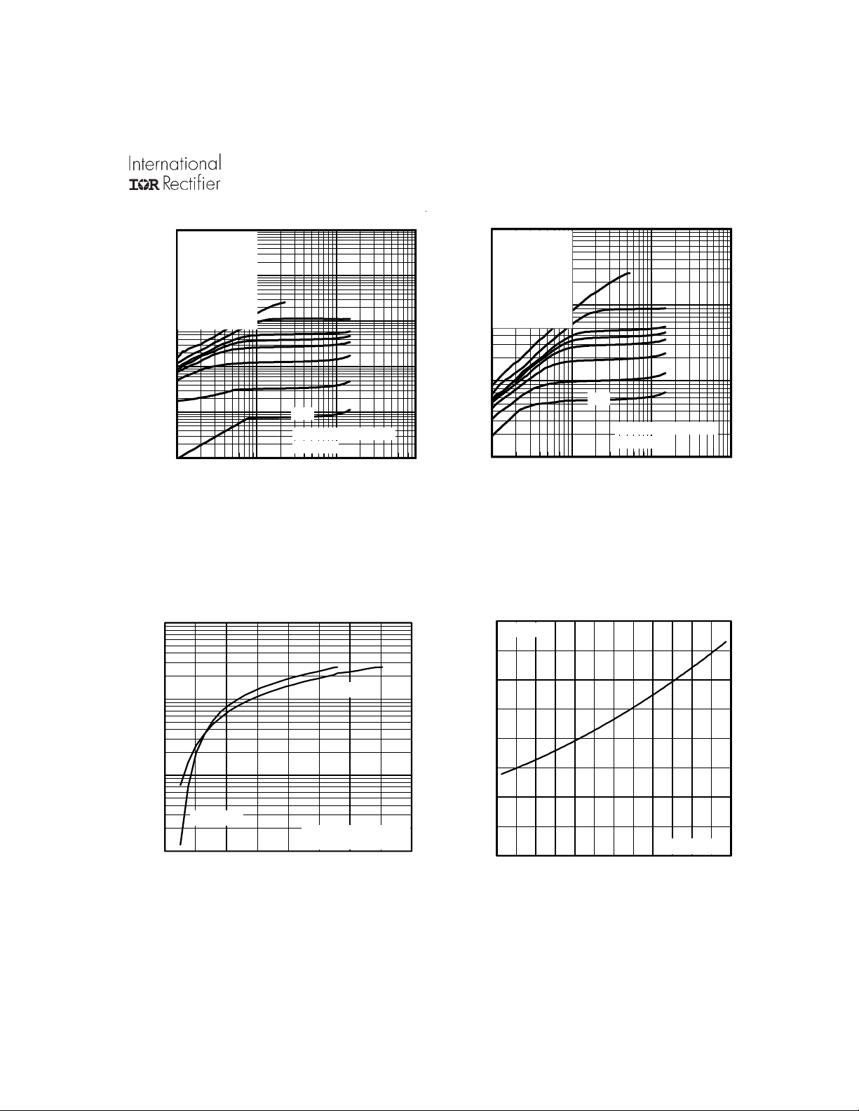
Fig 2. Typical Output CharacteristicsFig 1. Typical Output Characteristics
2.0
65A
I =
D
T = 175 C
100
10
D
I , Drain-to-Source Current (A)
1
2.0 4.0 6.0 8.0 10. 0
°
T = 25 C
J
V , Gate-to-Source Voltage (V)
GS
J
V = 15V
DS
20µs PULSE WID TH
Fig 3. Typical Transfer Characteristics
°
1.5
1.0
(Normalized)
0.5
DS(on)
R , Drain-to-Source On Resistance
0.0
-60 -40 -20 0 20 40 60 80 100 120 140 160 180
TJ, Junction Temperature (°C)
Fig 4. Normalized On-Resistance
V =
GS
10V
Vs. Temperature
www.irf.com 3
Page 4
IRLR/U7821
10000
)
F
1000
p
(
e
c
n
a
t
i
c
a
p
a
C
,
100
C
10
1 10 100
V
= 0V, f = 1 MHZ
GS
C
= C
+ Cgd, C
iss
gs
C
= C
rss
gd
C
= C
ds
+ C
oss
C
C
C
gd
iss
oss
rss
SHORTED
ds
VDS, Drain-to-Source Voltage (V)
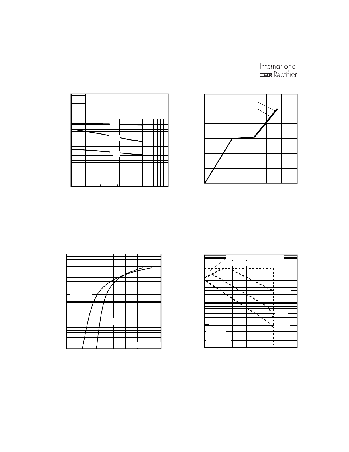
Fig 5. Typical Capacitance Vs.
Drain-to-Source Voltage
1000
100
°
T = 175 C
J
10
°
T = 25 C
1
SD
I , Reverse Drain Current (A)
0.1
0.0 0. 5 1.0 1.5 2.0
V ,Source- to-Dr ain Voltage (V)
SD
J
V = 0 V
6
ID= 12A
)
V
5
(
e
g
a
t
l
4
o
V
e
c
r
u
3
o
S
o
t
e
t
2
a
G
,
S
1
G
V
VDS= 24V
VDS= 16V
0
024681012
Q
Total Gate Charge (nC)
G
Fig 6. Typical Gate Charge Vs.
Gate-to-Source Voltage
1000
)
A
(
t
100
n
e
r
r
u
C
e
c
r
u
10
o
S
o
t
n
i
a
r
1
D
,
Tc = 25°C
D
I
Tj = 175°C
Single Pulse
GS
0.1
1 10 100
OPERATION IN THIS AREA
LIMITED BY RDS(on)
100µsec
1msec
10msec
VDS, Drain-to-Source Voltage (V)
Fig 7. Typical Source-Drain Diode
Fig 8. Maximum Safe Operating Area
Forward Voltage
4 www.irf.com
Page 5
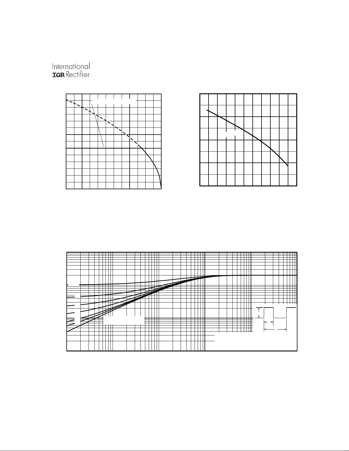
IRLR/U7821
70
LIMITED BY PACKAGE
60
50
40
30
D
20
I , Drain Current (A)
10
0
25 50 75 100 125 150 175
T , Case Temperature ( C)
C
°
Fig 9. Maximum Drain Current Vs.
Case Temperature
10
2.5
)
V
(
e
g
2.0
a
t
l
o
V
d
l
o
h
s
1.5
e
r
h
t
e
t
a
G
)
h
1.0
t
(
S
G
V
0.5
-75 -50 -25 0 25 50 75 100 125 150 175 200
ID = 250µA
TJ , Temperature ( °C )
Fig 10. Threshold Voltage Vs. Temperature
thJC
D = 0.50
1
0.20
0.10
0.05
0.1
0.02
0.01
SINGLE PULSE
(THERMAL RESPONSE)
Thermal Response (Z )
Not es:
1. Duty factor D = t / t
2. Peak T = P x Z + T
0.01
0.00001 0.0001 0.001 0.01 0.1 1
t , Rectangular Pulse Duration (sec)
1
J DM thJC C
1 2
P
DM
t
1
t
2
Fig 11. Maximum Effective Transient Thermal Impedance, Junction-to-Case
www.irf.com 5
Page 6
IRLR/U7821
A
+
-
15V
V
DS
R
G
20V
V
GS
L
D.U.T
I
AS
Ω
0.01
t
p
DRIVER
+
V
DD
-
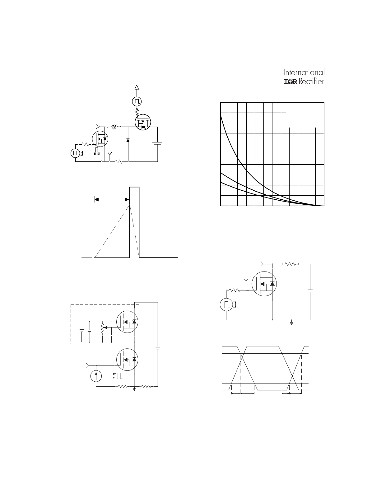
Fig 12a. Unclamped Inductive Test Circuit
V
(BR)DSS
t
p
I
AS
Fig 12b. Unclamped Inductive Waveforms
Current Regulator
Same Type as D.U.T.
50KΩ
12V
.2µF
.3µF
D.U.T.
+
V
DS
-
1000
TOP
800
600
400
200
AS
E , Single Pulse Avalanche Energy (mJ)
0
25 50 75 100 125 150 175
Starti ng Tj , Junction Temperature ( C)
BOTTO M
°
Fig 12c. Maximum Avalanche Energy
Vs. Drain Current
R
V
DS
V
GS
R
G
V
GS
Pulse Width ≤ 1 µs
Duty Factor ≤ 0.1 %
D
D.U.T.
Fig 14a. Switching Time Test Circuit
V
DS
90%
I
D
4.9A
8.5A
12A
V
DD
V
GS
3mA
10%
I
G
Current Sampling Resistors
I
D
Fig 13. Gate Charge Test Circuit
V
GS
t
d(on)tr
t
d(off)tf
Fig 14b. Switching Time Waveforms
6 www.irf.com
Page 7
IRLR/U7821
+
-
Reverse
Recovery
Current
Driver Gate Drive
D.U.T. ISDWaveform
D.U.T. VDSWaveform
Inductor Curent
* V
GS
D.U.T
+
-
R
G
+
Circuit Layout Considerations
• Low Stray Inductance
• Ground Plane
-
• Low Leakage Inductance
Current Transformer
-
• dv/dt controlled by R
• Driver same type as D.U.T.
• ISD controlled by Duty Factor "D"
• D.U.T. - Device Under Test
G
+
V
DD
Re-Applied
Voltage
Period
P.W.
Body Diode Forward
Current
di/dt
Diode Recovery
dv/dt
Body Diode Forward Drop
Ripple ≤ 5%
= 5V for Logic Level Devices
D =
P. W .
Period
VGS=10V
V
DD
I
SD
*
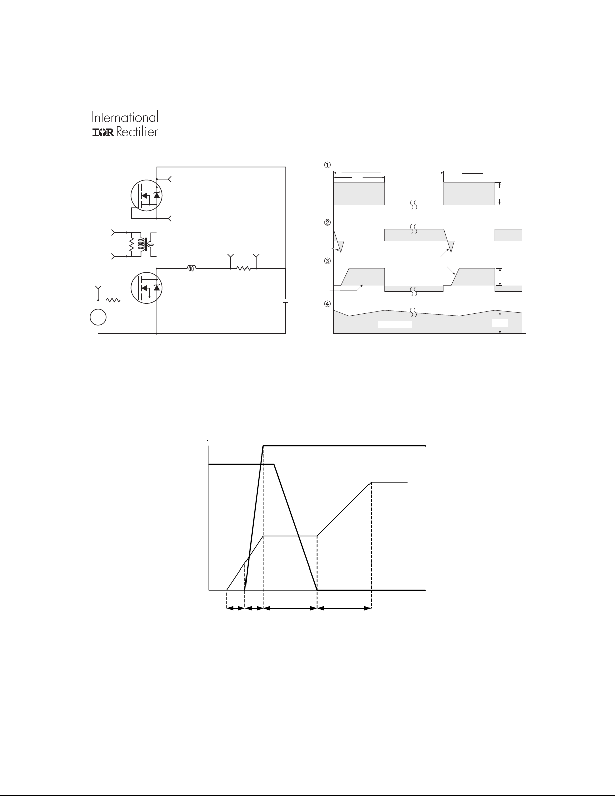
Fig 15. Peak Diode Recovery dv/dt Test Circuit for N-Channel
HEXFET® Power MOSFETs
Id
Vds
Vgs
Vgs(th)
Qgs1
Qgs2 Qgd Qgodr
Fig 16. Gate Charge Waveform
www.irf.com 7
Page 8
IRLR/U7821
)
Power MOSFET Selection for Non-Isolated DC/DC Converters
Control FET
Special attention has been given to the power losses
in the switching elements of the circuit - Q1 and Q2.
Power losses in the high side switch Q1, also called
the Control FET, are impacted by the R
MOSFET, but these conduction losses are only about
one half of the total losses.
Power losses in the control switch Q1 are given
by;
P
= P
loss
This can be expanded and approximated by;
P
loss
conduction
= I
()
rms
+ I ×
+ Q
()
g
Q
+
This simplified loss equation includes the terms Q
and Q
charge that is included in all MOSFET data sheets.
The importance of splitting this gate-source charge
into two sub elements, Q
Fig 16.
the gate driver between the time that the threshold
voltage has been reached and the time the drain current rises to I
gins to change. Minimizing Q
reducing switching losses in Q1.
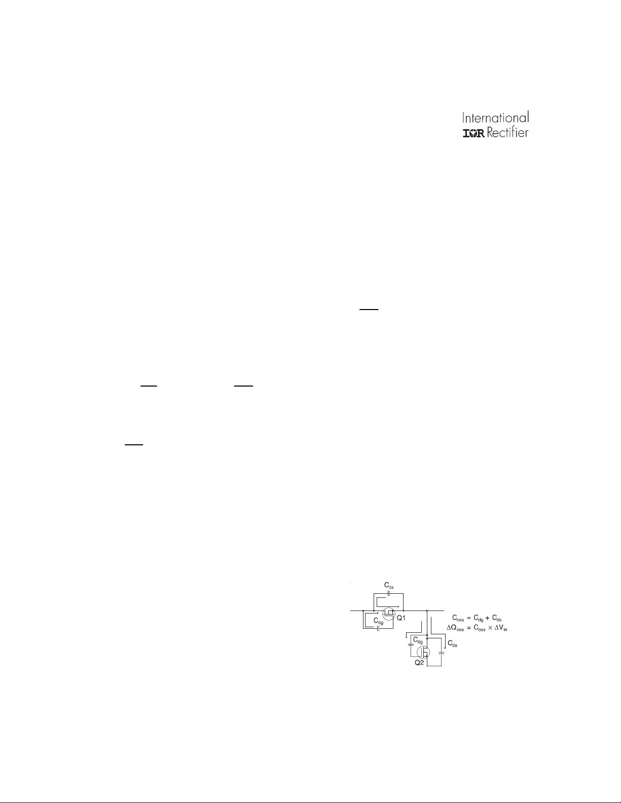
put capacitance of the MOSFET during every switching cycle. Figure A shows how Q
parallel combination of the voltage dependant (nonlinear) capacitance’s Cds and Cdg when multiplied by
the power supply input buss voltage.
which are new to Power MOSFET data sheets.
oss
Q
is a sub element of traditional gate-source
gs2
Q
indicates the charge that must be supplied by
gs2
Q
is the charge that must be supplied to the out-
oss
2
Q
× R
gd
i
g
+ P
ds(on)
× Vin× f
switching
+ P
+ I ×
drive
+ P
Q
i
gs2
g
× Vg× f
oss
×Vin× f
2
dmax
and Q
gs1
at which time the drain voltage be-
, can be seen from
gs2
is a critical factor in
gs2
is formed by the
oss
of the
ds(on)
output
× Vin× f
Synchronous FET
The power loss equation for Q2 is approximated
by;
P
= P
loss
conduction
P
= I
loss
+ Qg× Vg× f
+
rms
()
Q
*dissipated primarily in Q1.
For the synchronous MOSFET Q2, R
portant characteristic; however, once again the im-
portance of gate charge must not be overlooked since
it impacts three critical areas. Under light load the
MOSFET must still be turned on and off by the control IC so the gate drive losses become much more
significant. Secondly, the output charge Q
verse recovery charge Qrr both generate losses that
are transfered to Q1 and increase the dissipation in
that device. Thirdly, gate charge will impact the
MOSFETs’ susceptibility to Cdv/dt turn on.
gs2
The drain of Q2 is connected to the switching node
of the converter and therefore sees transitions between ground and Vin. As Q1 turns on and off there is
a rate of change of drain voltage dV/dt which is capacitively coupled to the gate of Q2 and can induce
a voltage spike on the gate that is sufficient to turn
the MOSFET on, resulting in shoot-through current .
The ratio of Qgd/Q
potential for Cdv/dt turn on.
Figure A: Q
+ P
2
× R
ds(on)()
oss
× Vin× f
2
must be minimized to reduce the
gs1
Characteristic
oss
drive
+ P
*
output
+ Q
(
× Vin× f
rr
ds(on)
oss
is an im-
and re-
8 www.irf.com
Page 9
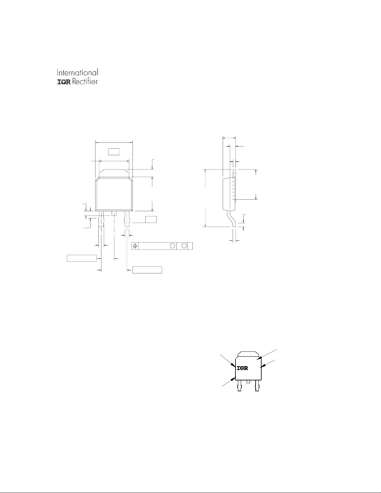
TO-252AA (D-Pak) Package Outline
I
N
T
E
R
N
A
T
I
O
N
A
L
L
O
G
O
R
E
C
T
I
F
I
E
R
3
4
1
2
I
R
F
U
1
2
0
9
1
6
A
L
O
T
C
O
D
E
A
S
S
E
M
B
L
Y
E
X
A
M
P
L
E
:
W
I
T
H
A
S
S
E
M
B
L
Y
T
H
I
S
I
S
A
N
I
R
F
R
1
2
0
Y
E
A
R
9
=
1
9
9
9
D
A
T
E
C
O
D
E
L
I
N
E
A
W
E
E
K
1
6
I
N
T
H
E
A
S
S
E
M
B
L
Y
L
I
N
E
"
A
"
A
S
S
E
M
B
L
E
D
O
N
W
W
1
6
,
1
9
9
9
L
O
T
C
O
D
E
1
2
3
4
P
A
R
T
N
U
M
B
E
R
Dimensions are shown in millimeters (inches)
IRLR/U7821
5.46 (.215 )
5.21 (.205 )
1.02 (.040)
1.64 (.025)
1.52 (.060)
1.15 (.045)
1.14 (.045)
2X
0.76 (.030)
2.28 (.090)
6.73 (.265)
6.35 (.250)
- A -
4
1 2 3
1.27 (.050 )
0.88 (.035 )
6.22 (.245)
5.97 (.235)
- B -
0.89 (.035)
3X
0.64 (.025)
0.25 (.010) M A M B
4.57 (.180)
2.38 (.094)
2.19 (.086)
10.42 (.410)
9.40 (.37 0)
NOTES:
1 DIMENSIONING & TOLERANCING PER ANSI Y14.5M, 1982.
2 CONTROLLING DIMENSION : INCH.
3 CONFORMS TO JE DEC OUTLINE TO-252AA.
4 DIMENSIONS SHOWN ARE BEFORE SOLDER DIP,
SOLD ER DIP MAX. +0. 16 (.0 06).
1.14 (.045)
0.89 (.035)
0.58 (.02 3)
0.46 (.01 8)
6.45 (.245)
5.68 (.224)
0.51 (.02 0)
MIN.
0.58 (.023)
0.46 (.018)
LEAD ASSIGNMENTS
1 - GATE
2 - DRAIN
3 - SOURCE
4 - DRAIN
TO-252AA (D-Pak) Part Marking Information
www.irf.com 9
Page 10
IRLR/U7821
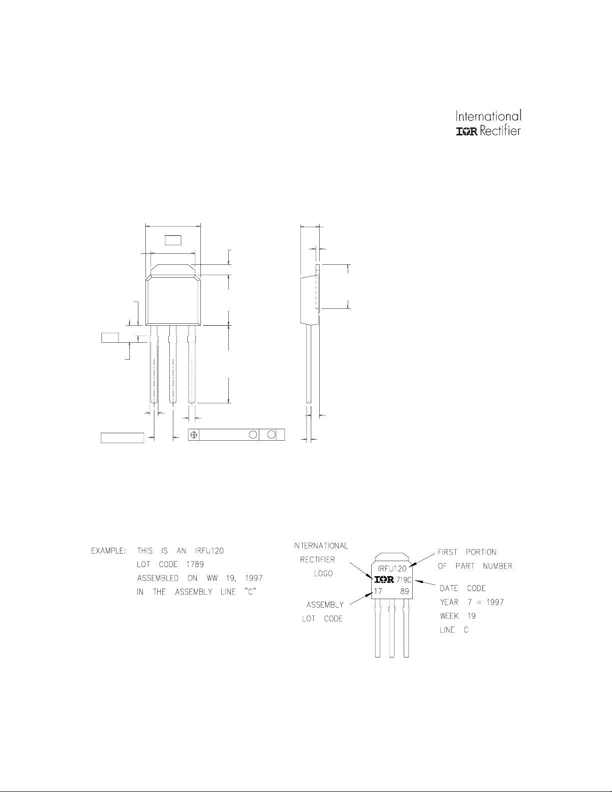
I-Pak (TO-251AA) Package Outline
Dimensions are shown in millimeters (inches)
5.46 (.215)
5.21 (.205)
1.52 (.060)
1.15 (.045)
- B -
2.28 (.090)
1.91 (.075)
1.14 (.045)
3X
0.76 (.030)
2.28 (.090)
6.73 (.265)
6.35 (.250)
- A -
4
1 2 3
3X
2X
1.27 (.050)
0.88 (.035)
6.22 (.245)
5.97 (.235)
9.65 (.380)
8.89 (.350)
0.89 (.035)
0.64 (.025)
0.25 (.010) M A M B
2.38 (.094)
2.19 (.086)
0.58 (.023)
0.46 (.018)
6.45 (.245)
5.68 (.224)
NOTES:
1 DIMENSIONING & TOLERANCING PER ANSI Y14.5M, 1982.
2 CONTROLLING DIMENSION : INCH.
3 C ONFORMS TO J EDEC OUTLINE TO-25 2AA.
4 D IMENSION S SHOW N ARE BEF ORE SOLDER DIP,
SOLDER DIP MAX. +0.16 (.006).
1.14 (.045)
0.89 (.035)
0.58 (.023)
0.46 (.018)
I-Pak (TO-251AA) Part Marking Information
LEAD ASSIGNMENTS
1 - GATE
2 - DRAIN
3 - SOURCE
4 - DRAIN
10 www.irf.com
Page 11
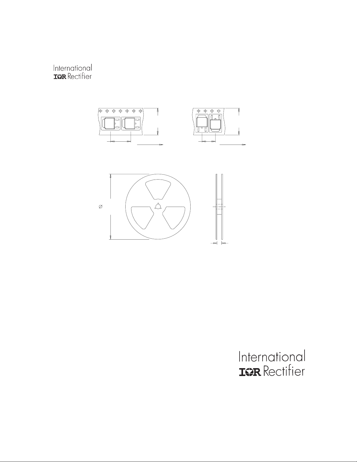
D-Pak (TO-252AA) Tape & Reel Information
Dimensions are shown in millimeters (inches)
TR
TRR
IRLR/U7821
TRL
12.1 ( .47 6 )
11.9 ( .46 9 )
NOTES :
1. CONTROLLIN G DIMENSION : MILLIMETER.
2. ALL DIMENSIONS ARE SHOWN IN MILLIMETERS ( INCHES ).
3. OUTLINE CONFORMS TO EIA-481 & EIA-541.
13 INCH
NOTES :
1. OUTLINE CONFORMS TO EIA-481.
FEED DIRECT ION
Notes:
Repetitive rating; pulse width limited by
max. junction temperature.
Starting T
RG = 25Ω, I
= 25°C, L = 3.2mH
J
= 12A.
AS
Pulse width ≤ 400µs; duty cycle ≤ 2%.
16.3 ( .641 )
15.7 ( .619 )
16.3 ( .641 )
15.7 ( .619 )
8.1 ( .318 )
7.9 ( .312 )
16 mm
FEED DIRECTION
Calculated continuous current based on maximum allowable
junction temperature. Package limitation current is 30A.
When mounted on 1" square PCB (FR-4 or G-10 Material).
For recommended footprint and soldering techniques refer to
application note #AN-994.
Data and specifications subject to change without notice.
This product has been designed and qualified for the Industrial market.
Qualification Standards can be found on IR’s Web site.
IR WORLD HEADQUARTERS: 233 Kansas St., El Segundo, California 90245, USA Tel: (310) 252-7105
TAC Fax: (310) 252-7903
Visit us at www.irf.com for sales contact information.08/02
www.irf.com 11
 Loading...