

Page 1
Bay Linear
Bay Linear
Bay LinearBay Linear
Linear Excellenc e
POWER MOSFET
Description
The Bay Linear MOSFET’s p r ovide the designers with t he best
combination of fast switching, ruggedized device design, low
0n-resistance and low cost-effectiveness.
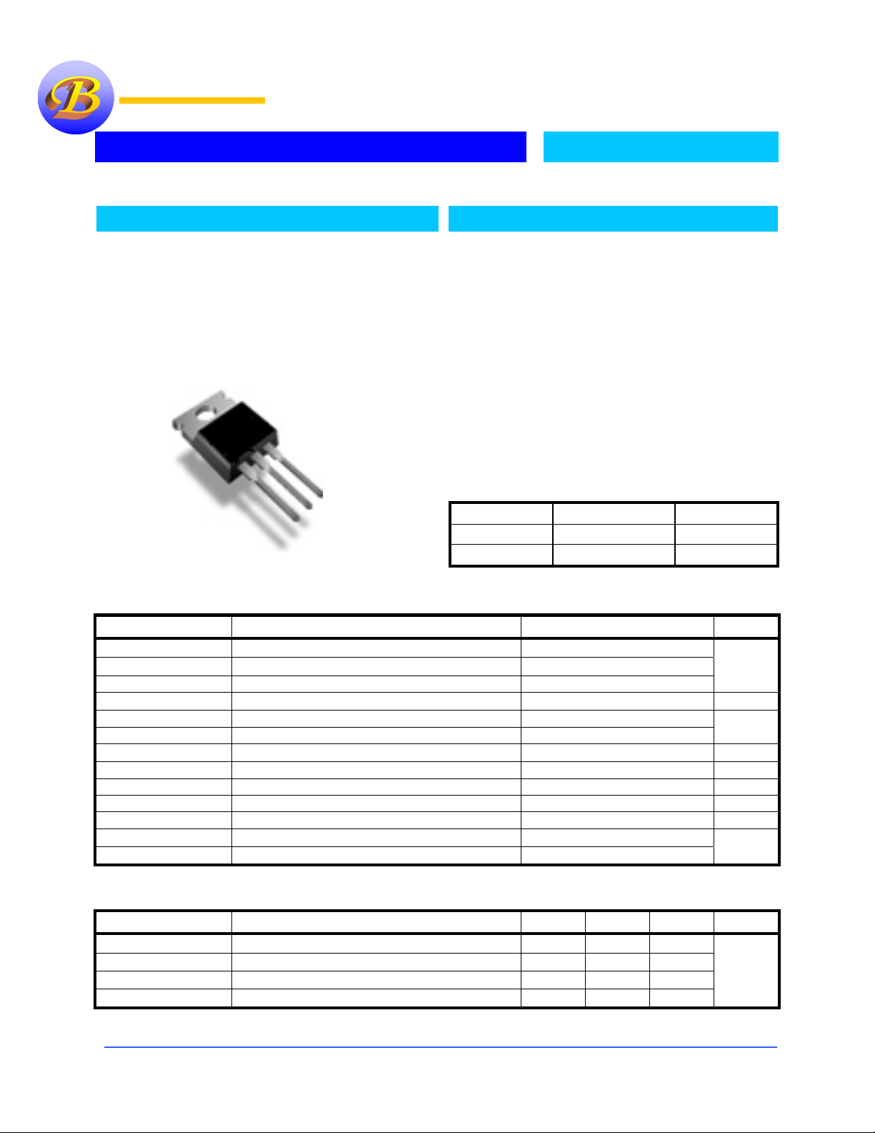
The TO-220 is offered in a 3-pin is universally preferred for all
commercial-industrial applications at power dissipation level
to approximately to 50 watts. Also, available in a D
mount power package with a power dissipation up to 2 Watts
2
surface
Advance Information
IRF830
Features
Dynamic dv/dt Rating
•
Repetitive Avalanche Rated
•
Fast Switching
•
Ease of Paralleling
•
Simple Drive Requirements
•
V
= 500V
DSS
R
DS (ON)
I
= 4.5A
D
= 1.5 Ω
Ordering Information
Device Package Temp.
IRL830T TO-220
IRL830S TO-263 ( D2 )
0 to 150°C
0 to 150°C
Absolute Maximum Rating
ID@ TC =25°°°°C
ID@ TC =100°°°°C
IDM
PD @ TC =25°°°°C
V
GS
E
AS
I
AR
E
AR
dv/dt
TJ, T
STG
Continuous Drain Current, V
Continuous Drain Current, V
Pulsed Drain Current (1) 18
Power Dissipation 74
Linear Derating Factor 0.59
Linear Derating Factor ( PCB Mount, D
Gate-to- Source Voltage
Single Pulse Avalanche Energy (2) 280
Avalanche Current (1) 4.5
Repetitive Avalanche Energy (1) 7.4
Peak Diode Recovery dv/dt (3) 3.5
Junction & Storage Temperature Range
Soldering Temperature, for 10 seconds 300 (1.6mm from case)
Thermal Resistance
R
JC
θθθθ
R
CS
θθθθ
R
JA
θθθθ
R
JA
θθθθ
Junction-to Case - - 1.7
Case-to-Sink, Flat, Greased Surface ( TO-220)
Junction-to Ambient ( PCB Mount, D2 )
Junction-to Ambient - - 62
Parameter Max Unit
@10V 4.5
Parameter
GS
@10V 2.9
GS
2
) (1) 0.025
±
20
−
55 to +150
Min Typ Max Units
- 0.50
40
A
W
W/°°°°C
V
mJ
A
mJ
V/ns
°°°°C
°°°°C/W
Bay Linear, Inc
2478 Armstrong Street, Livermore, CA 94550 Tel: (925) 989-7144, Fax: (925) 940-9556 www.baylinear.com
Page 2
IRF830
Electrical Characteristics (
TC = 25°°°°C unless otherwise specified)
Symbol Parameter Conditions Min Typ Max Units
V
(BR)DSS
V
(BR)DSS
∆∆∆∆T
I
D(ON)
R
DS(ON)
V
GS(TH)
g
fs
I
DSS
J
Drain-to-source Breakdown
Voltage
/
Breakdown Voltage
Temperature Coefficient
On-State Drain Current
(note 2)
Static Drain-to-Source
On-Resistance
Gate Threshold Voltage
Forward Transconductance
Drain-to-Source Leakage
Current
V
V
GS
V
V
Gate-to-Source Forward
I
GSS
Leakage
Gate-to-Source Reverse
Leakage
Q
g
Q
qs
Q
gd
t
d ( on)
T
r
t
d (off)
T
f
LD
L
S
C
iss
C
oss
C
rss
Total Gate Charge ID =3.1A - - 38
Gate-to-Source Charge V
Gate-to-Drain (“Miller”)
Charge
Turn-On Delay Time - 8.2 Rise Time - 16 Turn -Off Delay Time - 42 Fall Time
Internal Drain Inductance - 4.5
Between lead 6mm (0.25in.)
from package and center or die
Internal Source Inductance
Input Capacitance - 610 Output Capacitance - 160 Reverse Transfer Capacitance
Source-Drain Rating Characteristics
= 0V, ID = 250µA
GS
Reference to 25°C,
I
= 1mA
D
> I
D(ON)
V
=10V, ID = 2.7A
GS
x R
DS(ON)
Max
(note 4)
DS = VGS, ID =
50V, ID = 2.7A
V
DS =
250µA
V
500V, V
DS =
= 400V, V
DS
T
V
V
DS
V
= 10V (note 4) 22
GS
V
DD
I
D
R
GS
= 125°C
C
= 20V 100
GS
= -20V
G
= 400V - - 5.0
= 250V
= 3.1.1A
Ω
= 12
G
0V 25
GS =
= 0V,
RD = 79Ω (note 4)
contact
V
= 0V
GS
V
= 25V
DS
F = 1.0MHZ
500
- 0.61 -
4.5
1.5
2.0 - 4.0
2.5 - -
- 250
- -
-100
- 16 -
-
- 7.5 -
- 68 -
V
V/°°°°C
A
ΩΩΩΩ
V
S
µµµµA
nA
nC
ns
nH
pF
Symbol Parameter Conditions Min Typ Max Units
I
S
I
SM
V
SD
t
rr
Q
rr
t
on
Notes: 1. Repetitive Rating; pulse width limited by max. junction temperature.
2. V
3. I
4. Pulse with ≤ 300µs; duty cycle ≤ 2%
Continuous Source Current
(Body Diode)
Pulsed Source Current
(Body Diode) (Note 1)
Diode Forward Voltage (note 4)
Reverse Recovery Time - 320 640
Reverse Recovery Charge
Forward Turn-On Time Intrinsic turn-on time is negligible (turn-on is dominated by (LS+LD)
= 50V, starting Tj = 25 °C, L = 24 mH RG = 25Ω, I
DD
≤ 4.5A, di/dt ≤ 75A/µs, VDD ≤ V
SD
(BR)DSS
MOSFET symbol showing the
integral reverse p-n junction
diode.
=25°C, IS=2.5A,VGS=DV
T
J
T
=25°C, IF=2.1A
J
di/dt=100A/µs (Note 4)
= 4.5A
, T
j
≤ 150°C
AS
- - 4.5
- - 18
- - 1.6
- 1.0 2.0
A
V
ns
µµµµC
Bay Linear, Inc
2478 Armstrong Street, Livermore, CA 94550 Tel: (925) 989-7144, Fax: (925) 940-9556 www.baylinear.com
Page 3

-
Advance Information
computer simulations and/ or initial prototype evaluation.
These data sheets contain descriptions of products that are in development. The specifications are based on the engineering calculations,
-
Preliminary Information
subject to change upon the completion of the full characterization over the specified temperature and supply voltage ranges.
These data sheets contain minimum and maximum specifications that are based on the initial device characterizations. These limits are
The application circuit examples are only to explain the representative applications of the devices and are not intended to guarantee an y circuit
design or permit any industrial property right to other rights to execute. Bay Linear takes no responsibi lity for any problems rela ted to any
industrial property right resulting from the use of the contents shown in the data b ook. Typical parameters can and do vary in different
applications. Customer’s technical experts must validate all operating parameters including “ Typical” for each customer application.
LIFE SUPPORT AND NUCLEAR POLICY
Bay Linear products are not authorized for and should not be used within life support systems which are intended for surgical
implants into the body to support or sustain life, in aircraft, space equipment, submarine, or nuclear facility applicatio ns without
the specific written consent of Bay Linear President.
Bay Linear, Inc
2478 Armstrong Street, Livermore, CA 94550 Tel: (925) 989-7144, Fax: (925) 940-9556 www.baylinear.com
 Loading...