

Page 1
Bulletin I27130 rev. G 10/02
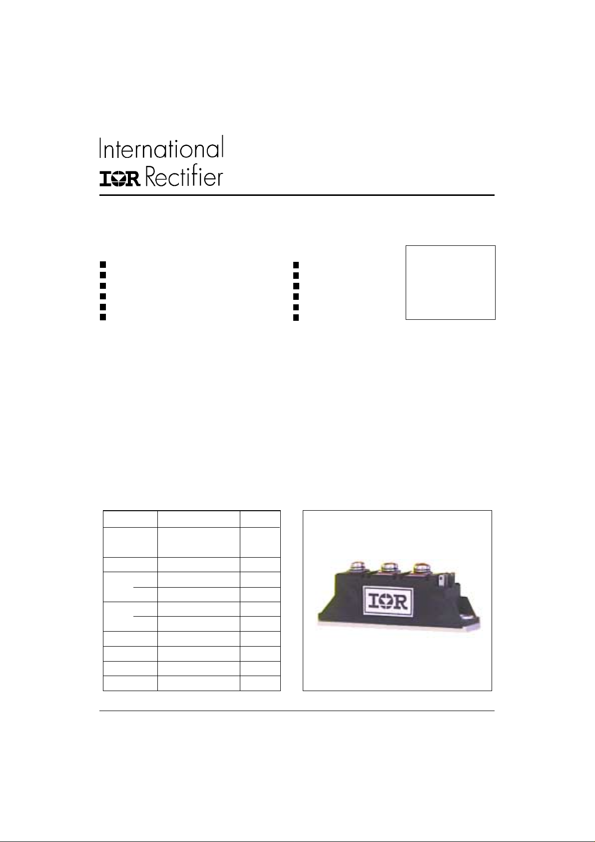
IRK.26 SERIES
THYRISTOR/ DIODE and
THYRISTOR/ THYRISTOR
Features
High Voltage
Industrial Standard Package
Thick Al metal die and double stick bonding
Thick copper baseplate
UL E78996 approved
3500V
isolating voltage
RMS
Mechanical Description
The Generation V of Add-A-pak module combine the
excellent thermal performance obtained by the usage of
Direct Bonded Copper substrate with superior
mechanical ruggedness, thanks to the insertion of a solid
Copper baseplate at the bottom side of the device.
The Cu baseplate allow an easier mounting on the
majority of heatsink with increased tolerance of surface
roughness and improve thermal spread.
The Generation V of AAP module is manufactured without
hard mold, eliminating in this way any possible direct
stress on the leads.
ADD-A-pakTM GEN V Power Modules
Benefits
Up to 1600V
Full compatible TO-240AA
High Surge capability
Easy Mounting on heatsink
Al203 DBC insulator
Heatsink grounded
The electrical terminals are secured against axial pull-out:
they are fixed to the module housing via a click-stop feature
already tested and proved as reliable on other IR modules.
27 A
Electrical Description
These modules are intended for general purpose
high voltage applications such as high voltage regulated power supplies, lighting circuits, temperature
and motor speed control circuits, UPS and battery
charger.
Major Ratings and Characteristics
Parameters IRK.26 Units
I
or I
T(AV)
F(AV)
@ 85°C
I
(*) 60 A
O(RMS)
I
@ 50Hz 400 A
TSM
I
@ 60Hz 420 A
FSM
I2t @ 50Hz 800 A2s
@ 60Hz 730 A2s
I2√t 8000 A2√s
V
range 400 to 1600 V
RRM
T
STG
T
J
(*) As AC switch.
www.irf.com
27 A
- 40 to 125
- 40 to125
o
C
o
C
1
Page 2
IRK.26 Series
Bulletin I27130 rev. G 10/02
ELECTRICAL SPECIFICATIONS
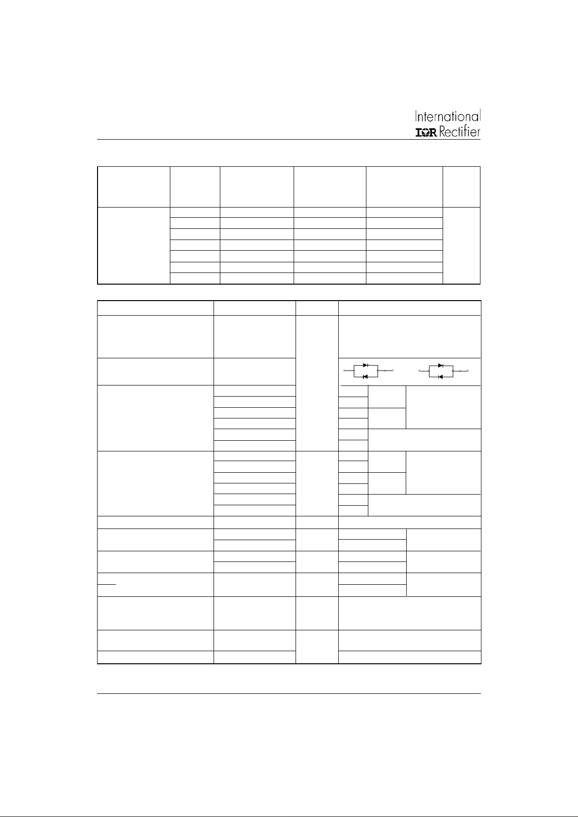
Voltage Ratings
V
, maximum V
RRM
Type number
Voltage repetitive non-repetitive peak off-state voltage, I
Code peak reverse voltage peak reverse voltage gate open circuit 125°C
-VVVmA
04 400 500 400
06 600 700 600
08 800 900 800
IRK.26 10 1000 1100 1000 15
12 1200 1300 1200
14 1400 1500 1400
16 1600 1700 1600
On-state Conduction
Parameters IRK.26 Units Conditions
I
Max. average on-state
T(AV)
current (Thyristors) 27 180
I
Max. average forward 27 T
F(AV)
current (Diodes)
I
Max. continuous RMS
O(RMS
)
on-state current.
As AC switch
I
Max. peak, one cycle 400 t=10ms No voltage
TSM
or non-repetitive on-state 420 t=8.3ms reapplied
I
or forward current 335 t=10ms 100% V
FSM
2
I
t Max. I2t for fusing 800 t=10ms No voltage
2
I
√t Max. I2√t for fusing (1) 8000 A2√s t= 0.1 to 10ms, no voltage reappl. TJ =TJ max
Max. value of threshold 0.92 Low level (3)
V
T(TO)
voltage (2) 0.95 High level (4)
r
Max. value of on-state 12.11 Low level (3)
t
slope resistance (2) 11.82 High level (4)
V
Max. peak on-state or I
TM
forward voltage I
V
FM
di/dt Max. non-repetitive rate TJ = 25oC, from 0.67 V
of rise of turned on 150 A/µs I
current t
I
Max. holding current 200 TJ = 25oC, anode supply = 6V,
H
Max. latching current 400 TJ = 25oC, anode supply = 6V, resistive load
I
L
(1) I2t for time t
(4) I > π x I
AV
= I2√t
x √tx(2) Average power = V
x
60
350 t=8.3ms reapplied
470 t=10ms T
490 t=8.3ms no voltage reapplied
730 t=8.3ms reapplied
560 t=10ms 100% V
510 t=8.3ms reapplied
1100 t=10ms T
1000 t=8.3ms no voltage reapplied
1.95 V
x I
T(TO)
T(AV)
2
, maximum V
RSM
A
A2s
V
mΩ
mA
+ r
x (I
t
T(RMS)
, max. repetitive I
DRM
o
conduction, half sine wave,
= 85oC
C
or
I
(RMS)
RRM
Initial T
= 25oC,
J
Initial TJ = TJ max.
RRM
= 25oC,
J
TJ = TJ max
= TJ max
T
J
= π x I
TM
T(AV)
= π x I
FM
F(AV)
=π x I
TM
< 0.5 µs, tp > 6 µs
r
T(AV)
, I
= 500mA,
g
TJ = 25oC
,
DRM
resistive load, gate open circuit
2
)
(3) 16.7% x π x I
< I < π x I
AV
Sinusoidal
half wave,
www.irf.com
= TJ max.
J
AV
RRM
DRM
I
(RMS)
Page 3
Bulletin I27130 rev. G 10/02
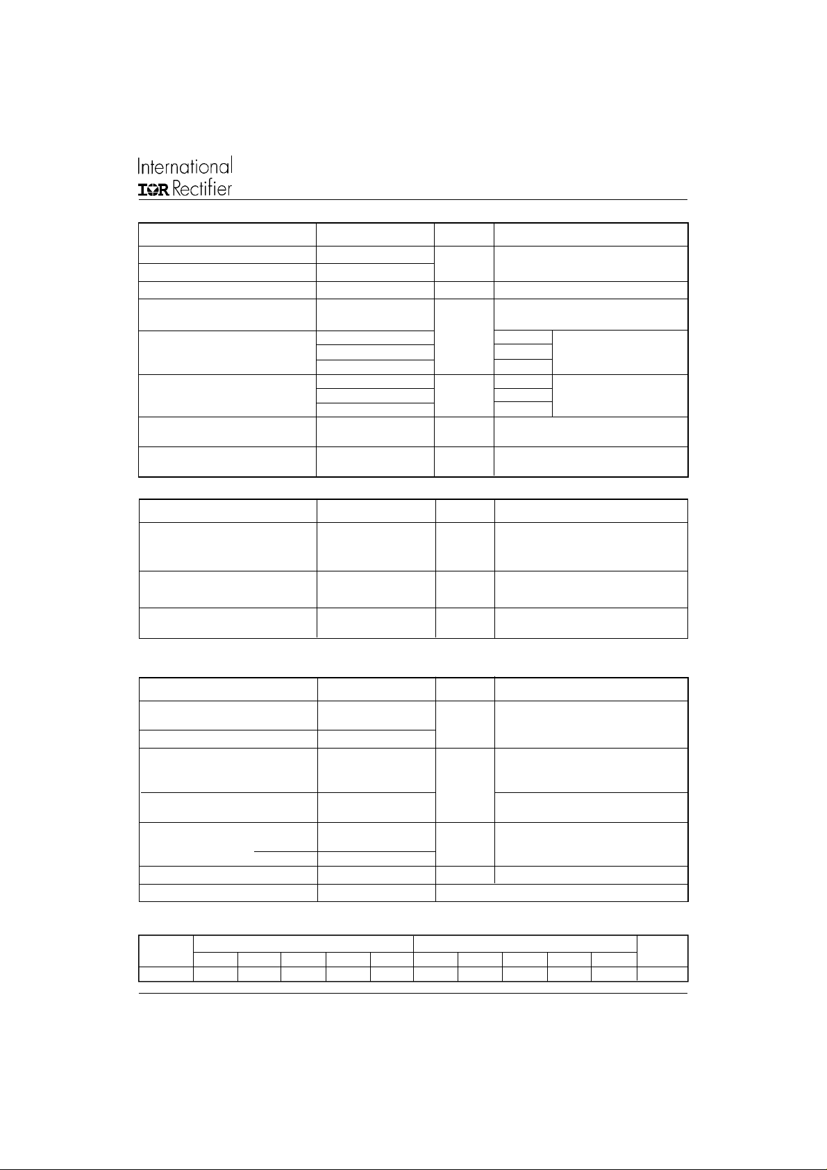
Triggering
Parameters IRK. 26 Units Conditions
PGMMax. peak gate power 10
Max. average gate power 2.5
P
G(AV)
I
Max. peak gate current 2.5 A
GM
-V
Max. peak negative
GM
gate voltage
Max. gate voltage
V
GT
required to trigger
Max. gate current
I
GT
required to trigger
Max. gate voltage
V
GD
that will not trigger
I
Max. gate current
GD
that will not trigger
10
4.0 T
2.5 T
1.7 T
270 T
150 mA TJ = 25°C
80 T
0.25 V
6mA
W
= - 40°C
V
J
= 25°C
J
= 125°C
J
= - 40°C
J
= 125°C
J
T
= 125oC,
J
rated V
= 125oC,
T
J
rated V
DRM
DRM
applied
applied
Blocking
Parameters IRK. 26 Units Conditions
Max. peak reverse and
I
RRM
I
off-state leakage current 15 mA T
DRM
at V
, V
RRM
DRM
V
RMS isolation voltage 2500 (1 min) V 50 Hz, circuit to base, all terminals
INS
3500 (1 sec) shorted
dv/dt Max. critical rate of rise 500 V/µsT
= 125oC, gate open circuit
J
= 125oC, linear to 0.67 V
J
IRK.26 Series
Anode supply = 6V
resistive load
Anode supply = 6V
resistive load
,
DRM
(5) Available with dv/dt = 1000V/µs, to complete code add S90 i.e. IRKT26/16AS90.
Thermal and Mechanical Specifications
Parameters IRK.26 Units Conditions
TJJunction operating
temperature range
T
Storage temp. range - 40 to 125
stg
Max. internal thermal
R
thJC
resistance, junction 0.31 Per module, DC operation
to case
Typical thermal resistance
R
thCS
case to heatsink
T Mounting torque ± 10%
to heatsink
busbar 3
wt Approximate weight 110 (4) gr (oz)
Case style TO-240AA JEDEC
∆R Conduction (per Junction)
(The following table shows the increment of thermal resistance R
Devices Units
180
Sine half wave conduction Rect. wave conduction
o
120
o
o
90
IRK.26 0.23 0.27 0.34 0.48 0.73 0.17 0.28 0.36 0.49 0.73 °C/W
- 40 to 125
o
60
°C
K/W
0.1
5
Nm
when devices operate at different conduction angles than DC)
thJC
o
30
180o120
Mounting surface flat, smooth and greased
A mounting compound is recommended
and the torque should be rechecked after
a period of 3 hours to allow for the
spread of the compound
o
o
90
60
o
o
30
www.irf.com
3
Page 4
IRK.26 Series
Bulletin I27130 rev. G 10/02
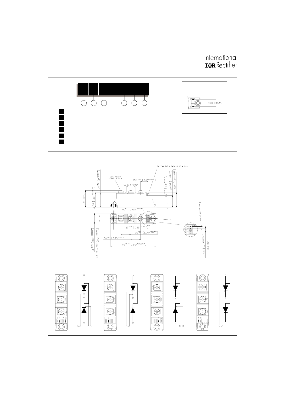
Ordering Information Table
Device Code
IRK T 26 / 16 A S90
1
2 3
1 - Module type
2 - Circuit configuration (See Circuit Configuration table below)
3 - Current code * *
4 - Voltage code (See Voltage Ratings table)
5 - A : Gen V
6 - dv/dt code: S90 = dv/dt 1000 V/µs
No letter = dv/dt 500 Vµs
5
4
Outline Table
IRK.27 types
With no auxiliary cathode
6
* * Available with no auxiliary cathode.
To specify change: 26 to 27
e.g. : IRKT27/16A etc.
Dimensions are in millimeters and [inches]
IRKT IRKH IRKL
(4) (5)
(1)
~
+
(2)
-
(3)
K1G1
K2 G2
(7)
(6)
G1
(4) (5)
(1)
~
+
(2)
-
(3)
K1
NOTE: To order the Optional Hardware see Bulletin I27900
4
(1)
~
+
(2)
-
(3)
K2
(7)G2(6)
IRKN
G1
(4) (5)
(1)
-
+
(2)
+
(3)
K1
www.irf.com
Page 5
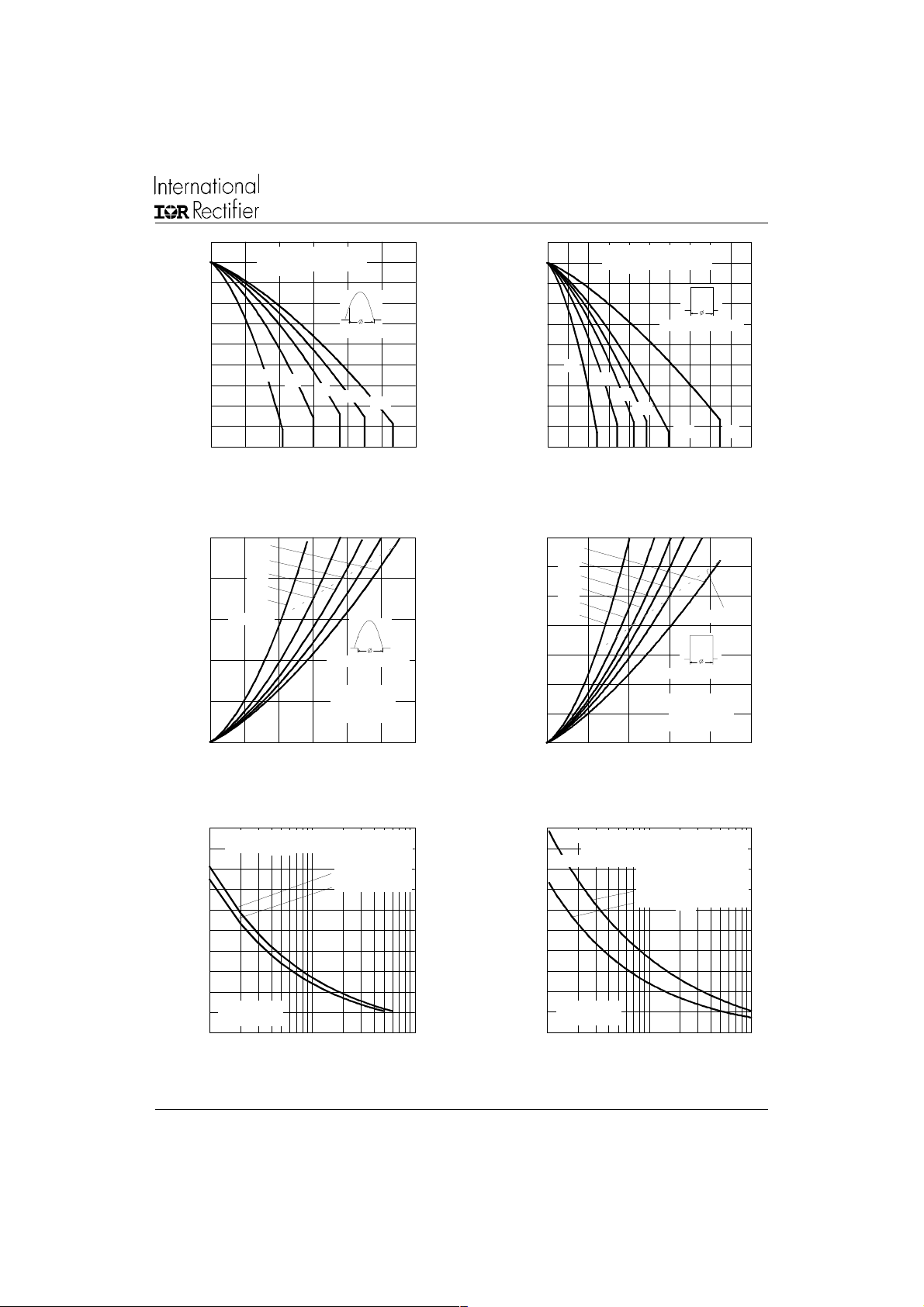
IRK.26 Series
Bulletin I27130 rev. G 10/02
130
IRK.26.. Series
R (DC) = 0.62 K/W
thJC
120
110
100
30°
90
80
Maxi mum Allowable Case Temperatur e (°C)
0 5 10 15 20 25 30
Conduction A ng le
60°
90°
120°
Average On-state Current (A)
180°
130
120
110
100
90
80
Maximum Allowable Case Temperature (°C)
0 1020304050
IRK.26.. Series
R (DC) = 0.62 K/W
thJC
Conduct ion Pe ri od
30°
60°
90°
120°
Average On-s tate C urrent (A)
Fig. 1 - Current Ratings Characteristics Fig. 2 - Current Ratings Characteristics
50
180°
120°
40
30
20
10
0
Maximum Average On-state Power Loss (W)
90°
60°
30°
RMS Limit
Conducti on A ngle
IRK.26.. Series
Per Junction
T = 125°C
J
0 5 10 15 20 25 30
Aver age On-sta te Current (A)
70
DC
180°
60
120°
90°
50
60°
30°
40
30
20
Conduction Period
10
0
Maximum Average On-state Power Loss (W)
01020304050
Average On-s tate Curre nt (A)
Fig. 3 - On-state Power Loss Characteristics Fig. 4 - On-state Power Loss Characteristics
180°
RMS Limit
IRK.26.. Series
Per Junction
T = 125°C
J
DC
400
At Any Rated Load Condition And With
Rated V Applied Following Surge.
RRM
350
Initial T = 125°C
J
@ 60 Hz 0.0083 s
@ 50 Hz 0.0100 s
300
250
200
IRK.26.. Series
Peak Half Si ne Wave On-state Current (A)
Per Junction
150
1 10 100
Number Of Equal Amplitude Half Cycle Current Pulses (N)
400
Maximum Non Repetitive Surge Current
Versus Pulse Train Duration. Control
Of Conduction May Not Be Maintained.
350
No Voltage Reapplied
300
250
200
IRK.26.. Series
Peak Half Sine Wave On-state Current (A)
Per Junctio n
150
0.01 0.1 1
Pulse Train Duration (s)
Rated V Reapplied
Fig. 5 - Maximum Non-Repetitive Surge Current Fig. 6 - Maximum Non-Repetitive Surge Current
www.irf.com
Initial T = 125°C
J
RRM
5
Page 6
IRK.26 Series
Bulletin I27130 rev. G 10/02
100
90
80
70
180°
120°
90°
60°
30°
60
50
40
Conduction Angle
30
20
10
Maximum Total On-state Power Loss (W)
0
0
10 20 30 40 50 60
IRK.26.. Series
Per Module
T = 125°C
J
Total RMS Output Current (A)
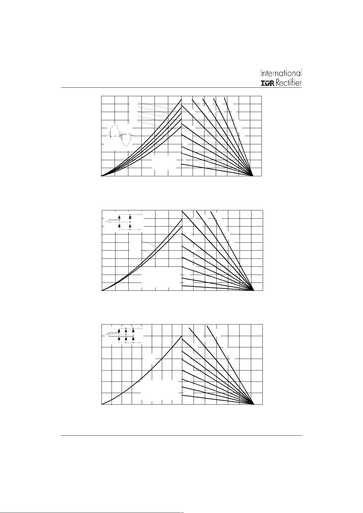
Fig. 7 - On-state Power Loss Characteristics
250
200
150
100
50
Maximum Total Power Loss (W)
0
0 102030405060
180°
(Sine)
180°
(Rect)
2 x IRK.26.. Series
Single Phase Bridge
Connected
T = 125°C
J
Total Output C urrent (A )
Fig. 8 - On-state Power Loss Characteristics
R
0
0
.
0
5
.
7
K
1
/
W
K
/
W
1
.
5
K
/
W
2
K
/
W
3
K
/
W
4
K
/
W
8
K/
W
t
.
h
3
S
K
A
K
/
W
/
W
=
0
.
1
K
/
W
D
e
l
t
a
R
0 20 40 60 80 100 120 140
Maximum Allowab l e Ambient Temperat ure (°C)
R
t
0
h
.
S
2
0
.
3
K
/
W
0
.
5
K
/
W
0
.
7
K
/
W
1
K
/
W
1
.
5
K
/
W
3
K/
W
8
K
/
W
A
K
/
=
W
0
.
1
K
/
W
-
D
e
l
t
a
R
0 20 40 60 80 100 120 140
Maximum Allowabl e Ambient Temperature (°C)
350
300
250
200
120°
(Rect)
150
100
3 x IRK.26.. Series
Three Phase Bridge
Maximum Total Power Loss (W)
50
0
0 1020304050607080
Connected
T = 125°C
J
Total Output Current (A)
0
.
3
K
/
W
0
.
4
K
/
W
0.
5
K
/
W
0
.
7
K
/
W
1
K
/
W
1
.
5
K
/
W
3
K
/
W
0 20406080100120140
Maximum Allowable Ambient Temperatur e (°C)
R
t
h
0
S
.
A
2
K
=
/
W
0
.
1
K
/
W
D
e
l
t
a
R
Fig. 9 - On-state Power Loss Characteristics
6
www.irf.com
Page 7
1
thJC
0.1
1000
100
10
Instantaneous On-state Current (A)
1
01234567
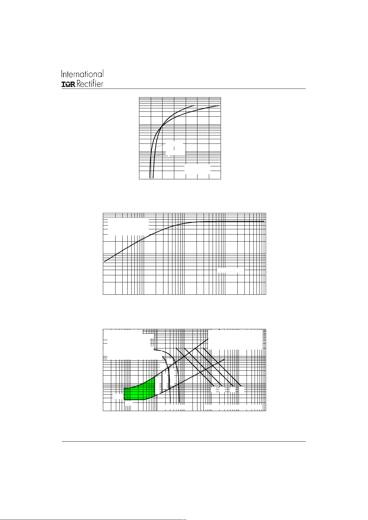
Fig. 10 - On-state Voltage Drop Characteristics
Steady State Value:
R = 0.62 K/W
thJC
(DC Operation)
T = 25°C
J
T = 125°C
J
IRK.26.. Series
Per Junction
Insta ntaneous O n -state Voltage (V)
IRK.26 Series
Bulletin I27130 rev. G 10/02
www.irf.com
IRK.26.. Series
Transient Thermal Impeda nce Z (K/W)
0.01
0.001 0.01 0.1 1 10
Square Wave Pulse Duration (s)
Characteristics
thJC
(1) PGM = 100 W, tp = 500 µs
(2) PGM = 50 W, tp = 1 ms
(3) PGM = 20 W, tp = 25 ms
(4) PGM = 10 W, tp = 5 ms
100
Rectangular gate pulse
a)Recommended load line for
rated di/dt: 20 V, 30 ohms
tr = 0.5 µs, tp >= 6 µs
b)Recommended load line for
<= 30% rated di/dt: 20 V, 65 ohms
10
tr = 1 µs, tp >= 6 µs
Fig. 11 - Thermal Impedance Z
(a)
(b)
TJ = -40 °C
TJ = 25 °C
TJ = 125 °C
1
(3) (2) (1)
(4)
Instantaneous Gate Voltage (V)
VGD
IGD
0.1
0.001 0.01 0.1 1 10 100 1000
IRK.26.. Series
Frequency Li m ited by PG(AV)
Instantaneous Gate Current (A)
Fig. 12- Gate Characteristics
7
Page 8

IRK.26 Series
Bulletin I27130 rev. G 10/02
This product has been designed and qualified for Industrial Level.
IR WORLD HEADQUARTERS: 233 Kansas St., El Segundo, California 90245, USA Tel: (310) 252-7105
8
Data and specifications subject to change without notice.
Qualification Standards can be found on IR's Web site.
TAC Fax: (310) 252-7309
Visit us at www.irf.com for sales contact information. 10/02
www.irf.com
 Loading...