

Page 1
查询IRHE9130供应商
RADIATION HARDENED
POWER MOSFET
SURFACE MOUNT (LCC-18)
Product Summary
Part Number Radiation Level RDS(on) ID QPL Part Number
IRHE9130 100K Rads (Si) 0.30Ω -6.5A JANSR2N7389U
IRHE93130 300K Rads (Si) 0.30Ω -6.5A JANSF2N7389U
PD - 90881C
IRHE9130
100V, P-CHANNEL
REF: MIL-PRF-19500/630
RAD-Hard
MOSFET TECHNOLOGY
™
HEXFET
®
International Rectifier’s RAD-HardTM HEXFET
technology provides high performance power MOSFETs
®
MOSFET
for space applications. This technology has over a decade of proven performance and reliability in satellite
applications. These devices have been characterized
for both Total Dose and Single Event Effects (SEE). The
combination of low Rdson and low gate charge reduces
the power losses in switching applications such as DC to
DC converters and motor control. These devices retain
all of the well established advantages of MOSFETs such
as voltage control, fast switching, ease of paralleling and
temperature stability of electrical parameters.
Absolute Maximum Ratings
Features:
n Single Event Effect (SEE) Hardened
n Low RDS(on)
n Low Total Gate Charge
n Proton Tolerant
n Simple Drive Requirements
n Ease of Paralleling
n Hermetically Sealed
n Ceramic Package
n Surface Mount
n Light Weight
LCC - 18
Pre-Irradiation
Parameter Units
ID @ VGS = 12V, TC = 25°C Continuous Drain Current -6.5
ID @ VGS = 12V, TC = 100°C Continuous Drain Current -4.1
I
DM
PD @ TC = 25°C Max. Power Dissipation 25 W
V
GS
E
AS
I
AR
E
AR
dv/dt Peak Diode Recovery dv/dt ➂ -22
T
J
T
STG
Pulsed Drain Current ➀ -26
Linear Derating Factor 0.2 W/°C
Gate-to-Source Voltage ±20 V
Single Pulse Avalanche Energy ➁ 165 mJ
Avalanche Current ➀ -6.5 A
Repetitive Avalanche Energy ➀ 2.5 mJ
Operating Junction -55 to 150
Storage Temperature Range
Pckg. Mounting Surface Temp. 300 ( for 5s)
Weight 0.42 (Typical) g
A
V/ns
o
C
For footnotes refer to the last page
www.irf.com 1
2/20/03
Page 2
IRHE9130 Pre-Irradiation
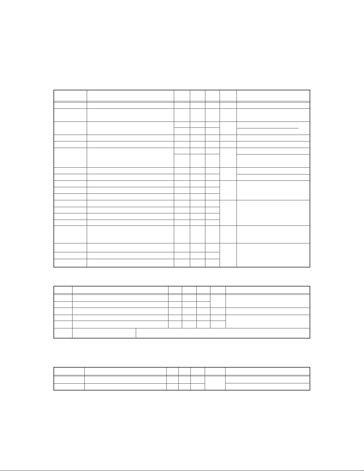
Electrical Characteristics @ Tj = 25°C (Unless Otherwise Specified)
Parameter Min Typ Max Units Test Conditions
BV
DSS
∆BV
R
DS(on)
V
GS(th)
g
fs
I
DSS
I
GSS
I
GSS
Q
g
Q
gs
Q
gd
t
d(on)
t
r
t
d(off)
t
f
L
S + LD
DSS
Drain-to-Source Breakdown Voltage -100 — — V VGS =0 V, ID = -1.0mA
/∆TJTemperature Coefficient of Breakdown — -0.112 — V/°C Reference to 25°C, ID = -1.0mA
Voltage
Static Drain-to-Source — — 0.30 VGS = -12V, ID = -4.1A
On-State Resistance — — 0.35
Gate Threshold Voltage -2.0 — -4.0 V VDS = VGS, ID = -1.0mA
Forward Transconductance 2.5 — — S ( )VDS > -15V, IDS = -4.1A
Zero Gate Voltage Drain Current — — - 25 VDS= -80V,VGS=0V
— — -250 VDS = -80V
Gate-to-Source Leakage Forward — — -100 VGS = -20V
Gate-to-Source Leakage Reverse — — 100 VGS = 20V
Total Gate Charge — — 45 VGS = -12V, ID = -6.5A
Gate-to-Source Charge — — 10 nC VDS = -50V
Gate-to-Drain (‘Miller’) Charge — — 25
Turn-On Delay Time — — 30 VDD = -50V, ID = -6.5A,
Rise Time — — 50 VGS = -12V, RG = 7.5Ω
Turn-Off Delay Time — — 70
Fall Time — — 70
Total Inductance — 6.1 —
Ω
µA
nA
ns
nH
VGS = -12V, ID = -6.5A
Ω
VGS = 0V, TJ = 125°C
Measured from the center of
drain pad to center of source pad
C
iss
C
oss
C
rss
Input Capacitance — 1200 — VGS = 0V, VDS = -25V
Output Capacitance — 290 — pF f = 1.0MHz
Reverse Transfer Capacitance — 76 —
Source-Drain Diode Ratings and Characteristics
Parameter Min Typ Max Units Test Conditions
I
Continuous Source Current (Body Diode) — — -6.5
S
I
Pulse Source Current (Body Diode) ➀ — — -26
SM
V
Diode Forward Voltage — — -3.0 V Tj = 25°C, IS = -6.5A, VGS = 0V ➃
SD
t
Reverse Recover y Time — — 250 nS Tj = 25°C, IF = -6.5A, di/dt ≤ -100A/µs
rr
Q
Reverse Recovery Charge — — 0.74 µC VDD ≤ -25V ➃
RR
t
Forward Turn-On Time Intrinsic turn-on time is negligible. Turn-on speed is substantially controlled by L
on
A
S
Thermal Resistance
Parameter Min Typ Max Units Test Conditions
R
thJC
R
thJPCB
Note: Corresponding Spice and Saber models are available on the G&S Website.
For footnotes refer to the last page
2 www.irf.com
Junction-to-Case — — 5.0
Junction-to-PC Board — 19 — Solder to a copper clad PC Board
°C/W
+ LD.
Page 3
Radiation Characteristics
Pre-Irradiation IRHE9130
International Rectifier Radiation Hardened MOSFETs are tested to verify their radiation hardness capability .
The hardness assurance program at International Rectifier is comprised of two radiation environments.
Every manufacturing lot is tested for total ionizing dose (per notes 5 and 6) using the TO-3 package. Both
pre- and post-irradiation performance are tested and specified using the same drive circuitry and test
conditions in order to provide a direct comparison.
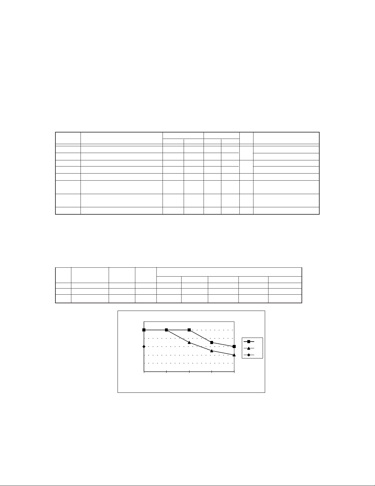
T able 1. Electrical Characteristics @ Tj = 25°C, P ost Total Dose Irradiation ➄➅
Parameter 100K Rads(Si)
BV
Drain-to-Source Breakdown Voltage -100 — -100
DSS
V
GS(th)
I
GSS
I
GSS
I
DSS
R
DS(on)
Gate Threshold Voltage - 2.0 - 4.0 -2.0 -5.0 VGS = VDS, ID = -1.0mA
Gate-to-Source Leakage Forward — -100 — -100
Gate-to-Source Leakage Reverse — 100 — 100 VGS = 20 V
Zero Gate Voltage Drain Current — -25 — -25 µA VDS=-80V, V
Static Drain-to-Source ➃ — 0.259 — 0.259 Ω VGS = -12V, ID =-4.1A
Min Max Min Max
1
300K Rads (Si)
On-State Resistance (TO-3)
R
DS(on)
Static Drain-to-Source ➃ — 0.30 — 0.30 Ω VGS = -12V, ID =-4.1A
On-State Resistance (LCC-18)
V
SD
1. Part number IRHE9130 (JANSR2N7389U)
2. Part number IRHE93130 (JANSF2N7389U)
Diode Forward Voltage ➃ — -3.0 — -3.0 V VGS = 0V, IS = -6.5A
International Rectifier radiation hardened MOSFETs have been characterized in heavy ion environment for
Single Event Effects (SEE). Single Event Effects characterization is illustrated in Fig. a and Table 2.
2
Units
— V
nA
Test Conditions
VGS = 0V, ID = -1.0mA
VGS = -20V
=0V
GS
T able 2. Single Event Effect Safe Operating Area
Io n LET Energy Range VDS(V)
MeV/(mg/cm2)) (MeV) (µm) @VGS=0V @VGS=5V @VGS=10V @VGS=15V @VGS=20V
Cu 28 285 43 -100 -100 -100 -70 -60
Br 36.8 305 39 -100 -100 -70 -50 -40
I 59.8 343 32.6 -60 — — — —
-120
-100
-80
-60
VDS
-40
-20
0
0 5 10 15 20
VGS
Cu
Br
I
Fig a. Single Event Effect, Safe Operating Area
For footnotes refer to the last page
www.irf.com 3
Page 4
IRHE9130 Pre-Irradiation
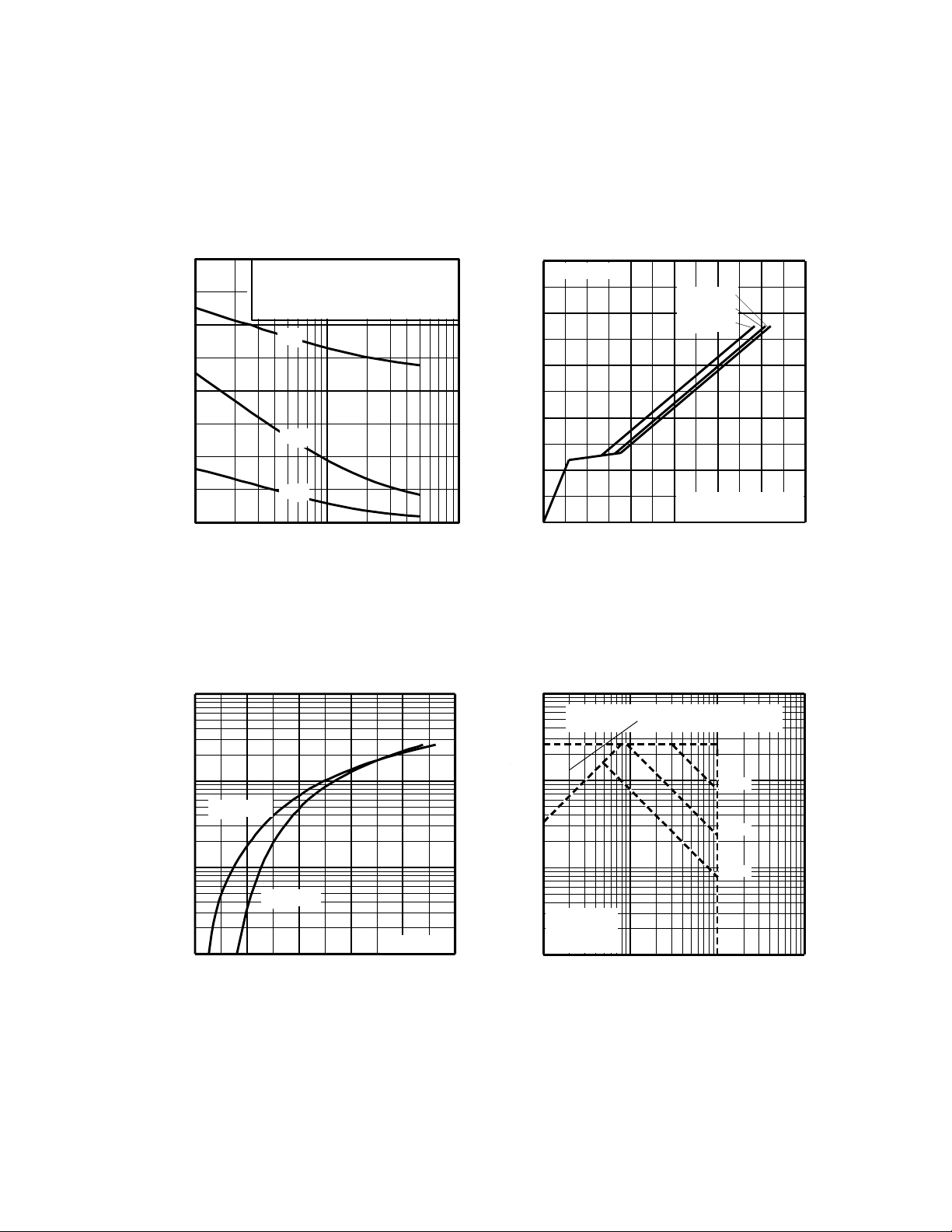
100
10
D
-I , Drain-to-Source Current (A)
1
100
VGS
TOP
-15V
-12V
-10V
-9.0V
-8.0V
-7.0V
-6.0V
BOTTOM
-5.0V
-5.0V
20µs PULSE WIDTH
1 10 100
-V , Drain-to-Source Voltage (V)
DS
°
T = 25 C
J
100
10
D
-I , Drain-to-Source Current (A)
1
VGS
TOP
-15V
-12V
-10V
-9.0V
-8.0V
-7.0V
-6.0V
BOTTOM
-5.0V
-5.0V
20µs PULSE WIDTH
T = 150 C
1 10 100
-V , Drain-to-Source Voltage (V)
DS
°
J
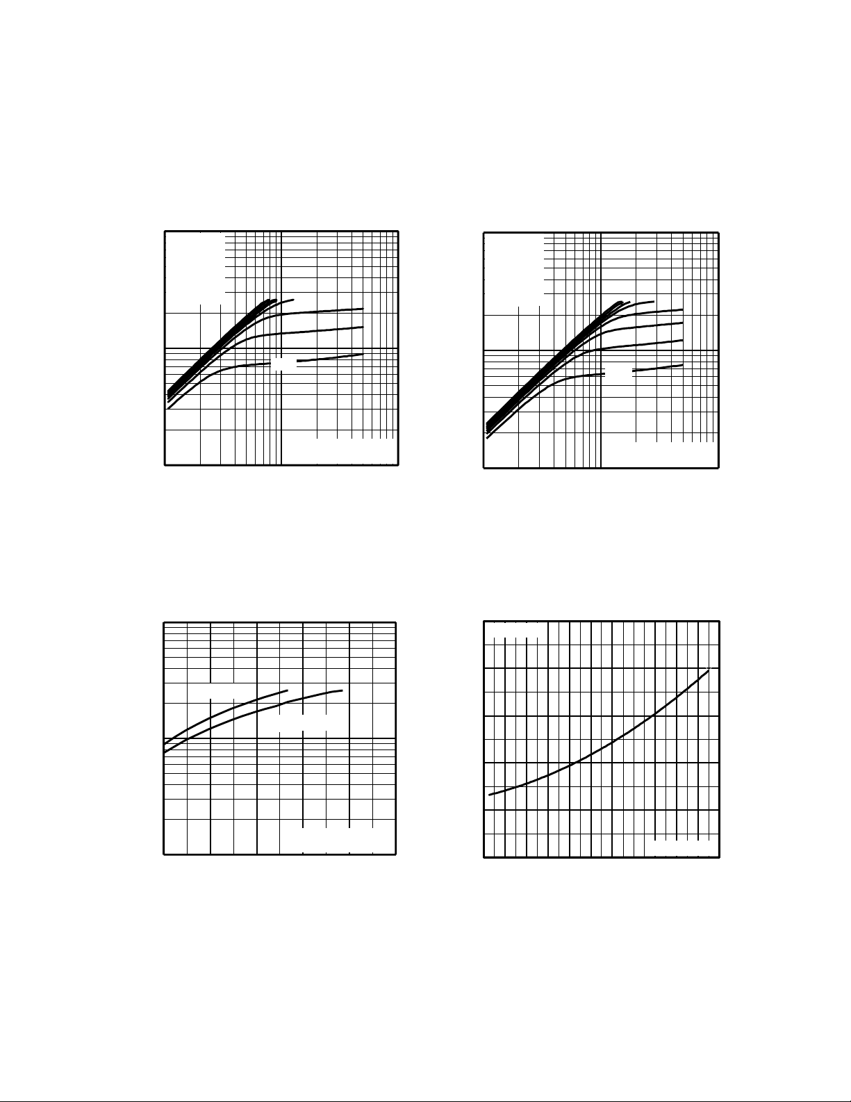
Fig 2. Typical Output CharacteristicsFig 1. Typical Output Characteristics
2.5
-6.5A
I =
D
2.0
°
T = 25 C
J
°
T = 150 C
10
D
-I , Drain-to-Source Current (A)
1
5 6 7 8 9 10
-V , Gate-to-Source Voltage (V)
GS
J
V = -50V
DS
20µs PULSE WIDTH
Fig 3. Typical Transfer Characteristics
1.5
1.0
(Normalized)
0.5
DS(on)
R , Drain-to-Source On Resistance
0.0
-60 -40 -20 0 20 40 60 80 100 120 140 160
T , Junction Temperature ( C)
J
Fig 4. Normalized On-Resistance
V =
-12V
GS
°
Vs. Temperature
4 www.irf.com
Page 5
Pre-Irradiation IRHE9130
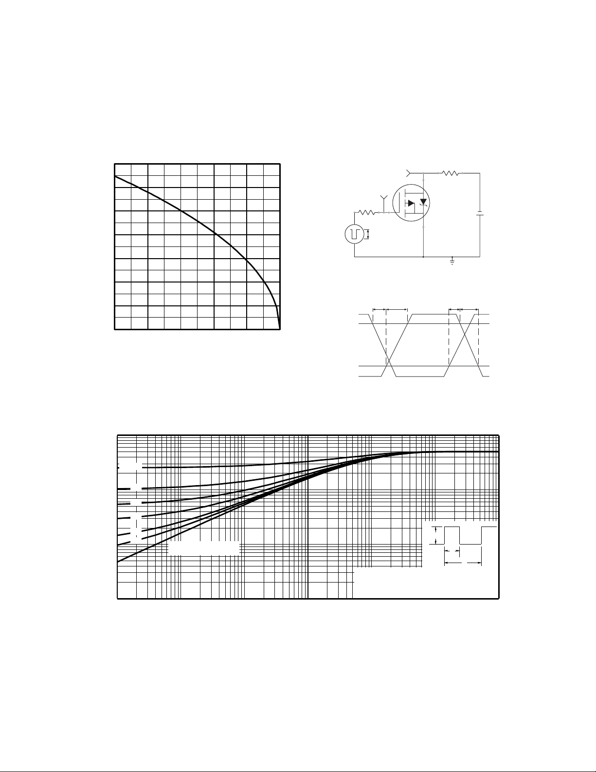
)
2000
1500
1000
C, Capacitance (pF)
500
0
1 10 100
V
=
0V,
GS
C
=
issgsgd , ds
C
=
rssgd
C
=
oss dsgd
C
iss
C
oss
C
rss
-V , Drain-to-Source Voltage (V)
DS
f = 1MHz
C
+ C
C
C
C SHORTED
+ C
Fig 5. Typical Capacitance Vs.
Drain-to-Source Voltage
100
20
I =
-6.5
D
V =-80V
DS
V =-50V
16
12
8
4
GS
-V , Gate-to-Source Voltage (V)
0
0 10 20 30 40 50 60
Q , Total Gate Charge (nC)
G
DS
V =-20V
DS
FOR TEST CIRCUIT
SEE FIGURE
Fig 6. Typical Gate Charge Vs.
Gate-to-Source Voltage
100
OPERATION IN THIS AREA LIMITED
BY R
DS(on
13
10
°
T = 150 C
J
1
°
T = 25 C
SD
-I , Reverse Drain Current (A)
0.1
0.2 1.0 1.8 2.6 3.4 4.2
J
V = 0 V
GS
-V ,Source-to-Drain Voltage (V)
SD
Fig 7. Typical Source-Drain Diode
10
1
D
-I , Drain Current (A)I , Drain Current (A)
°
= 25 C
C
T T= 150 C
Single Pulse
0.1
1 10 100 1000
°
J
-V , Drain-to-Source Voltage (V)
DS
100us
1ms
10ms
Fig 8. Maximum Safe Operating Area
Forward Voltage
www.irf.com 5
Page 6
IRHE9130 Pre-Irradiation
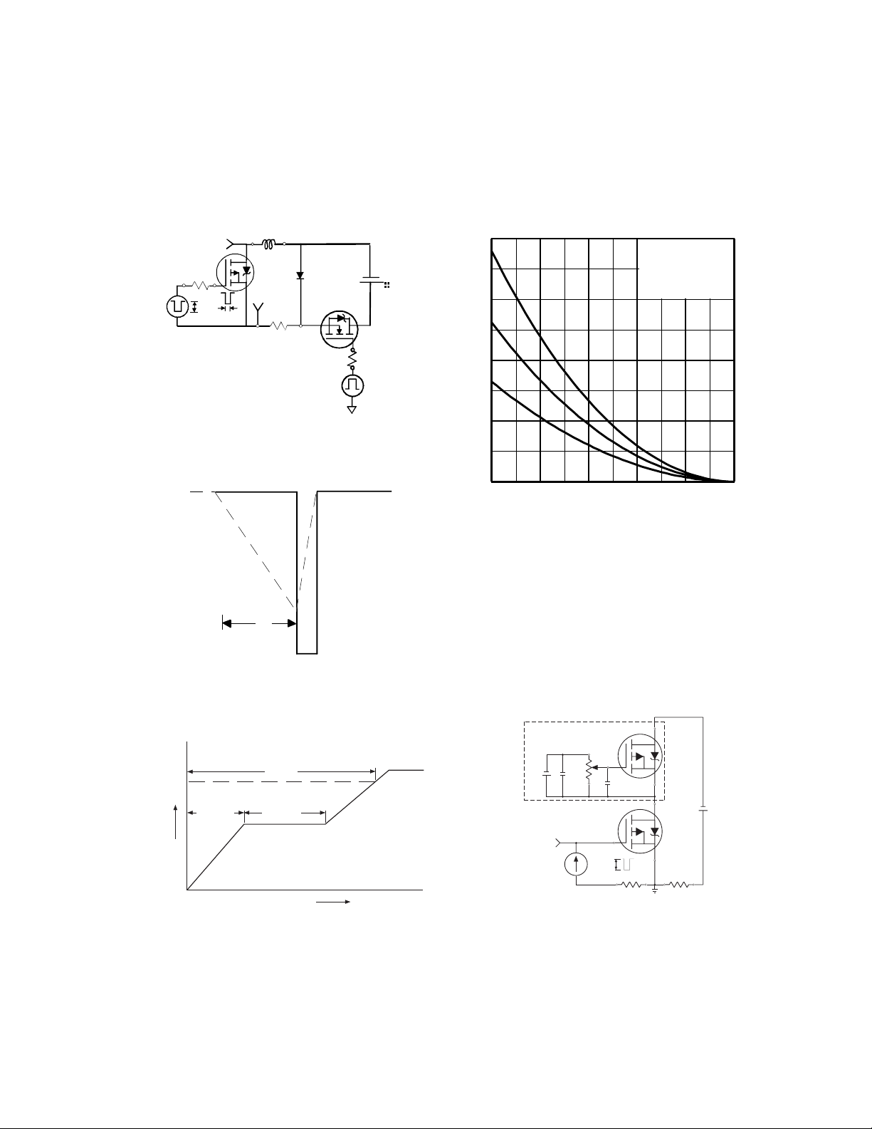
R
D.U.T.
D
-
+
V
DD
7.0
6.0
5.0
V
DS
V
GS
R
G
4.0
3.0
D
2.0
-I , Drain Current (A)
1.0
0.0
25 50 75 100 125 150
T , Case Temperature ( C)
C
°
Fig 9. Maximum Drain Current Vs.
Fig 10a. Switching Time Test Circuit
V
10%
90%
V
V
Pulse Width ≤ 1 µs
Duty Factor ≤ 0.1 %
t
d(on)tr
GS
DS
GS
t
d(off)tf
Case Temperature
Fig 10b. Switching Time Waveforms
10
D = 0.50
thJC
Thermal Response (Z )
0.20
1
0.10
0.05
0.02
0.01
0.1
0.01
0.00001 0.0001 0.001 0.01 0.1 1 10
SINGLE PULSE
(THERMAL RESPONSE)
Notes:
1. Duty factor D = t / t
2. Peak T =P x Z + T
t , Rectangular Pulse Duration (sec)
1
J DM thJC C
P
DM
t
1 2
1
t
2
Fig 11. Maximum Effective Transient Thermal Impedance, Junction-to-Case
6 www.irf.com
Page 7
Pre-Irradiation IRHE9130
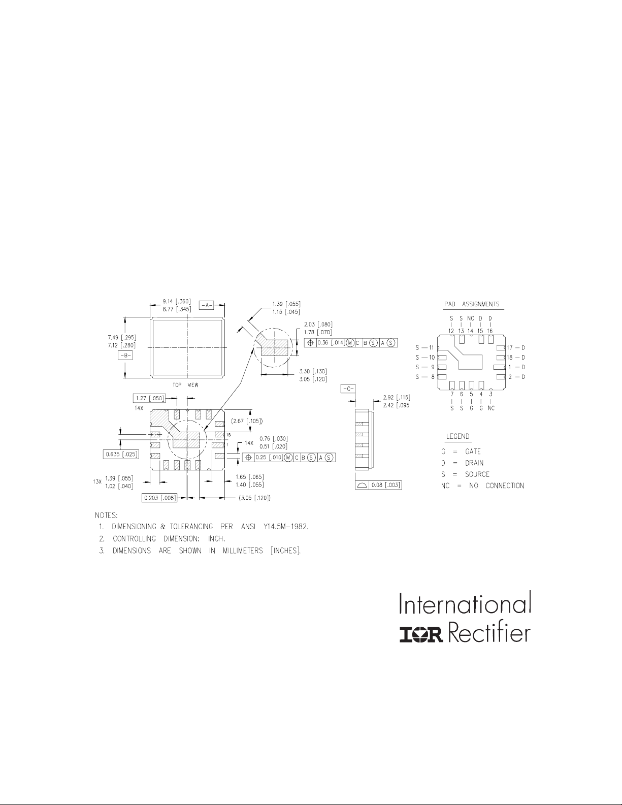
(BR)
L
D.U.T
I
AS
0.01
t
p
DRIVER
Ω
15V
V
DD
R
-20V
V
DS
G
V
GS
Fig 12a. Unclamped Inductive Test Circuit
I
AS
t
p
V
DSS
400
TOP
A
300
200
100
AS
E , Single Pulse Avalanche Energy (mJ)
0
25 50 75 100 125 150
Starting T , Junction Temperature ( C)
J
BOTTOM
I
D
-2.9A
-4.1A
-6.5A
°
Fig 12c. Maximum Avalanche Energy
Vs. Drain Current
Fig 12b. Unclamped Inductive Waveforms
Current Regulator
Same Type as D.U.T.
Q
G
-12V
Q
GS
V
G
Q
GD
Charge
Fig 13a. Basic Gate Charge Waveform
-12V
12V
V
GS
Fig 13b. Gate Charge Test Circuit
50KΩ
.2µF
.3µF
-3mA
Current Sampling Resistors
V
DS
+
D.U.T.
I
G
I
D
www.irf.com 7
Page 8
IRHE9130 Pre-Irradiation
Footnotes:
➀ Repetitive Rating; Pulse width limited by
maximum junction temperature.
➁ V
= -25V, starting TJ = 25°C, L= 7.8mH
DD
Peak IL = -6.5A, VGS = -12V
➂ I
≤ -6.5A, di/dt ≤ -430A/ µs,
SD
VDD ≤ -100V, TJ ≤ 150°C
➃ Pulse width ≤ 300 µs; Duty Cycle ≤ 2%
➄ Total Dose Irradiation with V
-12 volt VGS applied and VDS = 0 during
irradiation per MIL-STD-750, method 1019, condition A.
➅ Total Dose Irradiation with V
-80 volt VDS applied and VGS = 0 during
irradiation per MlL-STD-750, method 1019, condition A.
GS
DS
Bias.
Bias.
Case Outline and Dimensions — LCC-18
IR WORLD HEADQUARTERS: 233 Kansas St., El Segundo, California 90245, USA Tel: (310) 252-7105
TAC Fax: (310) 252-7903
Visit us at www.irf.com for sales contact information.
Data and specifications subject to change without notice. 02/03
8 www.irf.com
 Loading...