

Page 1
PD - 9.1112
Next Data SheetIndex
Previous Datasheet
To Order
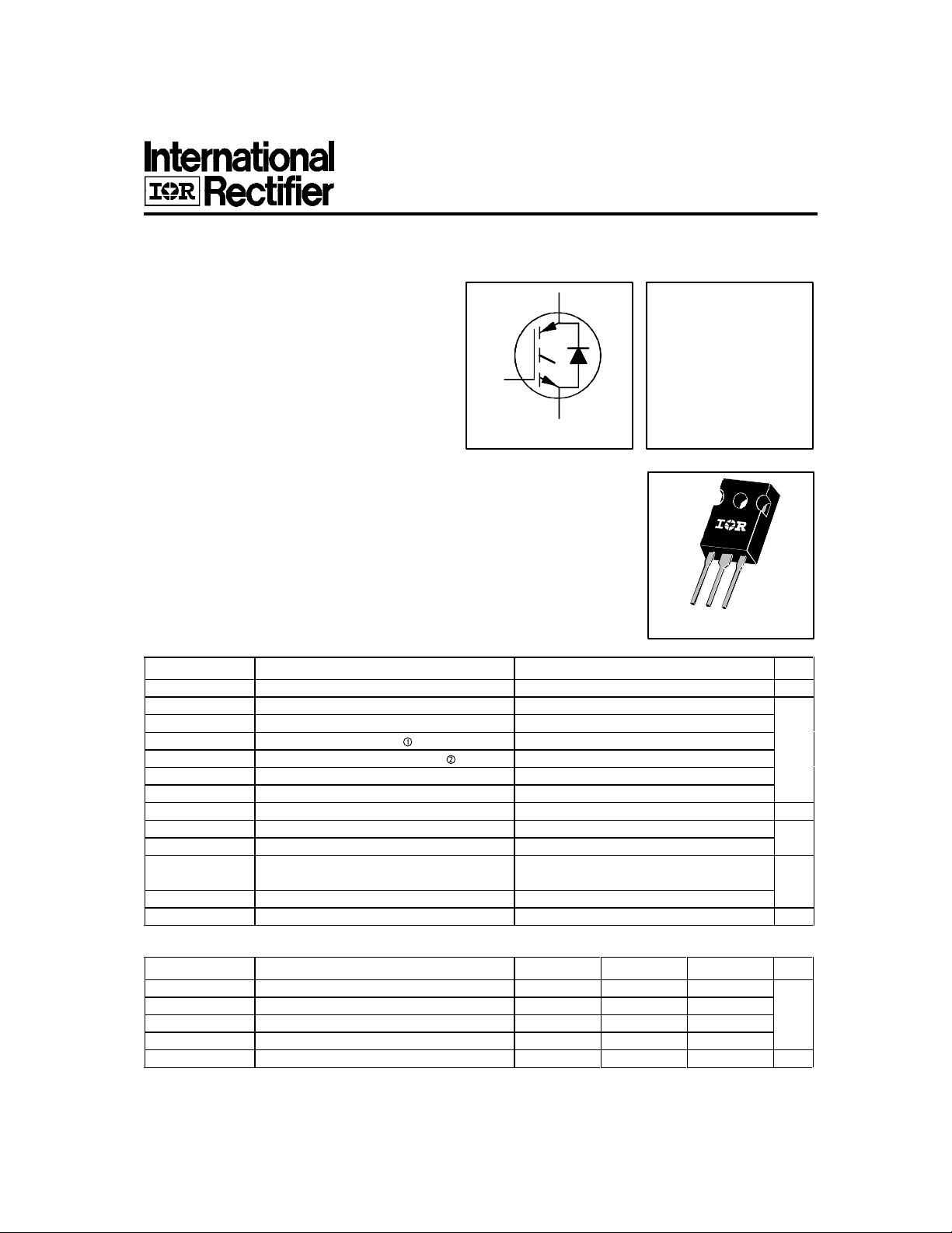
IRGPC30UD2
INSULATED GATE BIPOLAR TRANSISTOR
UltraFast CoPack IGBT
WITH ULTRAFAST SOFT RECOVERY DIODE
Features
• Switching-loss rating includes all "tail" losses
• HEXFREDTM soft ultrafast diodes
• Optimized for high operating frequency (over 5kHz)
See Fig. 1 for Current vs. Frequency curve
G
C
V
= 600V
CES
V
CE(sat)
≤ 3.0V
@VGE = 15V, IC = 12A
E
n-channel
Description
Co-packaged IGBTs are a natural extension of International Rectifier's well
known IGBT line. They provide the convenience of an IGBT and an ultrafast
recovery diode in one package, resulting in substantial benefits to a host of
high-voltage, high-current, motor control, UPS and power supply applications.
O-247AC
T
Absolute Maximum Ratings
Parameter Max. Units
V
CES
IC @ TC = 25°C Continuous Collector Current 23
IC @ TC = 100°C Continuous Collector Current 12
I
CM
I
LM
IF @ TC = 100°C Diode Continuous Forward Current 12
I
FM
V
GE
PD @ TC = 25°C Maximum Power Dissipation 100 W
PD @ TC = 100°C Maximum Power Dissipation 42
T
J
T
STG
Collector-to-Emitter Voltage 600 V
Pulsed Collector Current 92 A
Clamped Inductive Load Current 92
Diode Maximum Forward Current 92
Gate-to-Emitter Voltage ± 20 V
Operating Junction and -55 to +150
Storage Temperature Range °C
Soldering Temperature, for 10 sec. 300 (0.063 in. (1.6mm) from case)
Mounting Torque, 6-32 or M3 Screw. 10 lbf•in (1.1 N•m)
Thermal Resistance
R
θJC
R
θJC
R
θCS
R
θJA
Wt Weight — 6 (0.21) — g (oz)
Parameter Min. Typ. Max. Units
Junction-to-Case - IGBT — — 1.2
Junction-to-Case - Diode — — 2.5 °C/W
Case-to-Sink, flat, greased surface — 0.24 —
Junction-to-Ambient, typical socket mount — — 40
Revision 1
C-709
Page 2
IRGPC30UD2
Next Data SheetIndex
Previous Datasheet
To Order
Electrical Characteristics @ TJ = 25°C (unless otherwise specified)
Parameter Min. Typ. Max. Units Conditions
V
(BR)CES
∆V
(BR)CES
V
CE(on)
V
GE(th)
∆V
GE(th)
g
fe
I
CES
V
FM
I
GES
Switching Characteristics @ TJ = 25°C (unless otherwise specified)
Parameter Min. Typ. Max. Units Conditions
Q
g
Q
ge
Q
gc
t
d(on)
t
r
t
d(off)
t
f
E
on
E
off
E
ts
t
d(on)
t
r
t
d(off)
t
f
E
ts
L
E
C
ies
C
oes
C
res
t
rr
I
rr
Q
rr
di
(rec)M
Notes:
Repetitive rating; VGE=20V, pulse width
limited by max. junction temperature.
( See fig. 20 )
Collector-to-Emitter Breakdown Voltage 600 — — V VGE = 0V, IC = 250µA
/∆T
Temp. Coeff. of Breakdown Voltage — 0.63 — V/°C VGE = 0V, IC = 1.0mA
J
Collector-to-Emitter Saturation Voltage — 2.2 3.0 IC = 12A VGE = 15V
— 2.7 — V IC = 23A See Fig. 2, 5
— 2.4 — IC = 12A, TJ = 150°C
Gate Threshold Voltage 3.0 — 5.5 VCE = VGE, IC = 250µA
/∆TJTemp. Coeff. of Threshold Voltage — -11 — mV/°C VCE = VGE, IC = 250µA
Forward Transconductance 3.1 8.6 — S VCE = 100V, IC = 12A
Zero Gate Voltage Collector Current — — 250 µA VGE = 0V, VCE = 600V
— — 2500 VGE = 0V, VCE = 600V, TJ = 150°C
Diode Forward Voltage Drop — 1.4 1.7 V IC = 12A See Fig. 13
— 1.3 1.6 IC = 12A, TJ = 150°C
Gate-to-Emitter Leakage Current — — ±100 nA VGE = ±20V
Total Gate Charge (turn-on) — 29 36 IC = 12A
Gate - Emitter Charge (turn-on) — 4.8 6.8 nC VCC = 400V
Gate - Collector Charge (turn-on) — 12 17 See Fig. 8
Turn-On Delay Time — 67 — TJ = 25°C
Rise Time — 56 — ns IC = 12A, VCC = 480V
Turn-Off Delay Time — 170 250 VGE = 15V, RG = 23Ω
Fall Time — 140 270 Energy losses include "tail" and
Turn-On Switching Loss — 0.70 — diode reverse recovery.
Turn-Off Switching Loss — 0.80 — mJ See Fig. 9, 10, 11, 18
Total Switching Loss — 1.5 2.5
Turn-On Delay Time — 61 — TJ = 150°C, See Fig. 9, 10, 11, 18
Rise Time — 51 — ns IC = 12A, VCC = 480V
Turn-Off Delay Time — 190 — VGE = 15V, RG = 23Ω
Fall Time — 190 — Energy losses include "tail" and
Total Switching Loss — 1.9 — mJ diode reverse recovery.
Internal Emitter Inductance — 13 — nH Measured 5mm from package
Input Capacitance — 680 — VGE = 0V
Output Capacitance — 110 — pF VCC = 30V See Fig. 7
Reverse Transfer Capacitance — 11 — ƒ = 1.0MHz
Diode Reverse Recovery Time — 42 60 ns TJ = 25°C See Fig.
— 80 120 TJ = 125°C 14 IF = 12A
Diode Peak Reverse Recovery Current — 3.5 6.0 A TJ = 25°C See Fig.
— 5.6 10 TJ = 125°C 15 VR = 200V
Diode Reverse Recovery Charge — 80 180 nC TJ = 25°C See Fig.
— 220 600 TJ = 125°C 16 di/dt = 200A/µs
/dt Diode Peak Rate of Fall of Recovery — 180 — A/µs TJ = 25°C See Fig.
During t
b
— 120 — TJ = 125°C 17
VCC=80%(V
), VGE=20V, L=10µH,
CES
RG= 23Ω, ( See fig. 19 )
Pulse width 5.0µs,
single shot.
Pulse width ≤ 80µs; duty factor ≤ 0.1%.
C-710
Page 3
IRGPC30UD2
C
I , Collector-to-Emitter Current (A)
,
GE
CE
C
I , Collector-to-Emitter Current (A)
, Collector-to-Em
er Voltage (V)
A
To Order
Next Data SheetIndex
Previous Datasheet
20
D uty cyc le : 5 0%
T = 12 5°C
J
T = 90 °C
16
12
60% of r a ted
v olta g e
8
Load Current (A)
4
0
0.1 1 10 100
f, Frequency (kHz)
Fig. 1 - Typical Load Current vs. Frequency
(Load Current = I
of fundamental)
RMS
sink
G ate d r ive a s sp e c ifie d
T u r n-o n loss e s includ e
e ffec t s o f rev e rse re c ove ry
P o w e r D iss ipa tion = 2 4 W
1000
100
T = 25°C
J
T = 150°C
J
10
V = 15V
G E
1
1 10
V
20µs P ULSE WIDTH
itt
Fig. 2 - Typical Output Characteristics
C-711
1000
100
T = 1 50°C
J
10
1
0.1
5 10 15 20
T = 2 5°C
J
V
Gate-to-Em itter Voltage (V)
V = 100V
CC
5µs PUL SE W IDTH
Fig. 3 - Typical Transfer Characteristics
Page 4

IRGPC30UD2
Maximum DC Collector Current (A)
, Case Tempera ture (°C)
C
, Case Temperature (°C)
C
CE
V , Collector-to-Emitter Voltage (V)
t , Rectangular Pulse D uration (sec)
1
thJC
Therm al Response (Z )
To Order
Next Data SheetIndex
Previous Datasheet
25
20
15
10
5
0
25 50 75 100 125 150
V = 15V
G E
T
Fig. 4 - Maximum Collector Current vs.
Case Temperature
10
4.0
V = 15 V
G E
80 µs PUL SE WIDTH
3.5
I = 24A
C
3.0
2.5
I = 12A
C
2.0
I = 6.0A
1.5
1.0
-6 0 -40 -20 0 20 40 60 80 100 120 140 1 6 0
C
T
Fig. 5 - Collector-to-Emitter Voltage vs.
Case Temperature
1
D = 0 .50
0.1
0.05
0.02
0.01
0.0 1
0.00001 0.0 0 01 0.0 0 1 0.01 0 .1 1 10
Fig. 6 - Maximum IGBT Effective Transient Thermal Impedance, Junction-to-Case
0.20
0.10
S ING LE PU L S E
(T H ERM AL R ESP O NSE )
C-712
P
D M
t
1
t
Note s :
1. Duty facto r D = t / t
2. Peak T = P x Z + T
J
DM
1 2
thJC
2
C
Page 5

IRGPC30UD2
A
CE
C, Capacitance (pF)
, Collector-to-Em
er Voltag e (V)
GE
V , G ate-to-E m itter Voltage (V )
, Total Gate Charge ( nC)
g
To Order
Next Data SheetIndex
Previous Datasheet
14 0 0
12 0 0
10 0 0
800
600
400
200
0
1 10 100
V
V = 0V, f = 1MHz
GE
C = C + C , C SHOR TE D
ies ge gc ce
C = C
res gc
C = C + C
oes ce gc
C
ies
C
oes
C
res
itt
Fig. 7 - Typical Capacitance vs.
Collector-to-Emitter Voltage
1.7
V = 480V
CC
V = 15V
GE
T = 25°C
C
I = 12A
C
1.6
20
V = 400V
CE
I = 12A
C
16
12
8
4
0
0 5 10 15 20 2 5 30
Q
Fig. 8 - Typical Gate Charge vs.
Gate-to-Emitter Voltage
10
I = 24A
C
I = 12A
C
1
1.5
Total Switching Losses (mJ)
1.4
0 10 20 30 40 50 60
Fig. 9 - Typical Switching Losses vs. Gate
R , Gate Resistance (Ω)
G
Resistance
A
C-713
I = 6.0A
C
Total Switching Losses (mJ)
R = 23
V = 15V
V = 480V
0.1
-60 -40 -20 0 20 40 60 80 100 120 140 160
Ω
G
GE
CC
T , Case Temperature (°C)
C
Fig. 10 - Typical Switching Losses vs.
Case Temperature
Page 6

IRGPC30UD2
A
C
CE
,
I , C o llector-to-E m itter C urrent (A)
To Order
Next Data SheetIndex
Previous Datasheet
5.0
R = 23
T = 150°C
V = 480V
4.0
V = 15V
3.0
2.0
1.0
Total Switching Losses (mJ)
0.0
0 5 10 15 20 25
Ω
G
C
CC
GE
I , Collector-to-Emitter Current (A)
C
Fig. 11 - Typical Switching Losses vs.
Collector-to-Emitter Current
100
1000
V = 20V
G E
GE
T = 125°C
J
100
S AFE OPE RATING ARE A
10
1
0.1
1 10 100 1000
V
C ollector-to-Emitter V oltage (V )
Fig. 12 - Turn-Off SOA
Fig. 13 - Maximum Forward Voltage Drop vs. Instantaneous Forward Current
F
T = 150°C
J
T = 125°C
10
J
T = 25°C
J
Instantaneous Forward Current - I (A)
1
0.4 0.8 1.2 1.6 2.0 2.4
Forward Voltage Drop - V (V)
C-714
FM
Page 7

IRGPC30UD2
To Order
Next Data SheetIndex
Previous Datasheet
160
V = 200V
R
T = 125°C
J
T = 25°C
J
120
I = 24A
F
I = 12A
F
80
rr
t - (ns)
40
0
100 1000
di /dt - (A/µs)
f
I = 6.0A
F
Fig. 14 - Typical Reverse Recovery vs. dif/dt
600
V = 200V
R
T = 125°C
J
T = 25°C
J
100
V = 200V
R
T = 125°C
J
T = 25°C
J
I = 24A
F
I = 12A
10
IRRM
I - (A)
I = 6.0A
F
1
100 1000
F
di /dt - (A/µs)
f
Fig. 15 - Typical Recovery Current vs. dif/dt
10000
V = 200V
R
T = 125°C
J
T = 25°C
J
400
RR
Q - (nC)
200
0
100 1000
Fig. 16 - Typical Stored Charge vs. dif/dt Fig. 17 - Typical di
I = 6.0A
F
I = 12A
F
di /dt - (A/µs)
f
I = 24A
F
C-715
1000
100
di(rec)M/dt - (A/µs)
10
100 1000
I = 6.0A
F
I = 24A
F
di /dt - (A/µs)
f
(rec)M
I = 12A
F
/dt vs. dif/dt
Page 8

IRGPC30UD2
To Order
Next Data SheetIndex
Previous Datasheet
Same type
device as
D.U.T.
90% Vge
+Vge
Vce
80%
of Vce
430µF
D.U.T.
Fig. 18a - Test Circuit for Measurement of
ILM, Eon, E
off(diode)
, trr, Qrr, Irr, t
d(on)
, tr, t
d(off)
, t
f
Fig. 18b - Test Waveforms for Circuit of Fig. 18a, Defining
GATE VOLTAGE D.U.T.
Vcc
10% +Vg
10% Ic
td(on)
Vce
tr
t1
90% Ic
5% Vce
+Vg
DUT VOLTAGE
AND CURRENT
Ipk
Ic
t2
Vce ie dt
Eon =
∫
t1
t2
Fig. 18c - Test Waveforms for Circuit of Fig. 18a,
Defining Eon, t
d(on)
, t
r
10% Vce
Ic
td(off)
t1
E
Ic
tx
10% Vcc
Vpk
DIODE REVERSE
RECOVERY ENERGY
Irr
, t
off
d(off)
t3
90% Ic
Ic
5% Ic
tf
t1+5µS
Vce ic dt
Eoff =
∫
t1
t2
, t
f
trr
10% Irr
DIODE RECOVERY
WAVEFORMS
Erec =
t4
Qrr =
∫
∫
t4
Vd id dt
t3
trr
id dt
tx
Vcc
Fig. 18d - Test Waveforms for Circuit of Fig. 18a,
Defining E
, trr, Qrr, I
rec
rr
Refer to Section D for the following:
Appendix D: Section D - page D-6
Package Outline 3 - JEDEC Outline TO-247AC Section D - page D-13
Fig. 18e - Macro Waveforms for Test Circuit of Fig. 18a
Fig. 19 - Clamped Inductive Load Test Circuit
Fig. 20 - Pulsed Collector Current Test Circuit
C-716
 Loading...