

Page 1
PD -90718B
IRGMC50F
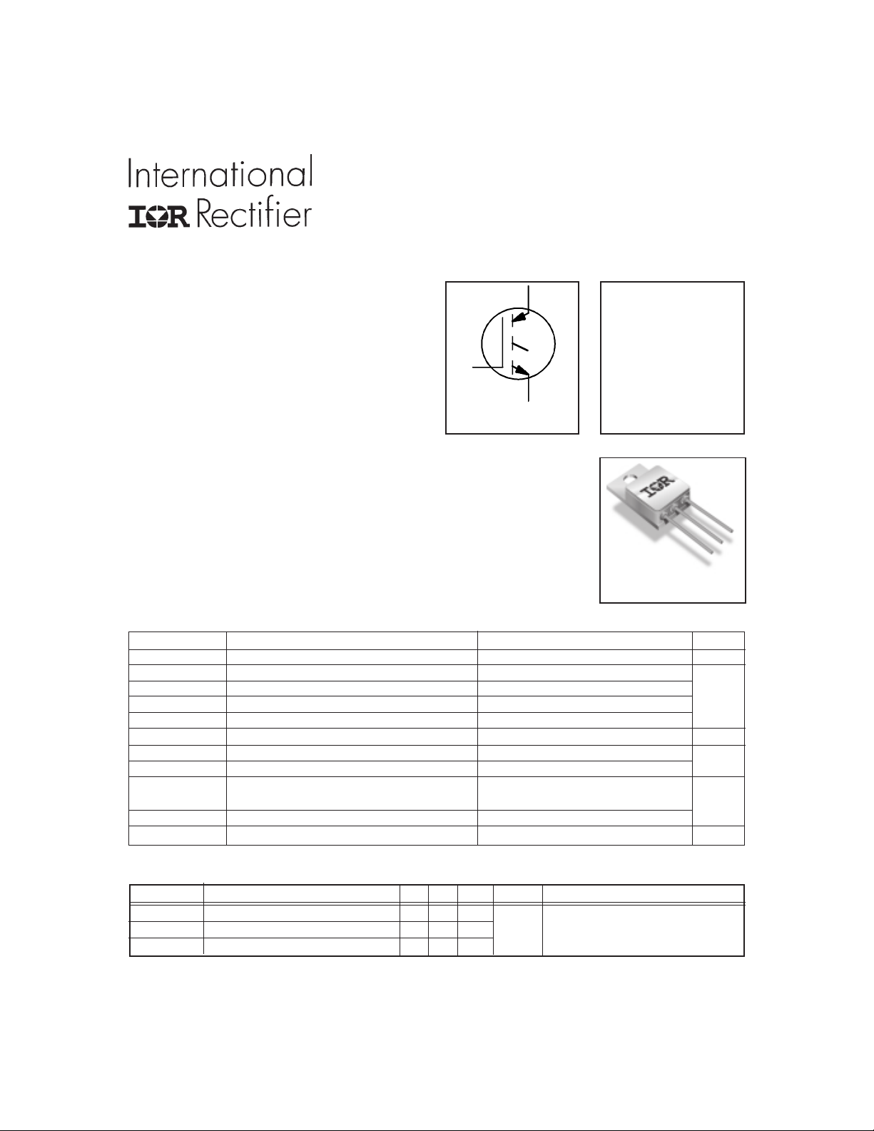
INSULATED GATE BIPOLAR TRANSISTOR
Features
C
Fast Speed IGBT
• Electrically Isolated and Hermetically Sealed
• Simple Drive Requirements
• Latch-proof
• Fast Speed operation 3 kHz - 8 kHz
• Switching-loss rating includes all "tail" losses
G
E
V
= 600V
CES
V
CE(on) max
= 1.7V
@VGE = 15V, IC = 30A
n-channel
Description
Insulated Gate Bipolar Transistors (IGBTs) from International Rectifier have
higher usable current densities than comparable bipolar transistors, while at the
same time having simpler gate-drive requirements of the familiar power MOSFET.
They provide substantial benefits to a host of high-voltage, high-current
applications.
The performance of various IGBTs varies greatly with frequency. Note that IR now
provides the designer with a speed benchmark (f
, or the "half-current frequency "),
Ic/2
as well as an indication of the current handling capability of the device.
TO-254AA
Absolute Maximum Ratings
Parameter Max. Units
V
CES
IC @ TC = 25°C Continuous Collector Current 35*
IC @ TC = 100°C Continuous Collector Current 30 A
I
CM
I
LM
V
GE
PD @ TC = 25°C Maximum Power Dissipation 150 W
PD @ TC = 100°C Maximum Power Dissipation 60
T
J
T
STG
*Current is limited by pin diameter
Collector-to-Emitter Breakdown Voltage 600 V
Pulsed Collector Current
Clamped Inductive Load Current
Gate-to-Emitter Voltage ± 20 V
Operating Junction and -55 to + 150
Storage Temperature Range °C
Lead Temperature 300 (0.063in./1.6mm from case for 10s)
Weight
➀➀
➀ 210
➀➀
➁➁
➁ 210
➁➁
9.3 (typical) g
Thermal Resistance
Parameter Min Typ Max Units Test Conditions
R
thJC
R
thCS
R
thJA
For footnotes refer to the last page
www.irf.com 1
Junction-to-Case — — 0.83
Case-to-Sink — 0.21 —
Junction-to-Ambient — — 48
°C/W
02/20/02
Page 2
IRGMC50F
Electrical Characteristics @ TJ = 25°C (unless otherwise specified)
Parameter Min. Typ. Max. Units Conditions
V
(BR)CES
V
(BR)ECS
∆V
(BR)CES
V
CE(ON)
V
GE(th)
∆V
GE(th)
g
fe
I
CES
I
GES
Switching Characteristics @ TJ = 25°C (unless otherwise specified)
Q
g
Q
ge
Q
gc
t
d(on)
t
r
t
d(off)
t
f
E
on
E
off
E
ts
t
d(on)
t
r
t
d(off)
t
f
E
ts
LC+L
E
C
ies
C
oes
C
res
Collector-to-Emitter Breakdown Voltage 600 ––– ––– V VGE = 0V, IC = 1.0 mA
Emitter-to-Collector Breakdown Voltage 15 ––– ––– V VGE = 0V, IC = 1.0 A
/∆T
Temperature Coeff. of Breakdown Voltage ––– 0.62 ––– V/°CVGE = 0V, IC = 1.0 mA
J
➂➂
➂
➂➂
––– ––– 1.7 IC = 30A VGE = 15V
Collector-to-Emitter Saturation Voltage ––– 2.0 ––– IC = 35A See Fig.5
––– 1.7 ––– IC = 30A , TJ = 125°C
V
Gate Threshold Voltage 3.0 ––– 5.5 VCE = VGE, IC = 250 µA
/∆TJTemperature Coeff. of Threshold Voltage ––– -14 ––– mV/°CVCE = VGE, IC = 250 µA
Forward Transconductance T 21 ––– ––– SVCE ≥ 15V, IC = 30A
Zero Gate Voltage Collector Current
––– ––– 50 VGE = 0V, VCE = 480V
––– ––– 2000 VGE = 0V, VCE = 480V, TJ = 125°C
µA
Gate-to-Emitter Leakage Current ––– ––– ±100 nA VGE = ±20V
Parameter Min. Typ. Max. Units Conditions
Total Gate Charge (turn-on) ––– 120 140 IC = 30A
Gate - Emitter Charge (turn-on) ––– 15 35 nC VCC = 300V See Fig. 8
Gate - Collector Charge (turn-on) ––– 35 70 VGE = 15V
Turn-On Delay Time ––– ––– 48 IC = 30A, VCC = 480V
Rise Time ––– ––– 100 VGE = 15V, RG = 2.35Ω
Turn-Off Delay Time ––– ––– 540 Energy losses include "tail"
ns
Fall Time ––– ––– 360 See Fig. 9, 10 & 13
Turn-On Switching Loss ––– 0.2 –––
Turn-off Switching Loss ––– 5.8 –––
mJ
Total Switching Loss ––– 6.0 10
Turn-On Delay Time ––– 25 ––– TJ = 125°C
Rise Time ––– 49 ––– IC = 30A, VCC = 480V
Turn-Off Delay Time ––– 440 ––– VGE = 15V, RG = 2.35Ω
ns
Fall Time ––– 410 ––– Energy losses include "tail"
Total Switching Loss ––– 10 ––– See Fig. 11, 13
mJ
Total Inductance ––– 6.8 ––– nH Measured from Collector lead (6mm/
0.25in. from package) to Emitter
lead (6mm / 0.25in. from package)
Input Capacitance ––– 3000 ––– VGE = 0V
Output Capacitance ––– 340 ––– pF VCC = 30V See Fig. 7
Reverse Transfer Capacitance ––– 40 ––– ƒ = 1.0MHz
Note: Corresponding Spice and Saber models are available on the Website.
For footnotes refer to the last page
2 www.irf.com
Page 3
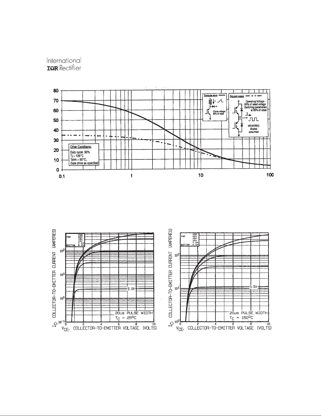
Fig. 1 - Typical Load Current vs. Frequency
(For square wave, I=I
of fundamental; for triangular wave, I=IPK)
RMS
IRGMC50F
Fig. 2 - Typical Output Characteristics
Fig. 3 - Typical Transfer Characteristics
www.irf.com 3
Page 4
IRGMC50F
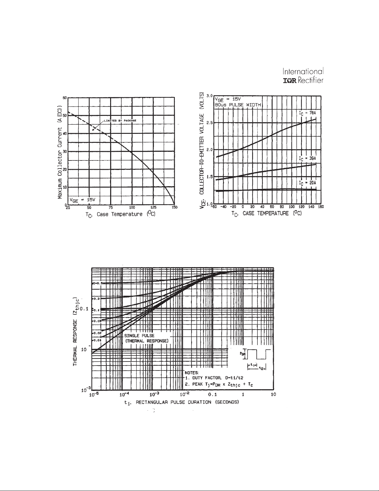
Fig. 4 - Maximum Collector Current vs. Case
Temperature
Fig. 6 - Maximum Effective Transient Thermal Impedance, Junction-to-Case
Fig. 5 - Collector-to-Emitter Voltage vs.
Junction Temperature
4 www.irf.com
Page 5
IRGMC50F
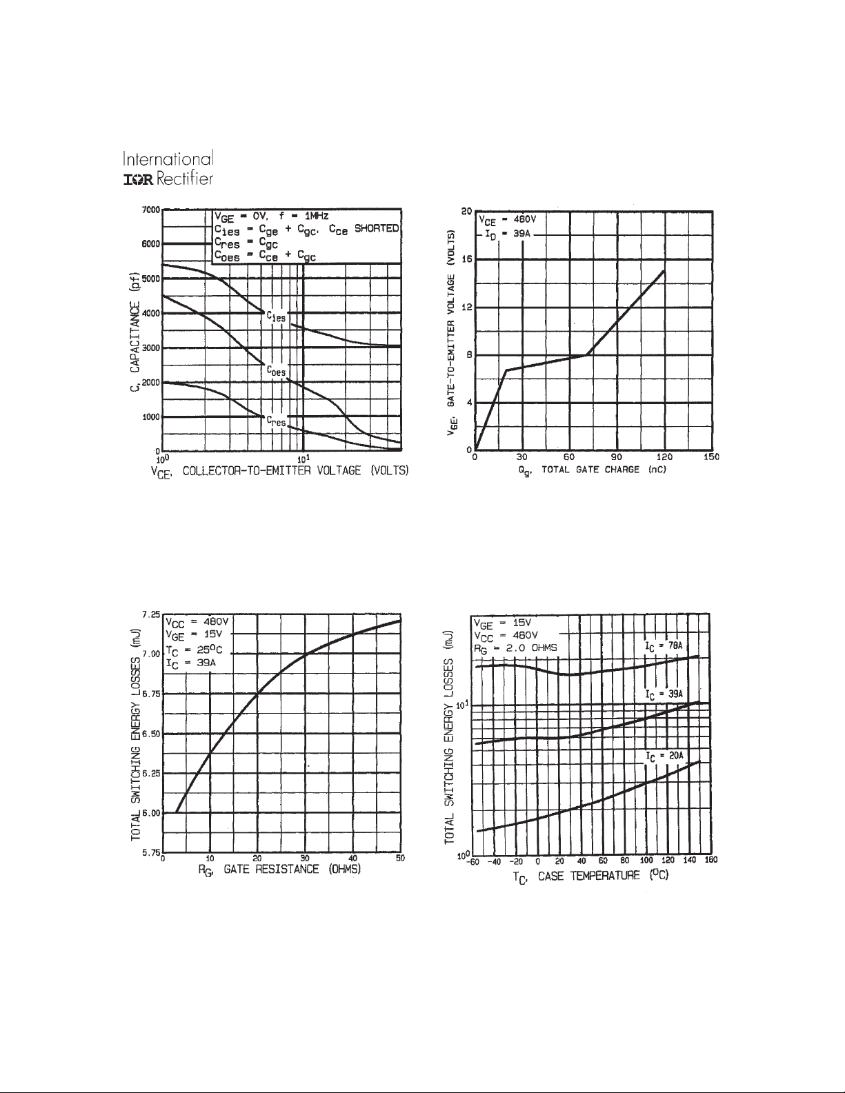
Fig. 7 - Typical Capacitance vs.
Collector-to-Emitter Voltage
Fig. 9 - Typical Switching Losses vs. Gate
Resistance
Fig. 8 - Typical Gate Charge vs.
Gate-to-Emitter Voltage
Fig. 10 - Typical Switching Losses vs.
Junction Temperature
www.irf.com 5
Page 6
IRGMC50F
125°C
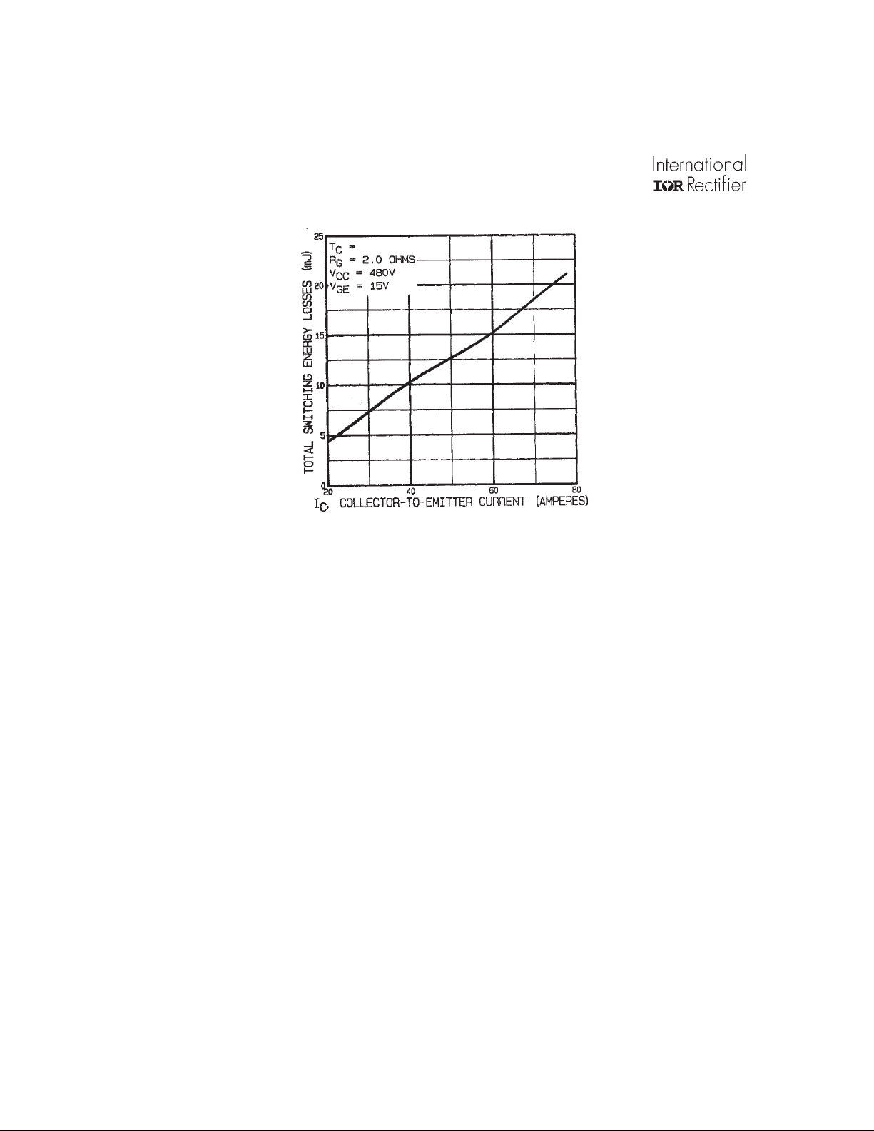
Fig. 11 - Typical Switching Losses vs.
Collector-to-Emitter Current
6 www.irf.com
Page 7
IRGMC50F
y
p
)
p
ply, p
50V
Q
* Driver same t
* Note: Due to the 50V power su
will in crease to ob tain rate d Id.
e as D.U.T.; Vc = 80% of Vce(max
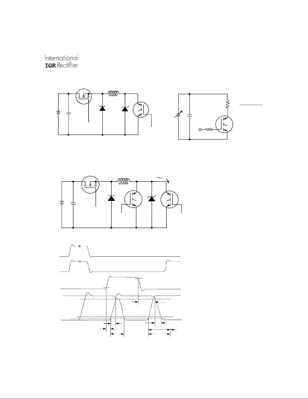
Fig. 12a - Clamped Inductive
Load Test Circuit
50V
1000V
Q
1000V
L
V *
C
ulse width and inductor
D.U.T.
L
Driver*
R
480V
RL =
X IC@25°C
0 - 480V
480µF
960V
4
R
Fig. 12b - Pulsed Collector
Current Test Circuit
I
C
V
C
S
D.U.T.
Fig. 13a - Switching Loss
Test Circuit
* Driver same type
as D.U.T., VC = 480V
Q
R
90%
S
V
C
90%
10%
5%
I
C
t
d(on)
10%
t
r
E
on
t
d(off)
E = (E +E )
ts on off
Fig. 13b - Switching Loss
Waveforms
t
f
E
off
t=5µ s
www.irf.com 7
Page 8
IRGMC50F
Notes:
Q Repetitive rating; V
= 20V, pulse width limited by
GE
max. junction temperature.
R V
= 80%(V
CC
CES
), V
= 20V, L = 10µH, RG = 10Ω
GE
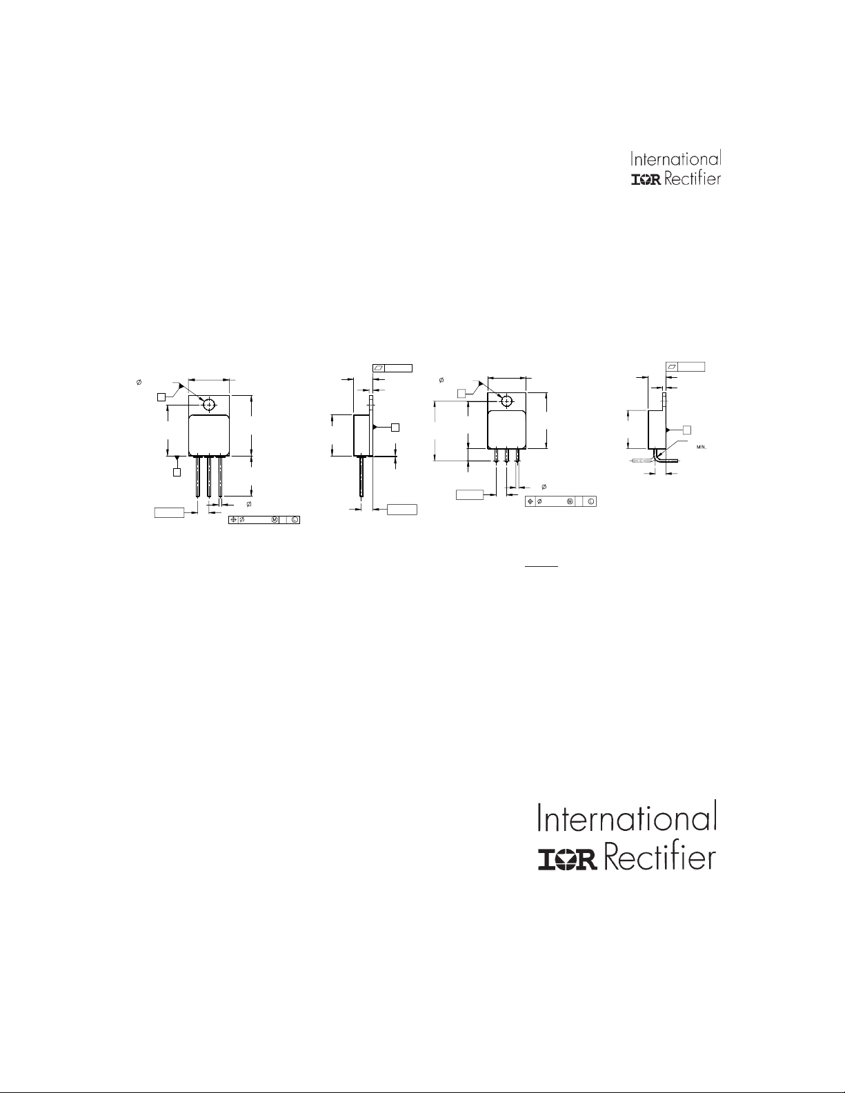
Case Outline and Dimensions — TO-254AA
3.78 [. 149]
3.53 [. 139]
17.40 [ .685]
16.89 [ .665]
3.81 [. 150]
13.84 [ .545]
13.59 [ .535]
A
20.32 [ .800]
20.07 [ .790]
123
C
2X
17.40 [ .685]
16.89 [ .665]
1.14 [.045]
3X
0.89 [.035]
0.36 [. 014]
6.60 [. 260]
6.32 [. 249]
13.84 [ .545]
13.59 [ .535]
B A
NOTE S:
1. DIMENS IONING & T OLERANCING PER ASME Y14.5M-1994.
2. AL L DI ME NS IONS ARE S HOWN IN MILL IMET ER S [ INCHES ].
3. CONTROLLING DIMENSION: INCH.
4. CONFORMS TO JEDEC OUTLINE TO-254AA.
0.12 [. 005]
1.27 [. 050]
1.02 [. 040]
B
0.84 [. 033]
MAX.
3.81 [. 150]
22.73 [.895]
21.21 [.835]
3.78 [.149]
3.53 [.139]
S Pulse width ≤ 80µs; duty factor ≤ 0.1%.
T Pulse width 5.0µs, single shot.
6.60 [.260]
6.32 [.249]
13.84 [.545]
13.59 [.535]
A
17.40 [.685]
16.89 [.665]
4.82 [.190]
3.81 [.150]
3.81 [.150]
2X
123
13.84 [.545]
13.59 [.535]
20.32 [.800]
20.07 [.790]
1.14 [.045]
3X
0.89 [.035]
0.36 [.014] B A
LEGEND
1 = COLLECTOR
2 = EMITTER
3 = GATE
0.12 [.005]
1.27 [.050]
1.02 [.040]
B
R 1.52 [.060]
4.06 [.160]
3.56 [.140]
BERYLLIA WARNING PER MIL-PRF-19500
CAUTION
Packages containing beryllia shall not be ground, sandblasted, machined or have other operations performed on them
which will produce beryllia or beryllium dust. Furthermore, beryllium oxide packages shall not be placed in acids that
will produce fumes containing beryllium.
IR WORLD HEADQUARTERS: 233 Kansas St., El Segundo, California 90245, USA Tel: (310) 252-7105
TAC Fax: (310) 252-7903
Visit us at www.irf.com for sales contact information.
Data and specifications subject to change without notice. 02/02
8 www.irf.com
 Loading...