

Page 1
PD - _____
PRELIMINARY
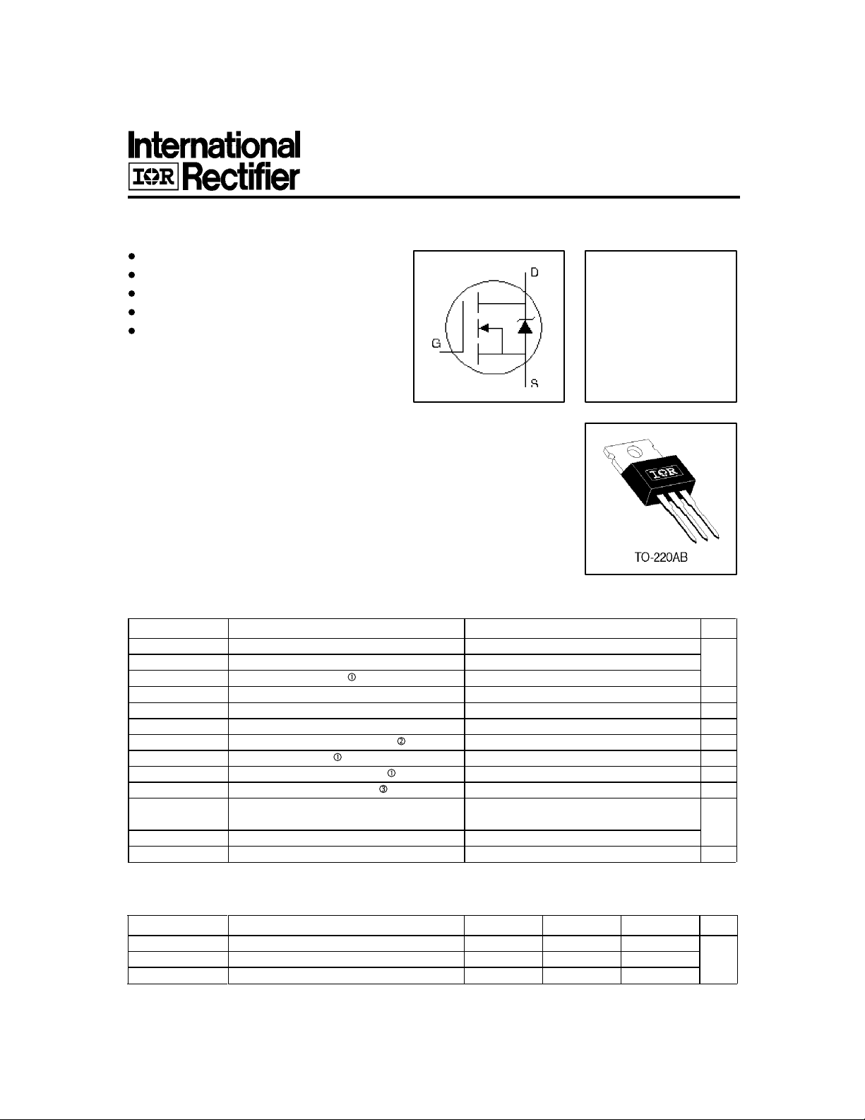
HEXFET® Power MOSFET
Advanced Process Technology
Dynamic dv/dt Rating
175°C Operating Temperature
Fast Switching
Fully Avalanche Rated
Description
Fifth Generation HEXFETs from International Rectifier utilize advanced processing
techniques to achieve the lowest possible on-resistance per silicon area. This
benefit, combined with the fast switching speed and ruggedized device design that
HEXFET Power MOSFETs are well known for, provides the designer with an
extremely efficient device for use in a wide variety of applications.
The TO-220 package is universally preferred for all commercial-industrial
applications at power dissipation levels to approximately 50 watts. The low
thermal resistance and low package cost of the TO-220 contribute to its wide
acceptance throughout the industry.
IRFZ34N
V
= 55V
DSS
R
DS(on)
ID = 26A
= 0.040Ω
Absolute Maximum Ratings
Parameter Max. Units
ID @ TC = 25°C Continuous Drain Current, VGS @ 10V 26
ID @ TC = 100°C Continuous Drain Current, VGS @ 10V 18 A
I
DM
PD @TC = 25°C Power Dissipation 56 W
V
GS
E
AS
I
AR
E
AR
dv/dt Peak Diode Recovery dv/dt 4.6 V/ns
T
J
T
STG
Pulsed Drain Current 100
Linear Derating Factor 0.37 W/°C
Gate-to-Source Voltage ±20 V
Single Pulse Avalanche Energy 110 mJ
Avalanche Current 16 A
Repetitive Avalanche Energy 5.6 mJ
Operating Junction and -55 to + 175
Storage Temperature Range °C
Soldering Temperature, for 10 seconds 300 (1.6mm from case)
Mounting torque, 6-32 or M3 screw. 10 lbf•in (1.1N•m)
Thermal Resistance
Parameter Min. Typ. Max. Units
R
θJC
R
θCS
R
θJA
Junction-to-Case –––– –––– 2.7
Case-to-Sink, Flat, Greased Surface –––– 0.50 –––– °C/W
Junction-to-Ambient –––– –––– 62
8/29/95
Page 2
IRFZ34N
Electrical Characteristics @ TJ = 25°C (unless otherwise specified)
Parameter Min. Typ. Max. Units Conditions
V
(BR)DSS
∆V
(BR)DSS
R
DS(ON)
V
GS(th)
g
fs
I
DSS
I
GSS
Q
g
Q
gs
Q
gd
t
d(on)
t
r
t
d(off)
t
f
L
D
L
S
C
iss
C
oss
C
rss
Drain-to-Source Breakdown Voltage 55 ––– ––– V VGS = 0V, ID = 250µA
/∆T
Breakdown Voltage Temp. Coefficient ––– 0.052 ––– V/°C Reference to 25°C, ID = 1mA
J
Static Drain-to-Source On-Resistance ––– ––– 0.040 Ω VGS = 10V, ID = 16A
Gate Threshold Voltage 2.0 ––– 4.0 V VDS = VGS, ID = 250µA
Forward Transconductance 6.5 ––– ––– S VDS = 25V, ID = 16A
Drain-to-Source Leakage Current
Gate-to-Source Forward Leakage ––– ––– 100 VGS = 20V
Gate-to-Source Reverse Leakage ––– ––– -100 VGS = -20V
––– ––– 25 VDS = 55V, VGS = 0V
––– ––– 250 VDS = 44V, VGS = 0V, TJ = 150°C
µA
nA
Total Gate Charge ––– ––– 34 ID = 16A
Gate-to-Source Charge ––– ––– 6.8 nC VDS = 44V
Gate-to-Drain ("Miller") Charge ––– ––– 14 VGS = 10V, See Fig. 6 and 13
Turn-On Delay Time ––– 7.0 ––– VDD = 28V
Rise Time ––– 49 ––– ID = 16A
Turn-Off Delay Time ––– 31 ––– RG = 18Ω
ns
Fall Time ––– 40 ––– RD = 1.8Ω, See Fig. 10
Internal Drain Inductance ––– 4.5 –––
Internal Source Inductance ––– 7.5 –––
Between lead,
6mm (0.25in.)
nH
from package
and center of die contact
Input Capacitance ––– 700 ––– VGS = 0V
Output Capacitance ––– 240 ––– pF VDS = 25V
Reverse Transfer Capacitance ––– 100 ––– ƒ = 1.0MHz, See Fig. 5
Source-Drain Ratings and Characteristics
Parameter Min. Typ. Max. Units Conditions
I
S
I
SM
V
SD
t
rr
Q
rr
t
on
Notes:
Repetitive rating; pulse width limited by
max. junction temperature. ( See fig. 11 )
V
DD
RG = 25Ω, I
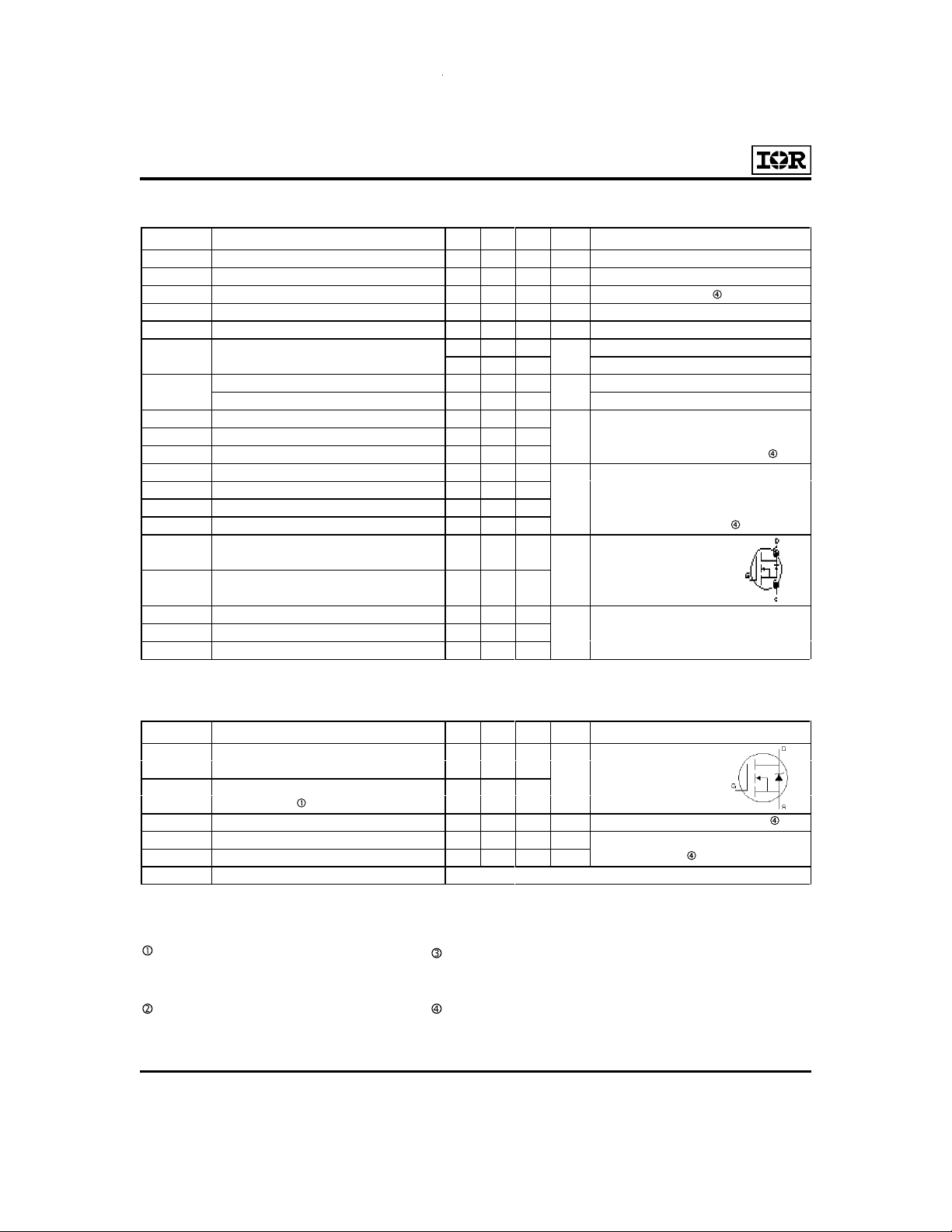
Continuous Source Current MOSFET symbol
(Body Diode) showing the
Pulsed Source Current integral reverse
(Body Diode) p-n junction diode.
––– ––– 26
––– ––– 100
Diode Forward Voltage ––– ––– 1.6 V TJ = 25°C, IS = 16A, VGS = 0V
Reverse Recovery Time ––– 57 86 ns TJ = 25°C, IF = 16A
Reverse Recovery Charge ––– 130 200 nC di/dt = 100A/µs
Forward Turn-On Time
Intrinsic turn-on time is negligible (turn-on is dominated by LS+LD)
I
SD
TJ ≤ 175°C
= 25V, starting TJ = 25°C, L = 610µH
= 16A. (See Figure 12)
AS
Pulse width ≤ 300µs; duty cycle ≤ 2%.
A
≤ 16 A, di/dt ≤ 420A/µs, V
DD
≤ V
(BR)DSS
,
Page 3
IRFZ34N
A
A
A
A
1000
VGS
TOP 15V
10V
8.0V
7.0V
6.0V
5.5V
5.0V
BOTTOM 4.5V
100
10
D
I , Drain-to-Source Current (A)
4.5V
20µs PULSE WIDTH
T = 25°C
1
0.1 1 10 100
V , Drain-to-Source Voltage (V)
DS
C
Fig 1. Typical Output Characteristics,
TC = 25oC
100
1000
VGS
TOP 15V
10V
8.0V
7.0V
6.0V
5.5V
5.0V
BOTTO M 4.5V
100
10
4.5V
D
I , Drain-to-Source Current (A)
20µs PULSE WIDTH
T = 175°C
1
0.1 1 10 100
V , Drain-to-Source Voltage (V)
DS
C
Fig 2. Typical Output Characteristics,
TC = 175oC
2.4
I = 26A
D
T = 25°C
J
T = 175°C
J
10
D
I , Drain-to-Source Current (A)
1
4 5 6 7 8 9 10
V , Gate-to-Source Voltage (V)
GS
V = 25V
DS
20µs PULSE WIDTH
2.0
1.6
1.2
(Normalized)
0.8
0.4
DS(on)
R , Drain-to-Source On Resistance
0.0
-60 -40 -20 0 20 40 60 80 100 120 140 160 180
T , Junction Temperature (°C)
J
Fig 3. Typical Transfer Characteristics Fig 4. Normalized On-Resistance
Vs. Temperature
V = 10V
GS
Page 4

IRFZ34N
A
A
A
A
1200
1000
800
600
400
C, Capacitance (pF)
200
0
1 10 100
V = 0V, f = 1MHz
GS
C = C + C , C SHORTED
iss gs gd ds
C = C
rss gd
C = C + C
C
oss ds gd
iss
C
oss
C
rss
V , Drain-to-Source Voltage (V)
DS
Fig 5. Typical Capacitance Vs.
Drain-to-Source Voltage
1000
20
I = 16A
D
16
12
8
4
GS
V , Gate-to-Source Voltage (V)
V = 44V
DS
V = 28V
DS
FOR TEST CIRCUIT
0
0 10 20 30 40
Q , Total Gate Charge (nC)
G
SEE FIGURE 13
Fig 6. Typical Gate Charge Vs.
Gate-to-Source Voltage
1000
OPERATION IN THIS AREA LIMITED
BY R
DS(on)
100
T = 175°C
J
T = 25°C
10
SD
I , Reverse Drain Current (A)
1
0.4 0.8 1.2 1.6 2.0
V , Source-to-Drain Voltage (V)
SD
J
V = 0V
Fig 7. Typical Source-Drain Diode
Forward Voltage
GS
100
10
D
I , Drain Current (A)
T = 25°C
C
T = 175°C
J
Single Pulse
1
1 10 100
V , Drain-to-Source Voltage (V)
DS
Fig 8. Maximum Safe Operating Area
10µs
100µs
1ms
10ms
Page 5

IRFZ34N
A
R
D.U.T.
D
V
DD
V
DS
V
30
25
GS
R
G
10 V
20
Pulse Width ≤ 1 µs
Duty Factor ≤ 0.1 %
15
10
D
I , Drain Current (Amps)
5
0
25 50 75 100 125 150 175
T , Case Temperature (°C)
C
Fig 9. Maximum Drain Current Vs.
Fig 10a. Switching Time Test Circuit
Fig 10b. Switching Time Waveforms
Case Temperature
10
thJC
D = 0.50
1
0.20
0.10
0.05
0.02
0.1
0.01
SINGLE PULSE
Thermal Response (Z )
0.01
0.00001 0.0001 0.001 0.01 0.1 1
(THERMAL RESPONSE)
N otes :
1. D uty fac tor D = t / t
2. P eak T = P x Z + T
t , Rectangular Pulse Duration (sec)
1
DM
J
1 2
thJC
P
D M
t
1
C
t
2
A
Fig 11. Maximum Effective Transient Thermal Impedance, Junction-to-Case
Page 6

IRFZ34N
A
10 V
Fig 12a. Unclamped Inductive Test Circuit
Fig 12b. Unclamped Inductive Waveforms
250
200
150
100
50
AS
V = 25V
E , Single Pulse Avalanche Energy (mJ)
DD
0
25 50 75 100 125 150 175
Starting T , Junction Temperature ( °C)
J
I
TOP 6.5A
11A
BOTTOM 16A
Fig 12c. Maximum Avalanche Energy
Vs. Drain Current
D
10 V
Fig 13a. Basic Gate Charge Waveform Fig 13b. Gate Charge Test Circuit
Appendix A: Figure 14, Peak Diode Recovery dv/dt Test Circuit
Appendix B: Package Outline Mechanical Drawing
Appendix C: Part Marking Information
Page 7

Appendix A
IRFZ34N
Peak Diode Recovery dv/dt Test Circuit
D.U.T
R
G
Circuit Layout Considerations
• Low Stray Inductance
• Ground Plane
• Low Leakage Inductance
Current Transformer
• dv/dt controlled by R
• Driver same type as D.U.T.
• ISD controlled by Duty Factor "D"
• D.U.T. - Device Under Test
G
V
DD
*
* VGS = 5V for Logic Level Devices
Fig 14. For N-Channel HEXFETS
Page 8

IRFZ34N
A
Package Outline
Appendix B
TO-220AB Outline
Dimensions are shown in millimeters (inches)
10.54 (.415)
2.87 (.113)
2.62 (.103)
15.24 (.600)
14.84 (.584)
14.09 (.555)
13.47 (.530)
1.40 (.055)
3X
1.15 (.045)
2.54 (.100)
NOTES:
1 DIMENSIONING & TOLERANCING PER ANSI Y14.5M, 1982. 3 OUTLINE CONFORMS TO JEDEC OUTLINE TO-220AB.
2 CONTROLLING DIMENSION : INCH 4 HEATSINK & LEAD MEASUREMENTS DO NOT INCLUDE BURRS.
2X
10.29 (.405)
4
1 2 3
3X
0.36 (.014) M B A M
6.47 (.255)
6.10 (.240)
1.15 (.045)
MIN
4.06 (.160)
3.55 (.140)
0.93 (.037)
0.69 (.027)
3.78 (.149)
3.54 (.139)
- A -
4.69 (.185)
4.20 (.165)
- B -
1.32 (.052)
1.22 (.048)
2.92 (.115)
2.64 (.104)
LEAD ASSIGNMENTS
1 - GATE
2 - DRAIN
3 - SOURCE
4 - DRAIN
0.55 (.022)
3X
0.46 (.018)
Part Marking Information
TO-220AB
EXAMPLE : THIS IS AN IRF1010
WITH ASSEMBLY
LOT CODE 9B1M
INTERNATIONAL
RECTIFIER
LOGO
ASSEMBLY
LOT CODE
IRF1010
9246
9B 1M
Appendix C
PART NUMBER
DATE CODE
(YYWW)
YY = YEAR
WW = WEEK
 Loading...