

Page 1
PD - 95055
IRFP4710PbF
HEXFET® Power MOSFET
Applications
l High frequency DC-DC converters
l Motor Control
l Uninterruptible Power Supplies
l Lead-Free
V
DSS
R
DS(on)
max I
100V 0.014Ω 72A
Benefits
l Low Gate-to-Drain Charge to Reduce
Switching Losses
l Fully Characterized Capacitance Including
Effective C
App. Note AN1001)
l Fully Characterized Avalanche Voltage
to Simplify Design, (See
OSS
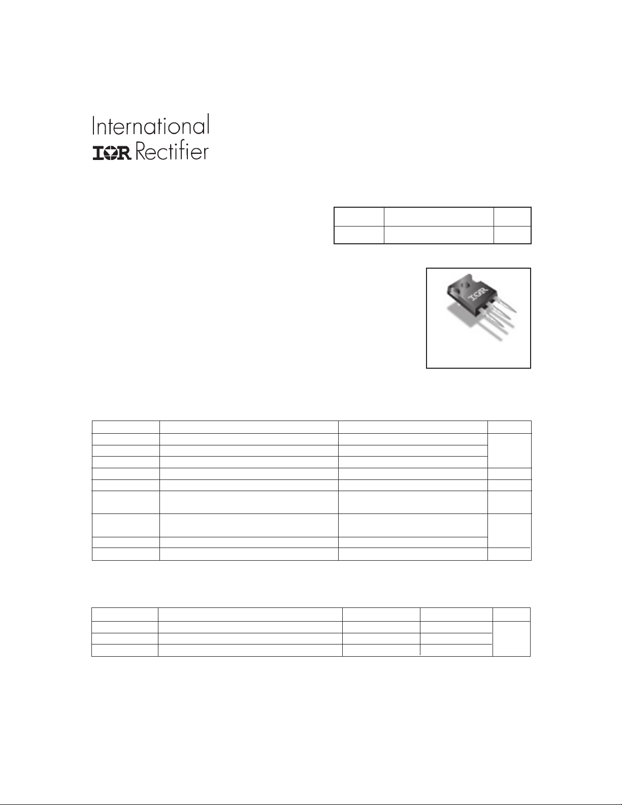
TO-247AC
and Current
Absolute Maximum Ratings
Parameter Max. Units
ID @ TC = 25°C Continuous Drain Current, VGS @ 10V 72
ID @ TC = 100°C Continuous Drain Current, VGS @ 10V 51 A
I
DM
PD @TC = 25°C Power Dissipation 190 W
V
GS
dv/dt Peak Diode Recovery dv/dt 8.2 V/ns
T
J
T
STG
Pulsed Drain Current 300
Linear Derating Factor 1.2 W/°C
Gate-to-Source Voltage ± 20 V
Operating Junction and -55 to + 175
Storage Temperature Range
Soldering Temperature, for 10 seconds 300 (1.6mm from case )
Mounting torqe, 6-32 or M3 screw 10 lbf•in (1.1N•m)
D
°C
Thermal Resistance
Parameter Typ. Max. Units
R
θJC
R
θCS
R
θJA
Notes through are on page 8
Junction-to-Case ––– 0.81
Case-to-Sink, Flat, Greased Surface 0.24 ––– °C/W
Junction-to-Ambient ––– 40
www.irf.com 1
2/26/04
Page 2
IRFP4710PbF
Static @ TJ = 25°C (unless otherwise specified)
Parameter Min. Typ. Max. Units Conditions
V
(BR)DSS
∆V
(BR)DSS
R
DS(on)
V
GS(th)
I
DSS
I
GSS
Dynamic @ TJ = 25°C (unless otherwise specified)
g
fs
Q
g
Q
gs
Q
gd
t
d(on)
t
r
t
d(off)
t
f
C
iss
C
oss
C
rss
C
oss
C
oss
C
eff. Effective Output Capacitance ––– 430 ––– VGS = 0V, VDS = 0V to 80V
oss
Drain-to-Source Breakdown Voltage 100 ––– ––– V VGS = 0V, ID = 250µA
/∆T
Breakdown Voltage Temp. Coefficient
J
––– 0.11 ––– V/°C Reference to 25°C, ID = 1mA
Static Drain-to-Source On-Resistance ––– 0.011 0.014 Ω VGS = 10V, ID = 45A
Gate Threshold Voltage 3.5 ––– 5.5 V VDS = VGS, ID = 250µA
Drain-to-Source Leakage Current
Gate-to-Source Forward Leakage ––– ––– 100 VGS = 20V
Gate-to-Source Reverse Leakage ––– ––– -100
––– ––– 1.0
––– ––– 250 VDS = 80V, VGS = 0V, TJ = 150°C
µA
nA
= 95V, VGS = 0V
V
DS
VGS = -20V
Parameter Min. Typ. Max. Units Conditions
Forward Transconductance 35 ––– ––– S VDS = 50V, ID = 45A
Total Gate Charge ––– 110 170 ID = 45A
Gate-to-Source Charge ––– 43 ––– nC VDS = 50V
Gate-to-Drain ("Miller") Charge ––– 40 ––– VGS = 10V,
Turn-On Delay Time ––– 35 ––– VDD = 50V
Rise Time ––– 130 ––– ID = 45A
Turn-Off Delay Time ––– 41 ––– RG = 4.5Ω
ns
Fall Time ––– 38 ––– VGS = 10V
Input Capacitance ––– 6160 ––– VGS = 0V
Output Capacitance ––– 440 ––– VDS = 25V
Reverse Transfer Capacitance ––– 250 ––– pF ƒ = 1.0MHz
Output Capacitance ––– 1580 ––– VGS = 0V, VDS = 1.0V, ƒ = 1.0MHz
Output Capacitance ––– 280 ––– VGS = 0V, VDS = 80V, ƒ = 1.0MHz
Avalanche Characteristics
Parameter Typ. Max. Units
E
AS
I
AR
E
AR
Single Pulse Avalanche Energy ––– 190 mJ
Avalanche Current ––– 45 A
Repetitive Avalanche Energy ––– 20 mJ
Diode Characteristics
Parameter Min. Typ. Max. Units Conditions
I
S
I
SM
V
SD
t
rr
Q
rr
t
on
Continuous Source Current MOSFET symbol
(Body Diode)
Pulsed Source Current integral reverse
(Body Diode)
––– –––
––– –––
72
300
showing the
A
p-n junction diode.
G
Diode Forward Voltage ––– ––– 1.3 V TJ = 25°C, IS = 45A, VGS = 0V
Reverse Recovery Time ––– 74 110 ns TJ = 25°C, IF = 45A
Reverse RecoveryCharge ––– 180 260 nC di/dt = 100A/µs
Forward Turn-On Time Intrinsic turn-on time is negligible (turn-on is dominated by LS+LD)
2 www.irf.com
D
S
Page 3
IRFP4710PbF
1000
100
10
1
0.1
D
I , Drain-to-Source Current (A)
TOP
BOTTOM
VGS
15V
12V
10V
8.0V
7.5V
7.0V
6.5V
6.0V
6.0V
20µs PULSE WIDTH
T = 25 C
0.01
0.1 1 10 100
V , Drain-to-Source Voltage (V)
DS
1000
J
1000
100
10
D
I , Drain-to-Source Current (A)
°
1
0.1 1 10 100
VGS
TOP
15V
12V
10V
8.0V
7.5V
7.0V
6.5V
BOTTOM
6.0V
6.0V
20µs PULSE WIDTH
T = 175 C
J
V , Drain-to-Source Voltage (V)
DS
°
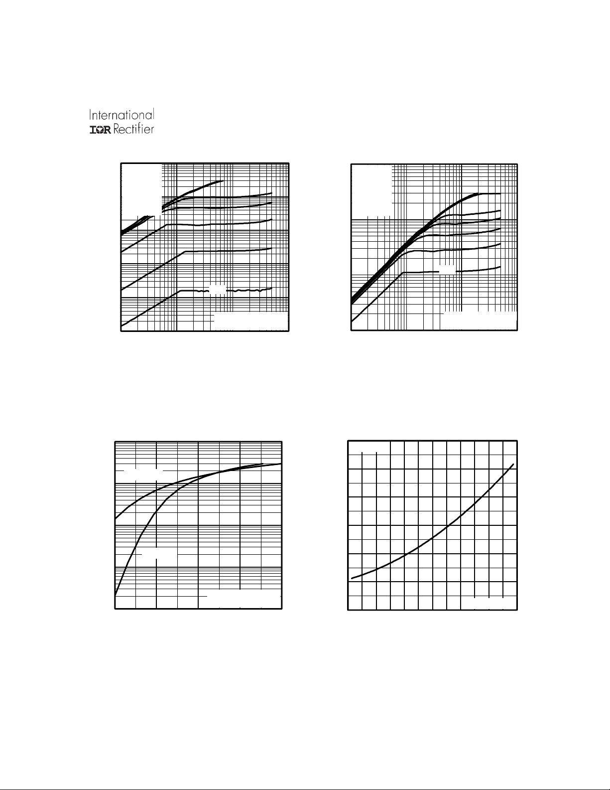
Fig 2. Typical Output CharacteristicsFig 1. Typical Output Characteristics
3.0
I =
D
75A
°
T = 175 C
100
D
I , Drain-to-Source Current (A)
J
10
°
T = 25 C
J
1
V = 50V
DS
0.1
6.0 7.0 8.0 9.0 10.0
V , Gate-to-Source Voltage (V)
GS
20µs PULSE WIDTH
Fig 3. Typical Transfer Characteristics
2.5
2.0
1.5
(Normalized)
1.0
0.5
DS(on)
R , Drain-to-Source On Resistance
0.0
-60 -40 -20 0 20 40 60 80 100 120 140 160 180
T , Junction Temperature ( C)
J
Fig 4. Normalized On-Resistance
V =
GS
°
10V
Vs. Temperature
www.irf.com 3
Page 4
IRFP4710PbF
10000
8000
)
F
p
(
e
6000
c
n
a
t
i
c
a
p
4000
a
C
,
C
2000
Ciss
V
= 0V, f = 1 MHZ
GS
C
= C
iss
gs
C
= C
rss
gd
C
= C
ds
+ C
oss
+ Cgd, C
gd
ds
Coss
Crss
0
1 10 100
VDS, Drain-to-Source Voltage (V)
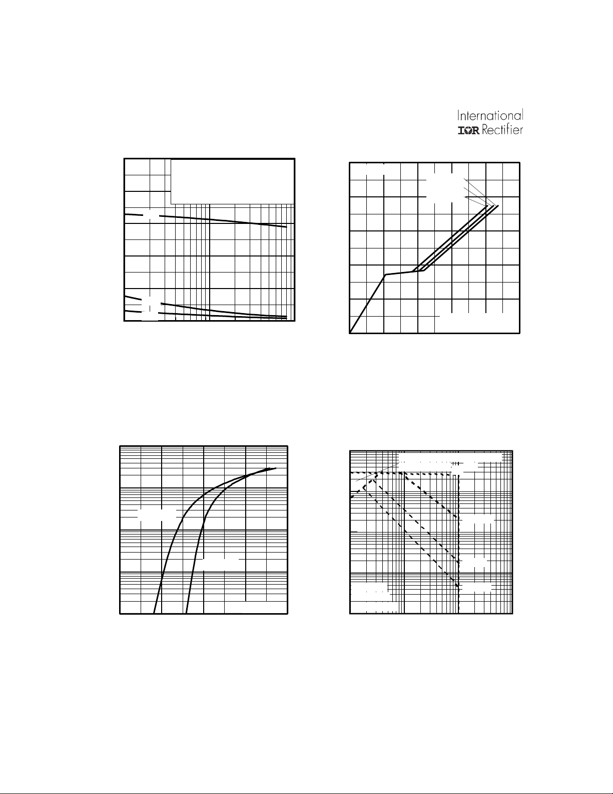
Fig 5. Typical Capacitance Vs.
Drain-to-Source Voltage
1000
100
°
T = 175 C
J
10
°
T = 25 C
1
SD
I , Reverse Drain Current (A)
0.1
0.0 0.4 0.8 1.2 1.6
V ,Source-to-Drain Voltage (V)
SD
J
V = 0 V
SHORTED
GS
20
I =
45A
16
12
8
4
GS
V , Gate-to-Source Voltage (V)
D
V = 80V
DS
V = 50V
DS
V = 20V
DS
FOR TEST CIRCUIT
0
0 40 80 120 160 200
Q , Total Gate Charge (nC)
G
SEE FIGURE
Fig 6. Typical Gate Charge Vs.
Gate-to-Source Voltage
1000
)
A
(
t
100
n
e
r
r
u
C
e
c
r
10
u
o
S
o
t
n
i
a
r
1
D
,
D
Tc = 25°C
I
Tj = 175°C
Single Pulse
0.1
1 10 100 1000
OPERATION IN THIS AREA
LIMITED BY RDS(on)
V
, Drain-toSource Voltage (V)
DS
100µsec
1msec
10msec
13
Fig 7. Typical Source-Drain Diode
Fig 8. Maximum Safe Operating Area
Forward Voltage
4 www.irf.com
Page 5
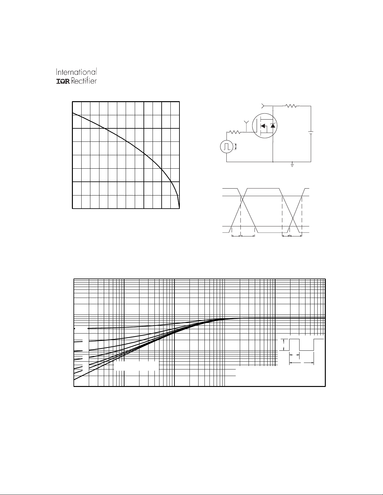
IRFP4710PbF
R
D.U.T.
D
+
V
DD
-
80
60
R
V
DS
V
GS
G
10V
40
Pulse Width ≤ 1 µs
Duty Factor ≤ 0.1 %
D
I , Drain Current (A)
20
Fig 10a. Switching Time Test Circuit
V
DS
90%
0
25 50 75 100 125 150 175
T , Case Temperature ( C)
C
Fig 9. Maximum Drain Current Vs.
°
10%
V
GS
t
d(on)tr
t
d(off)tf
Case Temperature
Fig 10b. Switching Time Waveforms
10
thJC
1
D = 0.50
0.20
0.10
0.1
0.05
Thermal Response (Z )
0.02
0.01
0.01
0.00001 0.0001 0.001 0.01 0.1 1
SINGLE PULSE
(THERMAL RESPONSE)
t , Rectangular Pulse Duration (sec)
1
Not es:
1. Duty factor D = t / t
2. Peak T = P x Z + T
J DM thJC C
1 2
P
DM
t
1
t
2
Fig 11. Maximum Effective Transient Thermal Impedance, Junction-to-Case
www.irf.com 5
Page 6
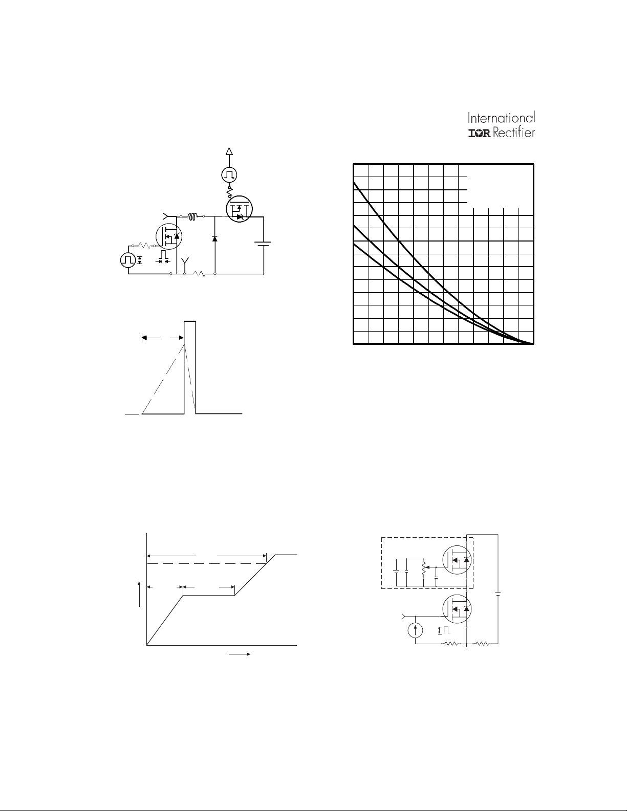
IRFP4710PbF
A
15V
V
DS
R
G
V
20V
GS
L
D.U.T
I
AS
Ω
0.01
t
p
DRIVER
+
V
DD
-
Fig 12a. Unclamped Inductive Test Circuit
V
(BR)DSS
t
p
I
AS
Fig 12b. Unclamped Inductive Waveforms
350
300
TOP
BOTTOM
250
200
150
100
50
AS
E , Single Pulse Avalanche Energy (mJ)
0
25 50 75 100 125 150 175
Starting T , Junction Temperature ( C)
J
Fig 12c. Maximum Avalanche Energy
Vs. Drain Current
I
°
D
18A
32A
45A
Current Regulator
Same Type as D.U.T.
Q
G
10 V
Q
GS
V
G
Q
GD
Charge
Fig 13a. Basic Gate Charge Waveform
12V
V
GS
Fig 13b. Gate Charge Test Circuit
50KΩ
.2µF
.3µF
3mA
Current Sampling Resistors
+
V
D.U.T.
I
G
DS
-
I
D
6 www.irf.com
Page 7
IRFP4710PbF
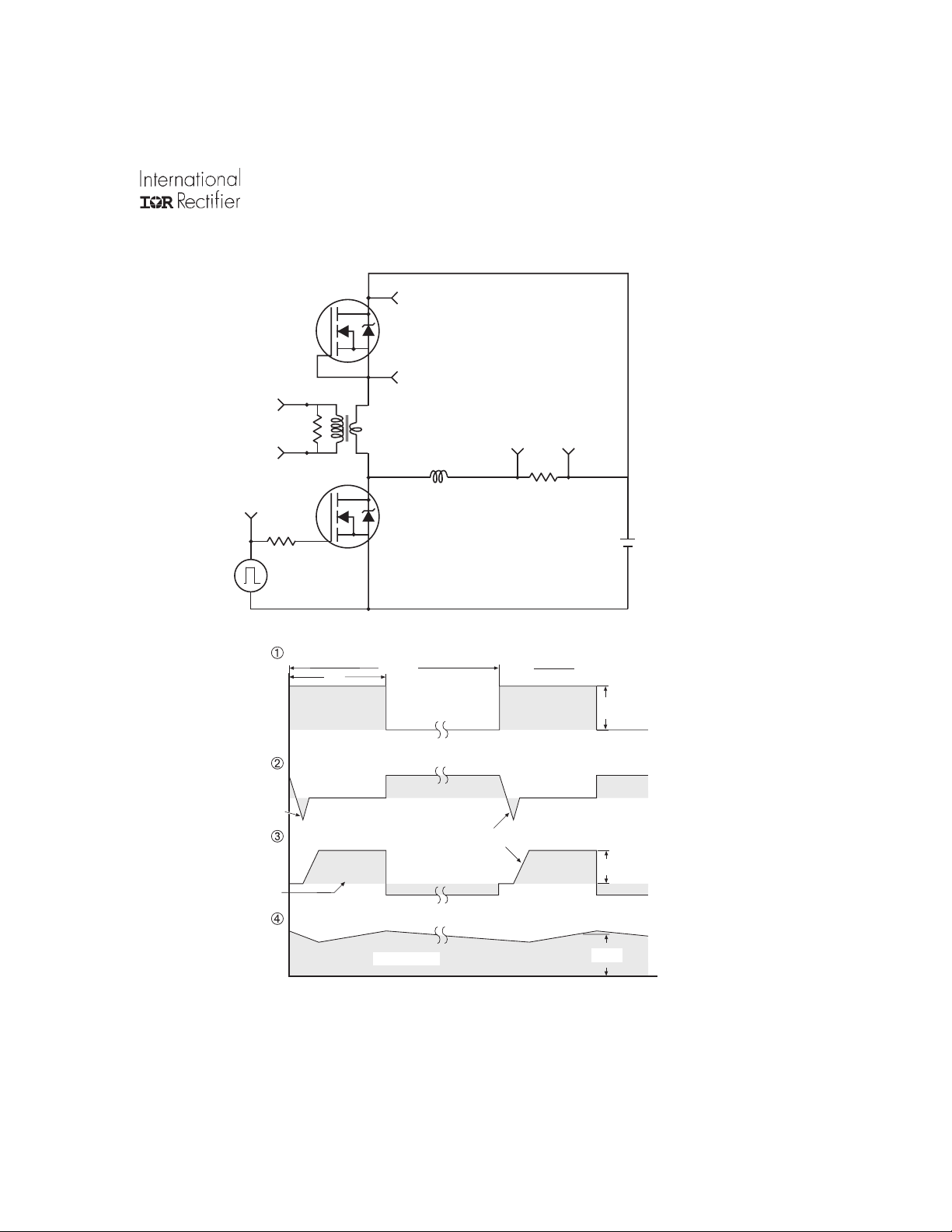
Peak Diode Recovery dv/dt Test Circuit
+
D.U.T
-
R
G
Driver Gate Drive
P.W.
+
Circuit Layout Considerations
• Low Stray Inductance
• Ground Plane
• Low Leakage Inductance
Current Transformer
-
-
• dv/dt controlled by R
• Driver same type as D.U.T.
G
• ISD controlled by Duty Factor "D"
• D.U.T. - Device Under Test
Period
D =
Period
P. W .
+
+
V
DD
-
VGS=10V
*
D.U.T. ISDWaveform
Reverse
Recovery
Current
Re-Applied
Voltage
D.U.T. VDSWaveform
Inductor Curent
* V
= 5V for Logic Level Devices
GS
Body Diode Forward
Current
di/dt
Diode Recovery
dv/dt
Body Diode Forward Drop
Ripple ≤ 5%
V
DD
I
SD
Fig 14. For N-Channel HEXFET® Power MOSFETs
www.irf.com 7
Page 8
IRFP4710PbF
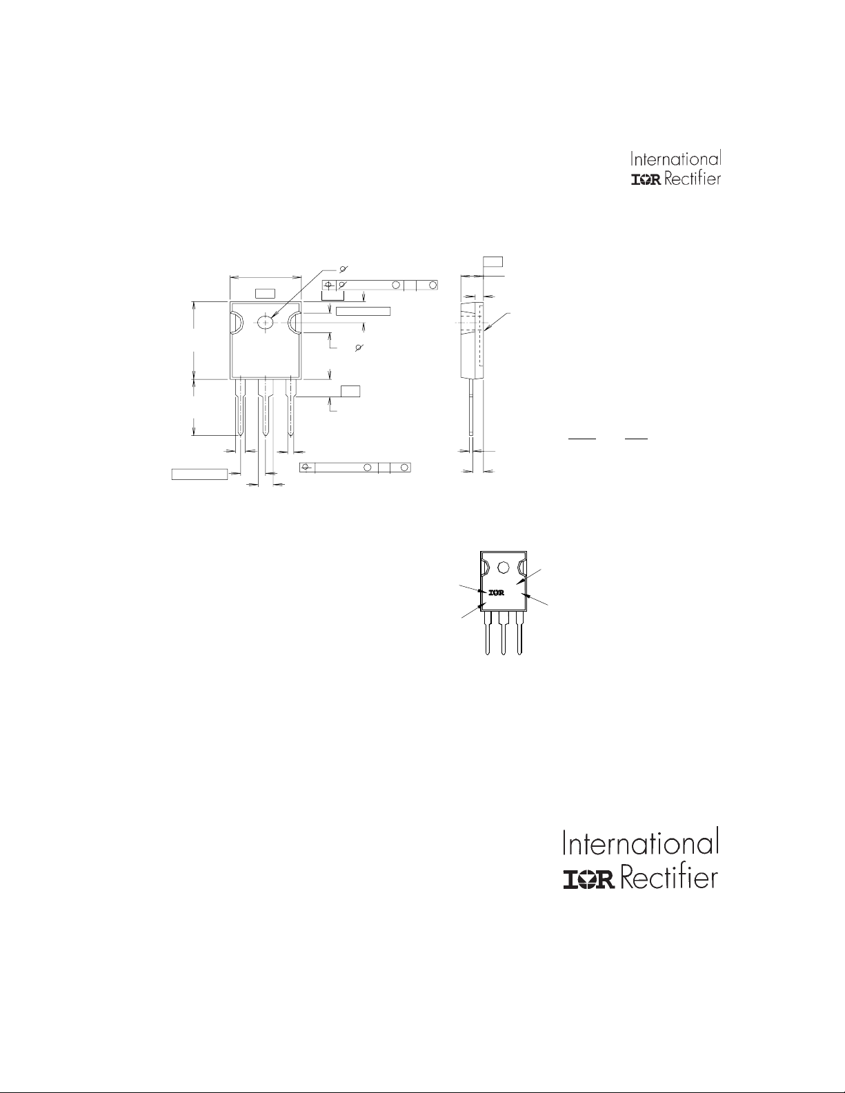
TO-247AC Package Outline
Dimensions are shown in millimeters (inches)
- A -
5.50 (.217)
2X
- C -
4.30 (.170)
3.70 (.145)
1.40 (.056)
1.00 (.039)
0.25 (.010)
3.65 (.143)
3.55 (.140)
0.25 (.010)
5.50 (.217)
4.50 (.177)
M
C
D
MMB
A
S
20.30 (. 800)
19.70 (. 775)
14.80 (.583)
14.20 (.559)
2.40 (.094)
2.00 (.079)
2X
5.45 (.215)
2X
15.90 (.626)
15.30 (.602)
- B -
123
3.40 (.133)
3.00 (.118)
3X
TO-247AC Part Marking Information
EXAMPLE:
THIS IS AN IRF PE30
WITH ASSEMBLY
LOT CODE 5657
ASS EMB LED ON WW 35, 2000
IN THE AS SEMBLY LINE "H"
Note: "P" in assembly line
positio n indicates "L ead-Free"
INTER NATIONAL
RECTIF IER
LOGO
ASSEMBLY
LOT CODE
- D -
2.50 (.089)
1.50 (.059)
3X
2.60 (.102)
2.20 (.087)
IRFPE30
56 57
5.30 (.209)
4.70 (.185)
4
NOTES:
1 DIMENSIONING & TOLERANCING
PER ANSI Y14.5M, 1982.
2 CONTROLLING DIMENSION : INCH.
3 CONFORMS TO JEDEC OUTLINE
TO-247-AC.
LEAD ASSIGNMENTS
Hexfet
0.80 (.031)
0.40 (.016)
035H
LEAD ASSIGNMENTS
1 - Gate
2 - Drain
3 - Source
4 - Drain
PART NUMBER
DAT E CODE
YEAR 0 = 2000
WE EK 35
LINE H
1 - GATE
2 - DRAIN
3 - SOURCE
4 - DRAIN
IGBT
1 - Gate
2 - Coll ector
3 - Emitter
4 - Coll ector
Notes:
Repetitive rating; pulse width limited by
max. junction temperature.
Starting T
RG = 25Ω, I
I
SD
= 25°C, L = 190µH
J
= 45A, VGS = 10V.
AS
≤ 45A, di/dt ≤ 420A/µs, V
DD
≤ V
TJ ≤ 175°C .
(BR)DSS
Pulse width ≤ 400µs; duty cycle ≤ 2%.
C
eff. is a fixed capacitance that gives the same charging
oss
time as C
oss
while V
DS
,
Data and specifications subject to change without notice.
is rising from 0 to 80% V
DSS
.
This product has been designed and qualified for the Industrial market.
Qualification Standards can be found on IR’s Web site.
IR WORLD HEADQUARTERS: 233 Kansas St., El Segundo, California 90245, USA Tel: (310) 252-7105
TAC Fax: (310) 252-7903
Visit us at www.irf.com for sales contact information. 02/04
8 www.irf.com
Page 9

Note: For the most current drawings please refer to the IR website at:
http://www.irf.com/package/
 Loading...