

Page 1
PD-93946A
IRFP460P
l Dynamic dv/dt Rating
l Repetitive Avalanche Rated
l Isolated Central Mounting Hole
l Fast Switching
l Ease of Paralleling
l Simple Drive Requirements
l Solder Plated for Reflowing
Description
Third Generation HEXFET®s from International Rectifier
G
HEXFET® Power MOSFET
D
V
= 500V
DSS
R
DS(on)
= 0.27Ω
ID = 20A
S
provide the designer with the best combination of fast
switching, ruggedized device design, low on-resistance
and cost-effectiveness.
The TO-247 package is preferred for commercial-industrial
applications where higher power levels preclude the use
of TO-220 devices. The TO-247 is similar but superior to
the earlier TO-218 package because of its isolated
mounting hole. It also provides greater creepage distance
between pins to meet the requirements of most safety
specifications.
The solder plated version of the TO-247 allows the reflow
TO-247AC
soldering of the package heatsink to a substrate material.
Absolute Maximum Ratings
Parameter Max. Units
ID @ TC = 25°C Continuous Drain Current, VGS @ 10V 20
ID @ TC = 100°C Continuous Drain Current, VGS @ 10V 13 A
I
DM
PD @TC = 25°C Power Dissipation 280 W
V
GS
E
AS
I
AR
E
AR
dv/dt Peak Diode Recovery dv/dt 3.5 V/ns
T
J
T
STG
Maximum Reflow Temperature 230 (Time above 183 °C
should not exceed 100s) °C
Pulsed Drain Current 80
Linear Derating Factor 2.2 W/°C
Gate-to-Source Voltage ± 20 V
Single Pulse Avalanche Energy 960 mJ
Avalanche Current 20 A
Repetitive Avalanche Energy 28 mJ
Operating Junction and -55 to + 150
Storage Temperature Range
Soldering Temperature, for 10 seconds 300 (1.6mm from case )
Mounting torque, 6-32 or M3 srew 10 lbf•in (1.1N•m)
°C
Thermal Resistance
Parameter Typ. Max. Units
R
θJC
R
θCS
R
θJA
Junction-to-Case ––– 0.45
Case-to-Sink, Flat, Greased Surface 0.24 ––– °C/W
Junction-to-Ambient ––– 40
www.irf.com 1
01/17/01
Page 2
IRFP460P
Electrical Characteristics @ TJ = 25°C (unless otherwise specified)
Parameter Min. Typ. Max. Units Conditions
V
(BR)DSS
∆V
(BR)DSS
R
DS(on)
V
GS(th)
g
fs
I
DSS
I
GSS
Q
g
Q
gs
Q
gd
t
d(on)
t
r
t
d(off)
t
f
L
D
L
S
C
iss
C
oss
C
rss
Drain-to-Source Breakdown Voltage 500 ––– ––– VVGS = 0V, ID = 250µA
/∆T
Breakdown Voltage Temp. Coefficient ––– 0.63 ––– V/°C Reference to 25°C, ID = 1mA
J
Static Drain-to-Source On-Resistance ––– ––– 0.27 Ω VGS = 10V, ID = 12A
Gate Threshold Voltage 2.0 ––– 4.0 V VDS = VGS, ID = 250µA
Forward Transconductance 13 ––– ––– SVDS = 50V, ID =12A
Drain-to-Source Leakage Current
––– ––– 25
––– ––– 250 VDS = 400V, VGS = 0V, TJ = 125°C
Gate-to-Source Forward Leakage ––– ––– 100 VGS = 20V
Gate-to-Source Reverse Leakage ––– ––– -100
VDS = 500V, VGS = 0V
µA
nA
VGS =-20V
Total Gate Charge ––– ––– 210 ID = 20A
Gate-to-Source Charge ––– ––– 29 nC VDS = 400V
Gate-to-Drain ("Miller") Charge ––– ––– 110 VGS = 10V, See Fig. 6 and 13
Turn-On Delay Time ––– 18 ––– VDD = 250V
Rise Time ––– 59 ––– ID = 20A
Turn-Off Delay Time ––– 110 ––– RG = 4.3Ω
ns
Fall Time ––– 58 ––– RD = 13Ω,See Fig. 10
5.0
Internal Drain Inductance
Internal Source Inductance ––– –––
––– –––
13
Between lead,
6mm (0.25in.)
nH
from package
and center of die contact
Input Capacitance ––– 4200 ––– VGS = 0V
Output Capacitance ––– 870 ––– VDS = 25V
Reverse Transfer Capacitance ––– 350 ––– pF ƒ = 1.0MHz, See Fig. 5
D
G
S
Source-Drain Ratings and Characteristics
Parameter Min. Typ. Max. Units Conditions
I
S
I
SM
V
SD
t
rr
Q
rr
t
on
Continuous Source Current MOSFET symbol
(Body Diode)
Pulsed Source Current integral reverse
(Body Diode)
––– –––
––– –––
20
80
showing the
A
p-n junction diode.
G
Diode Forward Voltage ––– ––– 1.8 V TJ = 25°C, IS = 20A, VGS = 0V
Reverse Recovery Time ––– 570 860 ns TJ = 25°C, IF = 20A
Reverse RecoverCharge ––– 5.7 8.6 µC di/dt = 100A/µs
Forward Turn-On Time Intrinsic turn-on time is negligible (turn-on is dominated by LS+LD)
Notes:
Repetitive rating; pulse width limited by
max. junction temperature. ( See fig. 11 )
Starting T
RG = 25Ω, I
= 25°C, L =4.8mH
J
= 20A. (See Figure 12)
AS
I
≤ 20A, di/dt ≤ 160A/µs, V
SD
DD
≤ V
(BR)DSS
TJ ≤ 150°C
Pulse width ≤ 300µs; duty cycle ≤ 2%.
,
2 www.irf.com
D
S
Page 3
IRFP460P
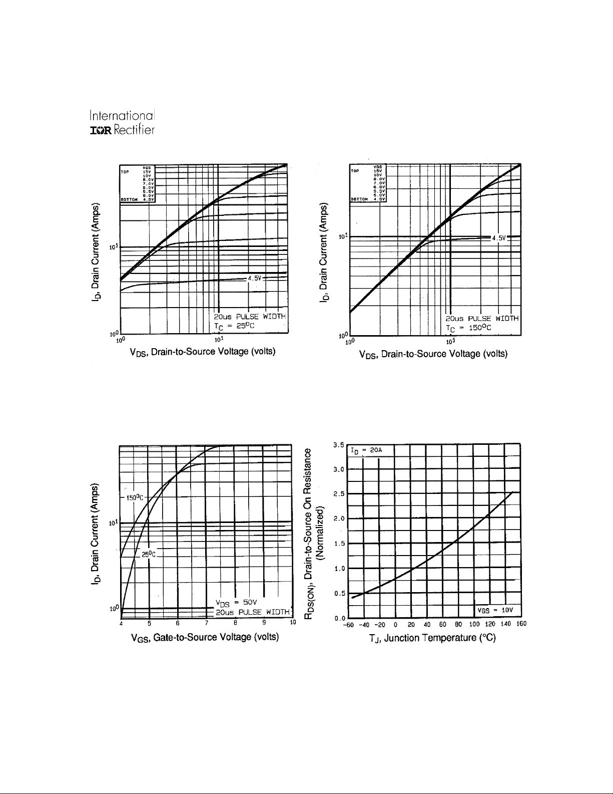
Fig 1. Typical Output Characteristics
Fig 3. Typical Transfer Characteristics Fig 4. Normalized On-Resistance
www.irf.com 3
Fig 2. Typical Output Characteristics
Vs. Temperature
Page 4

IRFP460P
Fig 5. Typical Capacitance Vs.
Drain-to-Source Voltage
Fig 7. Typical Source-Drain Diode
Forward Voltage
4 www.irf.com
Fig 6. Typical Gate Charge Vs.
Gate-to-Source Voltage
Fig 8. Maximum Safe Operating Area
Page 5

Fig 9. Maximum Drain Current Vs.
Case Temperature
IRFP460P
R
D.U.T.
t
d(off)tf
D
V
DS
V
GS
R
G
10V
Pulse Width ≤ 1 µs
Duty Factor ≤ 0.1 %
Fig 10a. Switching Time Test Circuit
V
DS
90%
10%
V
GS
t
d(on)tr
Fig 10b. Switching Time Waveforms
+
V
DD
-
Fig 11. Maximum Effective Transient Thermal Impedance, Junction-to-Case
www.irf.com 5
Page 6

IRFP460P
A
15V
DRIVER
+
-
V
DD
R
20V
V
DS
G
t
L
D.U.T
I
AS
0.01
p
Ω
Fig 12a. Unclamped Inductive Test Circuit
V
(BR)DSS
t
p
I
AS
Fig 12b. Unclamped Inductive Waveforms
Fig 12c. Maximum Avalanche Energy
Vs. Drain Current
Current Regulator
Same Type as D.U.T.
Q
10 V
G
12V
Q
GS
V
G
Q
GD
V
GS
Charge
50KΩ
.2µF
.3µF
3mA
Current Sampling Resistors
+
V
D.U.T.
I
G
DS
-
I
D
Fig 13b. Gate Charge Test CircuitFig 13a. Basic Gate Charge Waveform
6 www.irf.com
Page 7

IRFP460P
Peak Diode Recovery dv/dt Test Circuit
+
D.U.T
-
R
G
Driver Gate Drive
P.W.
+
Circuit Layout Considerations
• Low Stray Inductance
• Ground Plane
• Low Leakage Inductance
Current Transformer
-
-
• dv/dt controlled by R
• Driver same type as D.U.T.
G
• ISD controlled by Duty Factor "D"
• D.U.T. - Device Under Test
Period
D =
Period
P.W.
+
+
V
DD
-
VGS=10V
*
D.U.T. ISDWaveform
Reverse
Recovery
Current
Re-Applied
Voltage
D.U.T. VDSWaveform
Inductor Curent
* V
= 5V for Logic Level Devices
GS
Body Diode Forward
Current
di/dt
Diode Recovery
dv/dt
Body Diode Forward Drop
Ripple ≤ 5%
V
DD
I
SD
Fig 14. For N-Channel HEXFET®s
www.irf.com 7
Page 8

IRFP460P
(
)
)
)
)
(
)
)
)
)
)
)
(
)
(
)
)
(
)
)
)
)
)
)
)
)
)
)
(
)
)
)
)
)
)
(
)
A
Package Outline
TO-247AC
Dimensions are shown in millimeters (inches)
- A -
2X
4.30
3.70 (.145
3.65 (.143
3.55 (.140
0.25 (.010
5.50 (.217
- C .170
20.30
.800
19.70 (.775
14.80 (.583
14.20 (.559
15.90 (.6 2 6
15.30 (.6 0 2
- B -
12
3
MMB
.2 1 7
5.50
4.50 (.1 7 7
- D -
5.30
.209
D
4.70 (.185
2.50 (.089
1.50 (.059
4
NOTES:
1 DIMENSIONING & TOLERANCING
PER ANSI Y14.5M, 1982.
2 CONTROLLING DIMENSION : INCH.
3 CONFORMS TO JEDEC OUTLINE
TO -2 4 7 -AC.
2.40 (.094
2.00 (.079
2X
5.45
.215
2X
3X
3.40 (.1 3 3
3.00 (.1 1 8
1.40 (.056
1.00 (.039
0.25
Part Marking Information
TO-247AC
EXAMPLE : THIS IS AN IRFPE30
W ITH ASSEMBLY
L O T CO D E 3 A1 Q
This product has been designed and qualified for the industrial market.
.010
M
INTE RN A TION AL
R E CT IF IE R
L O G O
ASSEMBLY
LO T C ODE
LEAD ASS IGNMENTS
1 - GAT E
2 - DRAIN
3 - SOURCE
4 - DRAIN
CA
.031
0.80
3X
0.40 (.016
S
IRFPE30
3A1Q 9302
2.60 (.102
2.20 (.087
PART NUMBER
DATE CODE
(Y Y W W )
YY = YEA R
WW WEEK
Data and specifications subject to change without notice.
Qualification Standards can be found on IR’s Web site.
IR WORLD HEADQUARTERS: 233 Kansas St., El Segundo, California 90245, USA Tel: (310) 252-7105
TAC Fax: (310) 252-7903
Visit us at www.irf.com for sales contact information.12/00
8 www.irf.com
 Loading...