

Page 1
SMPS MOSFET
C
c
s
f
f
Document Number: 91206
www.vishay.com
1
PD - 95478
IRFP21N60LPbF
Applications
HEXFET® Power MOSFET
• Zero Voltage Switching SMPS
V
• Telecom and Server Power Supplies
• Uninterruptible Power Supplies
DSSRDS(on)
600V
270m
• Motor Control applications
• Lead-Free
Features and Benefits
• SuperFast body diode eliminates the need for external
diodes in ZVS applications.
• Lower Gate charge results in simpler drive requirements.
• Enhanced dv/dt capabilities offer improved ruggedness.
• Higher Gate voltage threshold offers improved noise immunity
Absolute Maximum Ratings
Parameter Max. Units
ID @ TC = 25°C
I
@ TC = 100°
D
I
DM
P
@TC = 25°C
D
V
GS
dv/dt
T
J
T
STG
Continuous Drain Current, V
Continuous Drain Current, VGS @ 10V
Pulsed Drain Current
Power Dissipation 330 W
Linear Derating Factor 2.6 W/°C
Gate-to-Source Voltage ±30 V
Peak Diode Recovery dv/dt
Operating Junction and -55 to + 150
Storage Temperature Range °C
Soldering Temperature, for 10 seconds 300 (1.6mm from case )
Mounting torque, 6-32 or M3 screw 1.1(10) N•m (lbf•in)
GS
d
@ 10V
21
13 A
84
11 V/ns
Diode Characteristics
Symbol Parameter Min. Typ. Max. Unit
I
S
I
SM
V
t
rr
Q
I
RRM
t
on
SD
rr
Continuous Source Current ––– ––– 21 MOSFE T symbol
(Body Diode) A showing the
Pulsed Source Current ––– ––– 84 integral reverse
(Body Diode)
Diode Forward Voltage ––– ––– 1.5 V
Reverse Recovery Time ––– 160 240 ns
Reverse Recovery Charge ––– 480 730 nC
Reverse Recovery Current ––– 5.3 7.9 A
Forward Turn-On Time Intrinsic turn-on time is negligible (turn-on is dominated by LS+LD)
c
––– 400 610
––– 1540 2310
p-n junction diode.
T
T
T
T
T
T
typ.
Trr typ.
Ω 160ns 21A
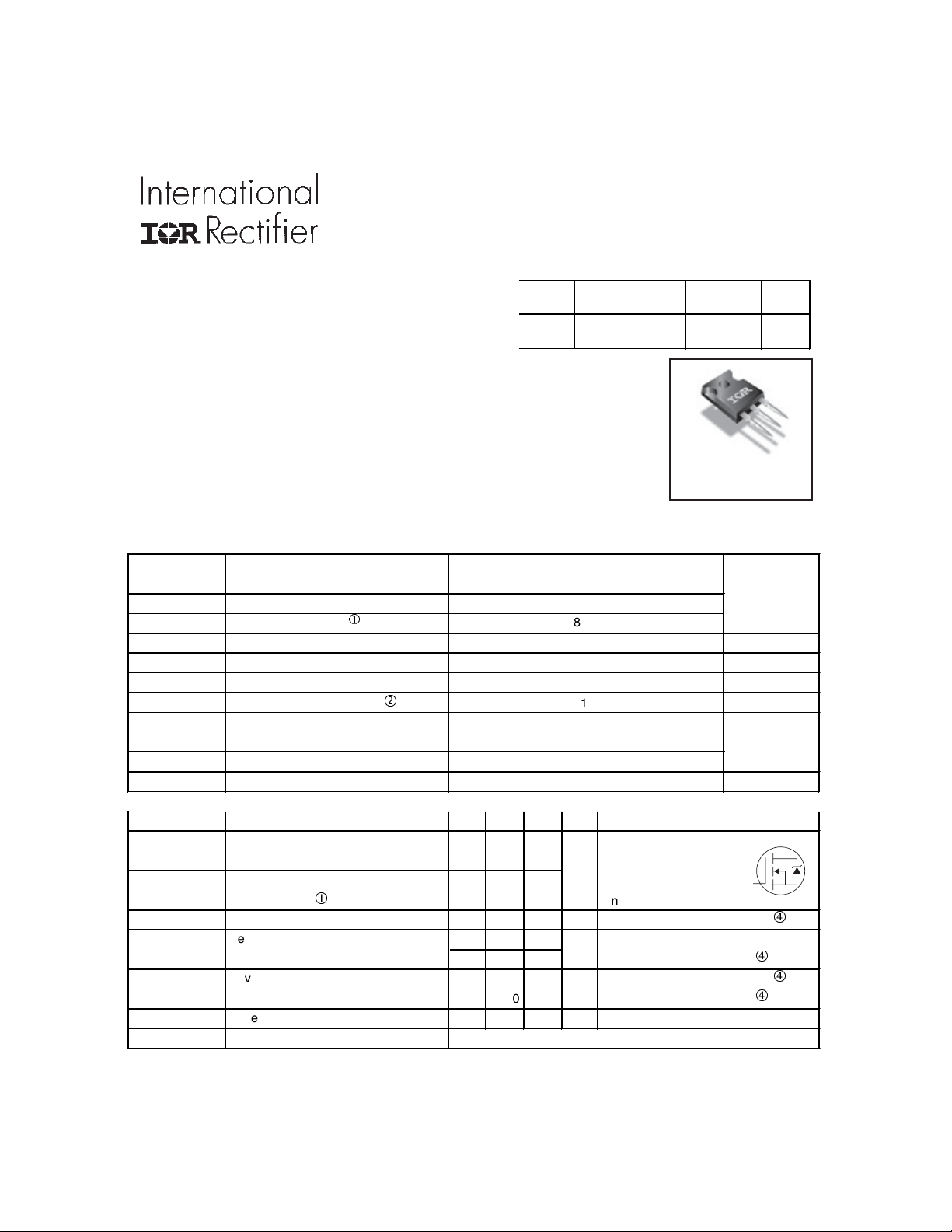
TO-247AC
.
Conditions
G
= 25°C, IS = 21A, VGS = 0V
J
= 25°C, IF = 21A
J
= 125°C, di/dt = 100A/µs
J
= 25°C, IS = 21A, VGS = 0V
J
= 125°C, di/dt = 100A/µs
J
= 25°C
J
I
D
f
f
7/16/04
D
S
Page 2
IRFP21N60LPbF
/
Single Pulse Aval
gy
d
Aval
c
R
gy
c
Document Number: 91206
www.vishay.com
2
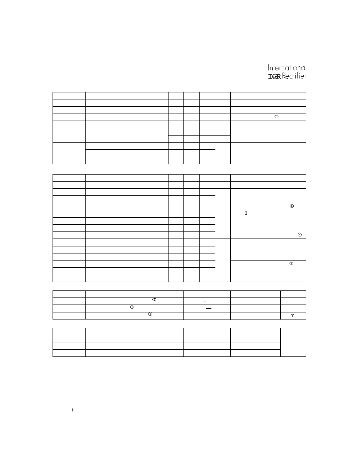
Static @ TJ = 25°C (unless otherwise specified)
Symbol Parameter Min. Typ. Max. Units
V
(BR)DSS
∆
V
R
DS(on)
V
GS(th)
I
DSS
I
GSS
R
G
(BR)DSS
Drain-to-Source Breakdown Voltage 600 ––– ––– V
∆
T
Breakdown Voltage Temp. Coefficient ––– 0.42 ––– V/°C
J
Static Drain-to-Source On-Resistance ––– 270 320
Gate Threshold Voltage 3.0 ––– 5.0 V
Drain-to-Source Leakage Current ––– ––– 50 µA
––– ––– 2.0 mA
Gate-to-Source Forward Leakage ––– ––– 100 nA
Gate-to-Source Reverse Leakage ––– ––– -100
Internal Gate Resistance ––– 0.63 –––
VGS = 0V, ID = 250µA
Reference to 25°C, I
V
mΩ
GS
V
DS
V
DS
V
DS
V
GS
V
GS
Ω
f = 1MHz, open drain
Dynamic @ TJ = 25°C (unless otherwise specified)
Symbol Parameter Min. Typ. Max. Units
gfs Forward Transconductance 11 ––– ––– S
Q
Q
Q
t
t
t
t
C
C
C
C
C
g
gs
gd
d(on)
r
d(off)
f
iss
oss
rss
oss
oss
eff.
eff. (ER)
Total Gate Charge ––– ––– 150
Gate-to-Source Charge ––– ––– 46 nC
Gate-to-Drain ("Miller") Charge ––– ––– 64
Turn-On Delay Time ––– 20 –––
Rise Time ––– 58 ––– ns
Turn-Off Delay Time ––– 33 –––
Fall Time ––– 10 –––
Input Capacitance ––– 4000 –––
Output Capacitance ––– 340 –––
Reverse Transfer Capacitance ––– 29 ––– pF
Effective Output Capacitance ––– 170 –––
Effective Output Capacitance ––– 130 –––
(Energy Related)
VDS = 50V, ID = 13A
I
= 21A
D
V
DS
V
GS
VDD = 300V
ID = 21A
R
G
V
GS
VGS = 0V
V
DS
ƒ = 1.0MHz, See Fig. 5
V
GS
Avalanche Characteristics
Symbol
E
AS
I
AR
E
AR
anche Current
epetitive Avalanche Ener
Parameter Typ. Units
anche Ener
––– mJ
––– A
––– mJ
Thermal Resistance
Symbol Parameter Typ. Units
R
JC
θ
R
CS
θ
R
JA
θ
Notes:
Repetitive rating; pulse width limited by
max. junction temperature. (See Fig. 11)
Starting T
I
= 21A, dv/dt = 11V/ns. (See Figure 12a)
AS
I
≤ 21A, di/dt ≤ 530A/µs, V
SD
TJ ≤ 150°C.
Junction-to-Case –––
Case-to-Sink, Flat, Greased Surface 0.24 °C/W
Junction-to-Ambient ––– 40
Pulse width ≤ 300µs; duty cycle ≤ 2%.
C
eff. is a fixed capacitance that gives the same charging time
oss
as C
= 25°C, L = 1.9mH, RG = 25Ω,
J
≤ V
DD
(BR)DSS
,
while VDS is rising from 0 to 80% V
oss
C
eff.(ER) is a fixed capacitance that stores the same energy
oss
as C
while VDS is rising from 0 to 80% V
oss
Conditions
= 1mA
D
= 10V, ID = 13A
f
= VGS, ID = 250µA
= 600V, VGS = 0V
= 480V, VGS = 0V, TJ = 125°C
= 30V
= -30V
Conditions
= 480V
= 10V, See Fig. 7 & 15
= 1.3Ω
= 10V, See Fig. 11a & 11b
= 25V
= 0V,VDS = 0V to 480V
Max.
420
21
33
Max.
0.38
–––
.
DSS
.
DSS
f
f
g
Page 3
IRFP21N60LPbF
Document Number: 91206
www.vishay.com
3
1000
TOP 15V
100
)
A
(
t
n
e
r
10
r
u
C
e
c
r
u
o
S
o
t
n
i
a
r
D
,
D
I
BOTTOM 5.5V
1
0.1
0.01
VGS
12V
10V
8.0V
7.0V
6.5V
6.0V
5.5V
20µs PULSE WIDTH
Tj = 25°C
0.001
0.1 1 10 100 1000
VDS, Drain-to-Source Voltage (V)
1000
)
Α
100
(
t
n
e
r
r
u
C
10
e
c
r
u
o
S
-
1
o
t
n
i
a
r
D
,
0.1
D
I
TJ = 25°C
TJ = 150°C
V
= 50V
DS
20µs PULSE WIDTH
0.01
4 6 8 10 12 14 16
VGS, Gate-to-Source Voltage (V)
100
TOP 15V
)
A
(
t
10
n
e
r
r
u
C
e
c
r
u
o
S
o
t
n
i
a
r
D
,
D
I
BOTTOM 5.5V
1
0.1
VGS
12V
10V
8.0V
7.0V
6.5V
6.0V
20µs PULSE WIDTH
Tj = 150°C
0.01
0.1 1 10 100
VDS, Drain-to-Source Voltage (V)
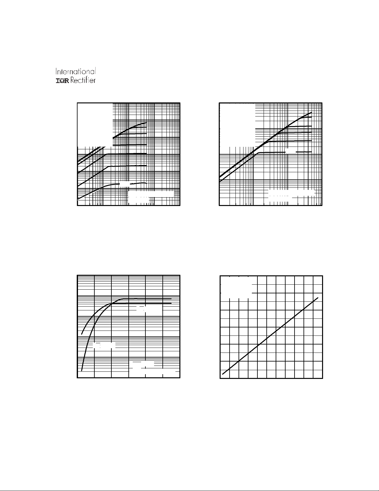
Fig 2. Typical Output CharacteristicsFig 1. Typical Output Characteristics
3.0
e
c
n
a
t
s
i
s
e
R
n
O
e
c
r
u
o
S
o
t
n
i
a
r
D
,
)
n
o
(
S
D
R
ID = 21A
V
= 10V
GS
2.5
2.0
)
d
e
z
i
1.5
l
a
m
r
o
N
(
1.0
0.5
0.0
-60 -40 -20 0 20 40 60 80 100 120 140 160
TJ , Junction Temperature (°C)
5.5V
Fig 3. Typical Transfer Characteristics
Fig 4. Normalized On-Resistance
vs. Temperature
Page 4
IRFP21N60LPbF
Document Number: 91206
www.vishay.com
4
100000
10000
)
F
p
(
e
c
n
a
t
i
1000
c
a
p
a
C
,
C
100
10
V
= 0V, f = 1 MHZ
GS
C
= C
= C
= C
+ Cgd, C
gs
gd
+ C
ds
C
iss
C
oss
C
rss
iss
C
rss
C
oss
1 10 100 1000
VDS, Drain-to-Source Voltage (V)
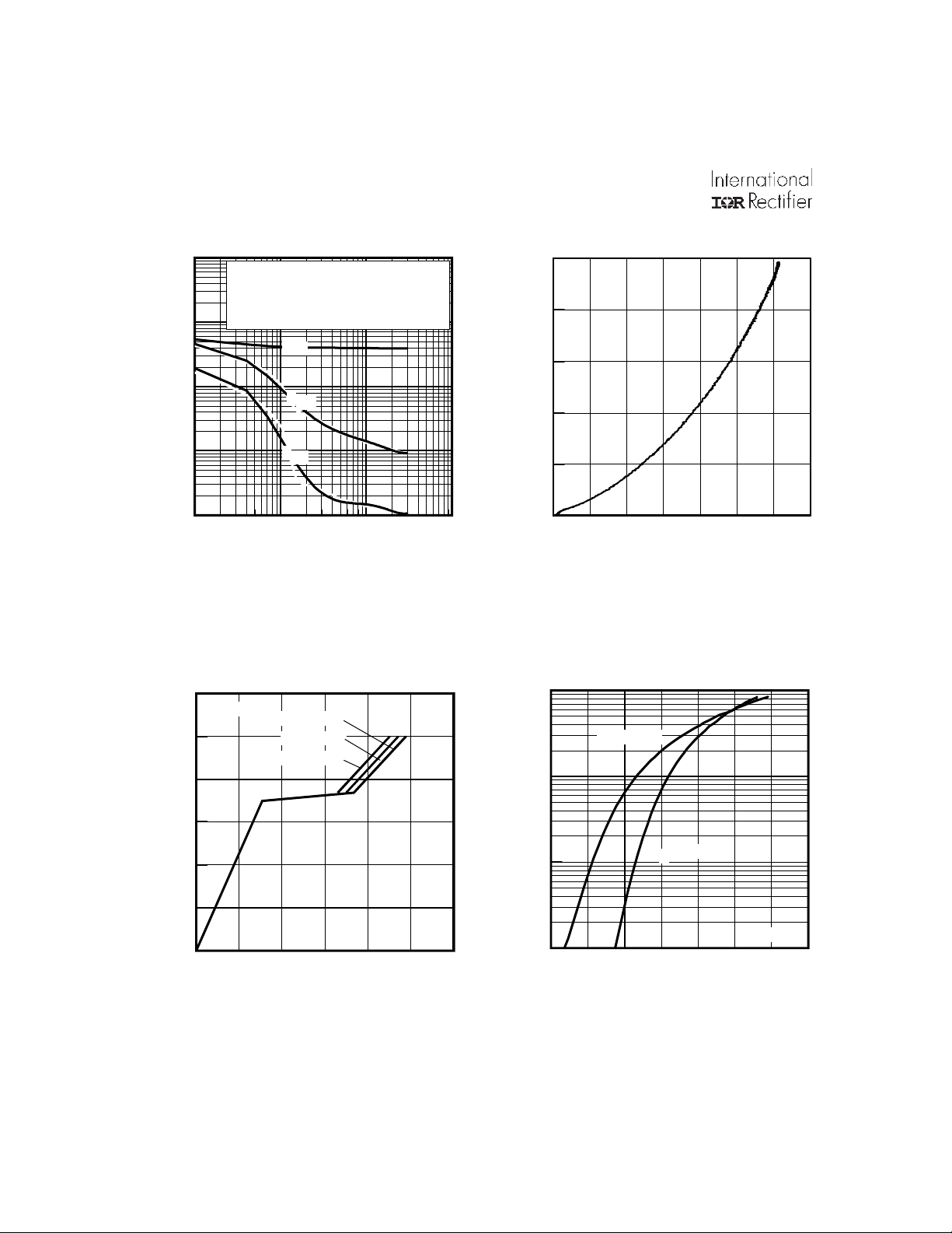
Fig 5. Typical Capacitance vs.
Drain-to-Source Voltage
12.0
ID= 21A
)
10.0
V
(
e
g
a
t
l
8.0
o
V
e
c
r
u
6.0
o
S
o
t
e
t
4.0
a
G
,
S
G
2.0
V
0.0
0 20 40 60 80 100 120
VDS= 480V
VDS= 300V
VDS= 120V
Q
Total Gate Charge (nC)
G
25
SHORTED
ds
gd
20
)
15
J
µ
(
y
g
r
e
n
10
E
5
0
0 100 200 300 400 500 600 700
V
Drain-to-Source Voltage (V)
DS,
Fig 6. Typ. Output Capacitance
100.00
)
A
(
t
n
e
r
10.00
r
u
C
n
i
a
r
D
e
s
r
e
v
1.00
e
R
,
D
S
I
0.10
Stored Energy vs. V
TJ = 150°C
TJ = 25°C
0.2 0.4 0.6 0.8 1.0 1.2 1.4 1.6
VSD, Source-to-Drain Voltage (V)
DS
V
GS
= 0V
Fig 7. Typical Gate Charge vs.
Gate-to-Source Voltage
Fig 8. Typical Source-Drain Diode
Forward Voltage
Page 5
IRFP21N60LPbF
Document Number: 91206
www.vishay.com
5
1000
OPERATION IN THIS AREA
)
A
(
t
n
e
r
r
u
C
e
c
r
u
o
S
o
t
n
i
a
r
D
,
I
100
D
10
1
Tc = 25°C
Tj = 150°C
LIMITED BY RDS(on)
100µsec
1msec
10msec
Single Pulse
0.1
1 10 100 1000 10000
VDS, Drain-to-Source Voltage (V)
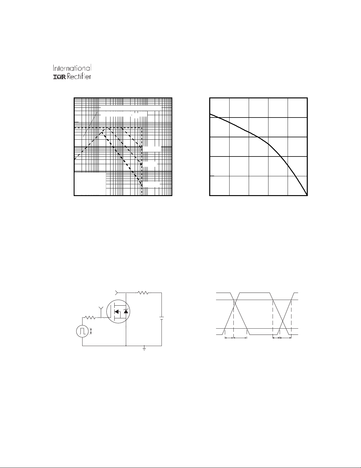
Fig 9. Maximum Safe Operating Area
25
20
)
A
(
t
n
15
e
r
r
u
C
n
i
a
r
10
D
,
D
I
5
0
25 50 75 100 125 150
TC , Case Temperature (°C)
Fig 10. Maximum Drain Current vs.
Case Temperature
R
V
DS
V
GS
R
G
D
D.U.T.
10V
Pulse Width ≤ 1 µs
Duty Factor ≤ 0.1 %
Fig 11a. Switching Time Test Circuit
V
DS
90%
+
V
DD
-
10%
V
GS
t
d(on)tr
t
d(off)tf
Fig 11b. Switching Time Waveforms
Page 6
IRFP21N60LPbF
Document Number: 91206
www.vishay.com
6
1
)
C
J
h
t
Z
(
e
s
n
0.01
o
p
s
e
R
l
a
m
r
e
0.001
h
T
0.0001
0.1
D = 0.50
0.20
0.10
0.05
0.02
0.01
SINGLE PULSE
( THERMAL RESPONSE )
1E-006 1E-005 0.0001 0.001 0.01 0.1 1
Not es:
1. Duty factor D = t / t
2. Peak T = P x Z + T
J DM thJC C
1 2
P
DM
t
1
t1 , Rectangular Pulse Duration (sec)
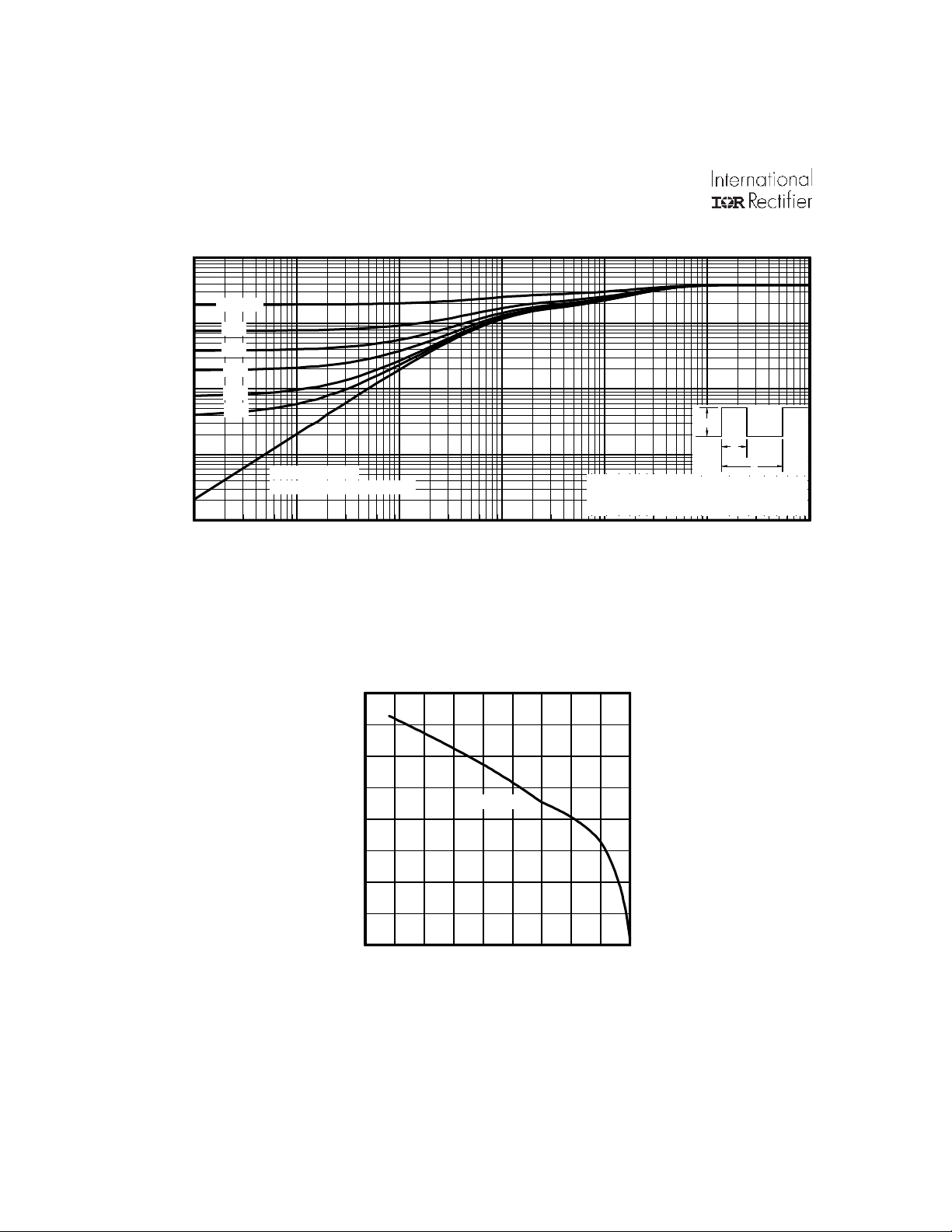
Fig 12. Maximum Effective Transient Thermal Impedance, Junction-to-Case
5.0
)
V
(
e
g
4.0
a
t
l
o
V
d
l
o
h
s
3.0
e
r
h
t
e
t
a
G
)
h
2.0
t
(
S
G
V
ID = 250µA
t
2
1.0
-75 -50 -25 0 25 50 75 100 125 150
TJ , Temperature ( °C )
Fig 13. Threshold Voltage vs. Temperature
Page 7
IRFP21N60LPbF
A
Document Number: 91206
www.vishay.com
7
800
)
J
m
(
700
y
g
r
e
600
n
E
e
h
500
c
n
a
l
a
400
v
A
e
s
l
300
u
P
e
l
g
200
n
i
S
,
100
S
A
E
0
25 50 75 100 125 150
TOP 9.4A
BOTTOM21A
Starting TJ , Junction Temperature (°C)
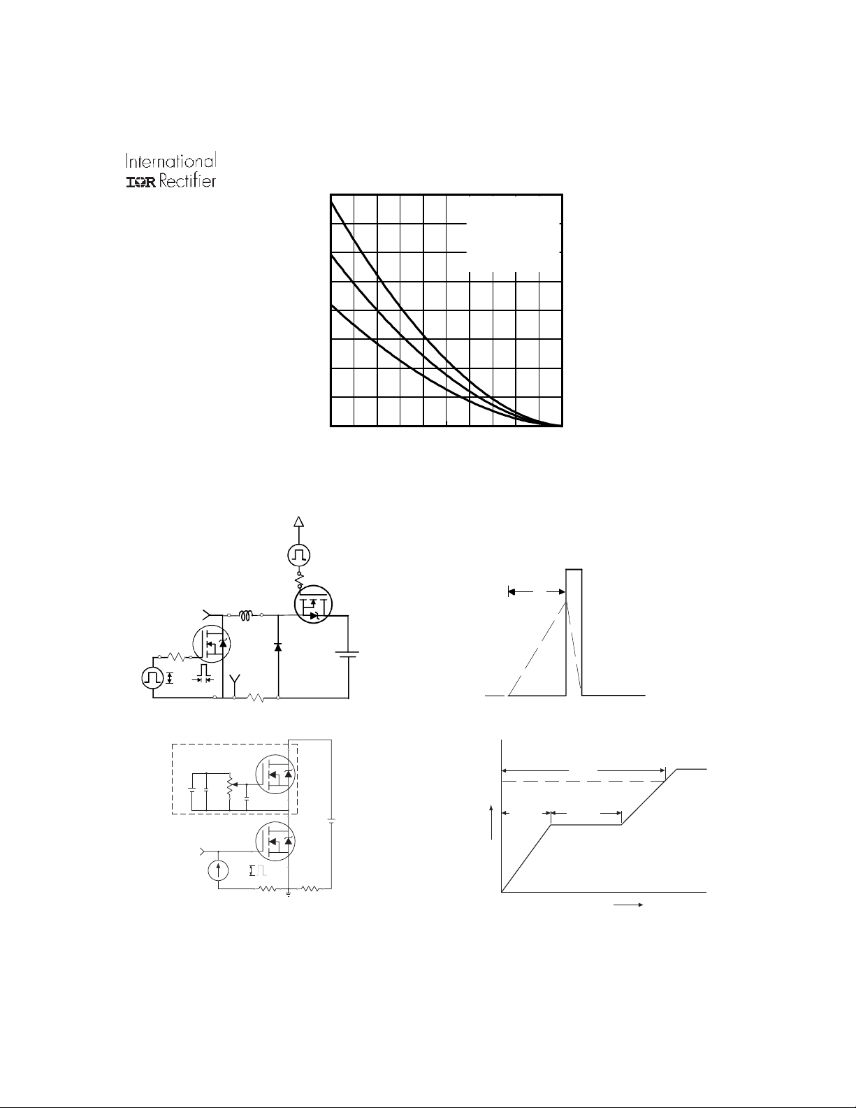
Fig 14a. Maximum Avalanche Energy
vs. Drain Current
15V
V
DS
L
DRIVER
I
D
13A
V
(BR)DSS
t
p
R
G
20V
D.U.T
I
AS
Ω
t
0.01
p
+
V
DD
-
Fig 14b. Unclamped Inductive Test Circuit
Current Regulator
Same Type as D.U.T.
50KΩ
.2µF
12V
V
GS
.3µF
D.U.T.
3mA
I
G
Current Sampling Resistors
+
V
DS
-
I
D
Fig 15a. Gate Charge Test Circuit
I
AS
Fig 14c. Unclamped Inductive Waveforms
Q
G
VGS V
Q
GS
V
G
Q
GD
Charge
Fig 15b. Basic Gate Charge Waveform
Page 8
IRFP21N60LPbF
Document Number: 91206
www.vishay.com
8
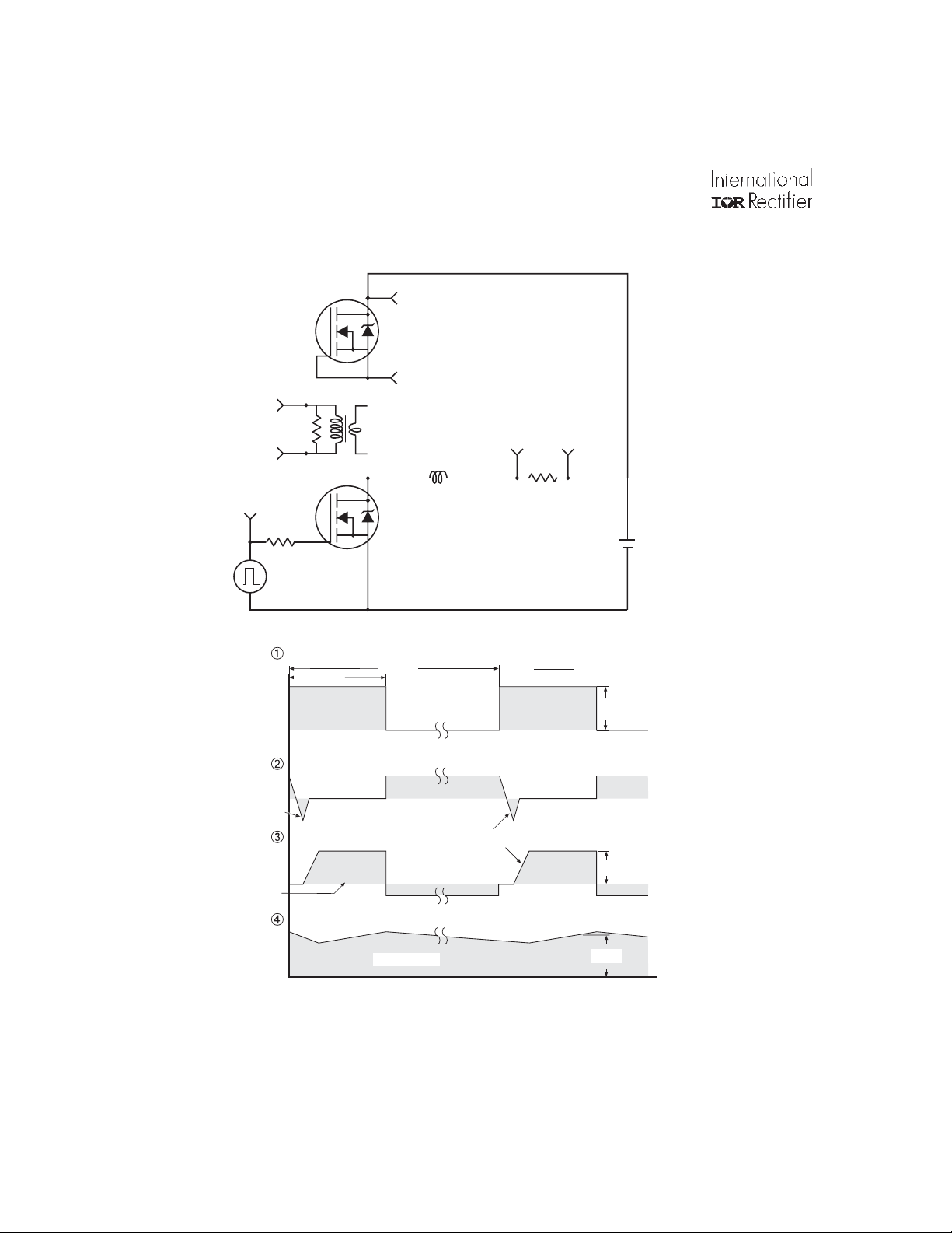
Peak Diode Recovery dv/dt Test Circuit
+
D.U.T
-
R
G
Driver Gate Drive
P.W.
+
Circuit Layout Considerations
• Low Stray Inductance
• Ground Plane
• Low Leakage Inductance
Current Transformer
-
-
• dv/dt controlled by R
• Driver same type as D.U.T.
G
• ISD controlled by Duty Factor "D"
• D.U.T. - Device Under Test
Period
D =
P. W .
Period
+
+
V
DD
-
VGS=10V
*
Reverse
Recovery
Current
Re-Applied
Voltage
D.U.T. ISDWaveform
Body Diode Forward
Current
D.U.T. VDSWaveform
Body Diode Forward Drop
Inductor Curent
Ripple ≤ 5%
* V
= 5V for Logic Level Devices
GS
di/dt
Diode Recovery
dv/dt
V
DD
I
SD
Fig 16. For N-Channel HEXFET® Power MOSFETs
Page 9
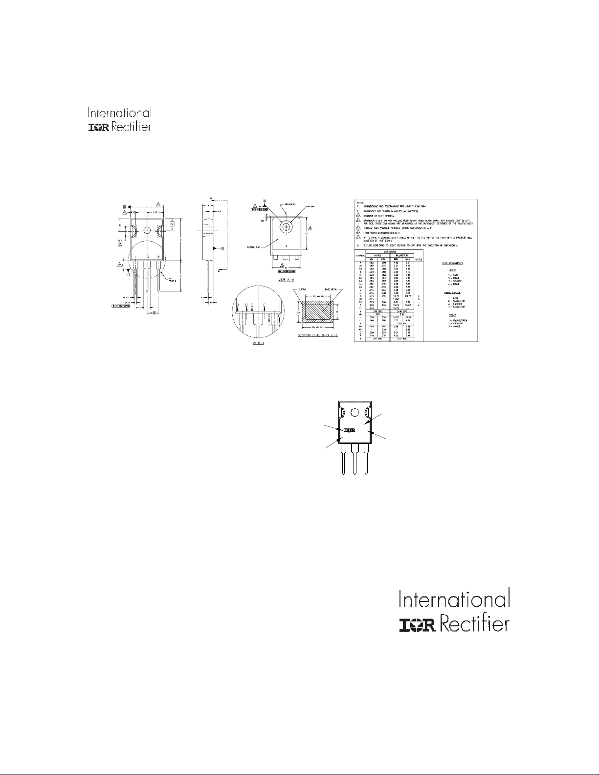
TO-247AC Package Outline
Document Number: 91206
www.vishay.com
9
Dimensions are shown in millimeters (inches)
TO-247AC Part Marking Information
IRFP21N60LPbF
EXAMPLE:
THIS IS AN IRFPE 30
WITH ASSEMBLY
LOT CODE 5657
ASS EMB LED ON WW 35, 2000
IN THE AS SEMBLY LINE "H"
Note: "P" in assembly line
positio n indicates "L ead-Free"
INTER NATIONAL
RECTIF IER
LOGO
ASSEMBLY
LOT CODE
IRFPE30
56 57
035H
PART NUMBER
DAT E CODE
YEAR 0 = 2000
WE EK 35
LINE H
TO-247AC package is not recommended for Surface Mount Application.
Data and specifications subject to change without notice.
This product has been designed and qualified for the Industrial market.
Qualification Standards can be found on IR’s Web site.
IR WORLD HEADQUARTERS: 233 Kansas St., El Segundo, California 90245, USA Tel: (310) 252-7105
TAC Fax: (310) 252-7903
07/04
Page 10

Legal Disclaimer Notice
Vishay
Notice
The products described herein were acquired by Vishay Intertechnology, Inc., as part of its acquisition of
International Rectifier’s Power Control Systems (PCS) business, which closed in April 2007. Specifications of the
products displayed herein are pending review by Vishay and are subject to the terms and conditions shown below.
Specifications of the products displayed herein are subject to change without notice. Vishay Intertechnology, Inc., or
anyone on its behalf, assumes no responsibility or liability for any errors or inaccuracies.
Information contained herein is intended to provide a product description only. No license, express or implied, by
estoppel or otherwise, to any intellectual property rights is granted by this document. Except as provided in Vishay's
terms and conditions of sale for such products, Vishay assumes no liability whatsoever, and disclaims any express
or implied warranty, relating to sale and/or use of Vishay products including liability or warranties relating to fitness
for a particular purpose, merchantability, or infringement of any patent, copyright, or other intellectual property right.
The products shown herein are not designed for use in medical, life-saving, or life-sustaining applications.
Customers using or selling these products for use in such applications do so at their own risk and agree to fully
indemnify Vishay for any damages resulting from such improper use or sale.
International Rectifier
are registered trademarks of International Rectifier Corporation in the U.S. and other countries. All other product
names noted herein may be trademarks of their respective owners.
®
, IR®, the IR logo, HEXFET®, HEXSense®, HEXDIP®, DOL®, INTERO®, and POWIRTRAIN
®
Document Number: 99901 www.vishay.com
Revision: 12-Mar-07 1
 Loading...