

Page 1
Provisional Data Sheet No. PD-9.1547
Next Data SheetIndex
Previous Datasheet
To Order
®
HEXFET
100 V olt, 0.060
POWER MOSFET
ΩΩ
Ω HEXFET
ΩΩ
HEXFET technology is the key to International Rectifier’s
advanced line of power MOSFET transistors. The efficient geometry achieves very low on-state resistance combined with high transconductance.
HEXFET transistors also feature all of the well-establish
advantages of MOSFETs, such as voltage control, very
fast switching, ease of paralleling and electrical parameter temperature stability . They are well-suited for applications such as switching power supplies, motor controls,
inverters, choppers, audio amplifiers, and high energy
pulse circuits.
The Surface Mount Device (SMD-1) package represents
another step in the continual evolution of surface mount
technology . The SMD-1 will give designers the extra flexibility they need to increase circuit board density . International Rectifier has engineered the SMD-1 package to
meet the specific needs of the power market by increasing the size of the termination pads, thereby enhancing
thermal and electrical performance.
IRFN150
N-CHANNEL
Product Summary
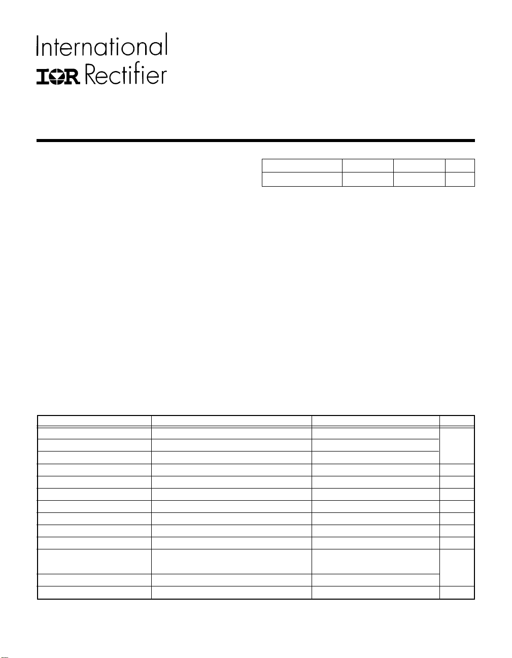
Part Number BVDSS RDS(on) I D
IRFN150 100V 0.060Ω 34A
Features:
■ Avalanche Energy Rating
■ Dynamic dv/dt Rating
■ Simple Drive Requirements
■ Ease of Paralleling
■ Hermetically Sealed
■ Surface Mount
■ Light-weight
Absolute Maximum Ratings
ID @ VGS = 10V , TC = 25°C Continuous Drain Current 34
ID @ VGS = 10V, TC = 100°C Continuous Drain Current 21
I
DM
PD @ TC = 25°C Max. Power Dissipation 150 W
V
GS
E
AS
I
AR
E
AR
dv/dt Peak Diode Recovery dv/dt ➂ 5.5
T
J
T
STG
Parameter IRFN150 Units
A
Pulsed Drain Current ➀ 136
Linear Derating Factor 1.2 W/K ➄
Gate-to-Source Voltage ±20 V
Single Pulse Avalanche Energy ➁ 150 mJ
Avalanche Current ➀ 34 A
Repetitive Avalanche Energy ➀ 15 mJ
V/ns
Operating Junction -55 to 150
Storage Temperature Range
Package Mounting Surface Temperature 300
Weight 2.6 (typical) g
(for 5 seconds)
o
C
Page 2

IRFN150 Device
Next Data SheetIndex
Previous Datasheet
To Order
Electrical Characteristics @ Tj = 25°C (Unless Otherwise Specified)
Parameter Min. Typ. Max. Units Test Conditions
BV
DSS
∆BV
R
DS(on)
V
GS(th)
g
fs
I
DSS
I
GSS
I
GSS
Q
g
Q
gs
Q
gd
t
d(on)
t
r
t
d(off)
t
f
L
D
L
S
C
iss
C
oss
C
rss
DSS
Drain-to-Source Breakdown Voltage 100 — — V VGS = 0V, ID = 1.0 mA
/∆TJTemperature Coefficient of Breakdown — 0.13 — V/°C Reference to 25°C, ID = 1.0 mA
Voltage
Static Drain-to-Source — — 0.060 VGS = 10V, ID = 21A
On-State Resistance — — 0.070 Ω VGS = 10V, ID = 34A
Gate Threshold Voltage 2.0 — 4.0 V VDS = VGS, ID = 250µA
Forward Transconductance 9 — — S ( )VDS > 15V, IDS = 21A ➃
Zero Gate Voltage Drain Current — — 25 VDS = 0.8 x Max Rating,VGS = 0V
— — 250 VDS = 0.8 x Max Rating
Gate-to-Source Leakage Forward — — 100 VGS = 20V
Gate-to-Source Leakage Reverse — — -100 VGS = -20V
Total Gate Charge 50 — 125 VGS =10V, ID = 34A
Gate-to-Source Charge 8 — 22 VDS = Max. Rating x 0.5
Gate-to-Drain (“Miller”) Charge 15 — 65 see figures 6 and 13
Turn-On Delay Time — — 35 VDD = 50V, ID = 34A,
Rise Tim e — — 190 RG = 2.35Ω, VGS = 10V
Turn-Off Delay Time — — 1 70
Fall Time — — 130 see figure 10
Internal Drain Inductance — 2.0 —
Internal Source Inductance — 4.1 —
Input Capacitance — 3700 — VGS = 0V, VDS = 25V
Output Capacitance — 1100 — f = 1.0 MHz
Reverse Transfer Capacitance — 200 — see figure 5
Ω
µA
nA
nC
ns
Measured from the
drain lead, 6mm (0.25
in.) from package to
center of die.
nH
Measured from the
source lead, 6mm
(0.25 in.) from package
to source bonding pad.
pF
VGS = 0V, TJ = 125°C
Modified MOSFET
symbol showing the
internal inductances.
➃
Source-Drain Diode Ratings and Characteristics
Parameter Min. Typ. Max. Units Test Conditions
I
Continuous Source Current (Body Diode) — — 34 Modified MOSFET symbol showing the
S
I
Pulse Source Current (Body Diode) ➀ — — 136 integral reverse p-n junction rectifier.
SM
V
Diode Forward Voltage — — 1.8 V Tj = 25°C, IS = 34A, VGS = 0V ➃
SD
t
Reverse Recovery Time — — 500 ns Tj = 25°C, IF = 34A, di/dt ≤ 100A/µs
rr
Q
Reverse Recovery Charge — — 2.9 µCV
RR
t
Forward Turn-On Time
on
Intrinsic turn-on time is negligible. T urn-on speed is substantially controlled by LS + LD.
Thermal Resistance
Parameter Min. Typ. Max. Units Test Conditions
R
thJC
R
thJ-PCB
Junction-to-Case — — 0.83
Junction-to-PC Board — TBD — K/W Soldered to a copper clad PC board
A
≤ 50V ➃
DD
Page 3

IRFN150 Device
To Order
Next Data SheetIndex
Previous Datasheet
Fig. 1 — Typical Output Characteristics
Fig. 3 — Typical Transfer Characteristics
T
C
= 25°C
Fig. 2 — Typical Output Characteristics
TC = 150°C
ID = 34A
Fig. 4 — Normalized On-Resistance Vs.Temperature
ID = 34A
Fig. 5 — Typical Capacitance Vs. Drain-to-Source
Voltage
Fig. 6 — Typical Gate Charge Vs. Gate-to-Source
Voltage
Page 4
IRFN150 Device
To Order
Next Data SheetIndex
Previous Datasheet
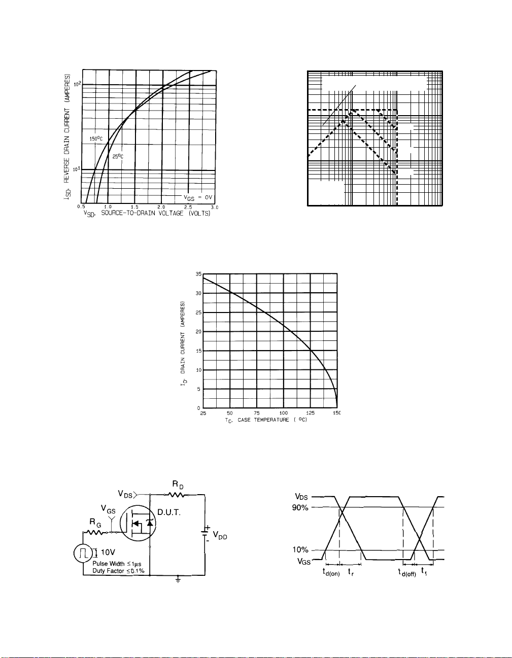
Fig. 7 — Typical Source-to-Drain Diode Forward
Voltage
1000
I , Drain Current (A)I , Drain Current (A)
OPERATION IN THIS AREA LIMITED
100
10
D
= 25 C
C
T T= 150 C
J
Single Pulse
1
1 10 100 1000
V , Drain-to-Source Voltage (V)
DS
BY R
DS(on)
100us
1ms
10ms
°
°
Fig. 8 — Maximum Safe Operating Area
Fig. 10a — Switching Time Test Circuit
Fig. 9 — Maximum Drain Current Vs. Case Temperature
Fig. 10b — Switching Time Waveforms
Page 5
IRFN150 Device
To Order
Next Data SheetIndex
Previous Datasheet
1
0.50
0.20
thJC
0.1
0.10
0.05
0.02
0.01
0.01
Thermal Response (Z )
0.001
0.00001 0.0001 0.001 0.01 0.1 1
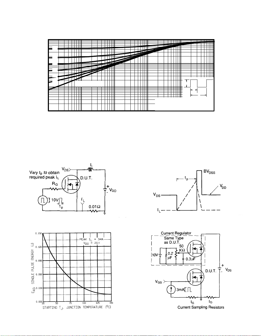
Fig. 11 — Maximum Effective Transient Thermal Impedance, Junction-to-Case Vs. Pulse Duration
SINGLE PULSE
(THERMAL RESPONSE)
Notes:
1. Duty factor D = t / t
2. Peak T = P x Z + T
t , Rectangular Pulse Duration (sec)
1
P
DM
1 2
J DM thJC C
t
1
t
2
Fig. 12a — Unclamped Inductive Test Circuit
Fig. 12c — Max. Avalanche Energy vs. Current Fig. 13a — Gate Charge Test Circuit
Fig. 12b — Unclamped Inductive Waveforms
Page 6
IRFN150 Device
To Order
Next Data SheetIndex
Previous Datasheet
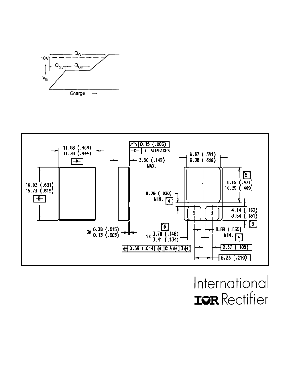
Fig. 13b — Basic Gate Charge Waveform
Case Outline and Dimensions — SMD-1
➀ Repetitive Rating; Pulse width limited by
maximum junction temperature.
(see figure 11)
➁ @ V
➂ I
➃ Pulse width ≤ 300 µs; Duty Cycle ≤ 2%
= 25V, Starting TJ = 25°C,
DD
EAS = [0.5 * L * (I
Peak IL = 34A, VGS = 10V, 25 ≤ RG ≤ 200Ω
≤ 34A, di/dt ≤ 200A/µs,
SD
VDD ≤ BV
, TJ ≤ 150°C
DSS
2
) * [BV
L
DSS
/(BV
DSS-VDD
➄ K/W = °C/W
W/K = W/°C
)]
All dimensions in millimeters (inches)
EUROPEAN HEADQUARTERS: Hurst Green, Oxted, Surrey RH8 9BB, UK Tel: ++ 44 1883 732020
IR FAR EAST: K&H Bldg., 2F, 3-30-4 Nishi-Ikeburo 3-Chome, Toshima-Ki, Tokyo Japan 171 Tel: 81 3 3983 0086
IR SOUTHEAST ASIA: 315 Outram Road, #10-02 Tan Boon Liat Building, Singapore 0316 Tel: 65 221 8371
WORLD HEADQUARTERS: 233 Kansas St., El Segundo, California 90245, Tel: (310) 322 3331
IR CANADA: 7321 Victoria Park Ave., Suite 201, Markham, Ontario L3R 2Z8, Tel: (905) 475 1897
http://www.irf.com/ Data and specifications subject to change without notice. 9/96
IR GERMANY: Saalburgstrasse 157, 61350 Bad Homburg Tel: ++ 49 6172 96590
IR ITALY: Via Liguria 49, 10071 Borgaro, Torino Tel: ++ 39 11 451 0111
 Loading...