

Page 1
PD -93988
IRFE9120
REPETITIVE A V ALANCHE AND dv/dt RA TED JANTX2N6845U
HEXFETTRANSISTORS
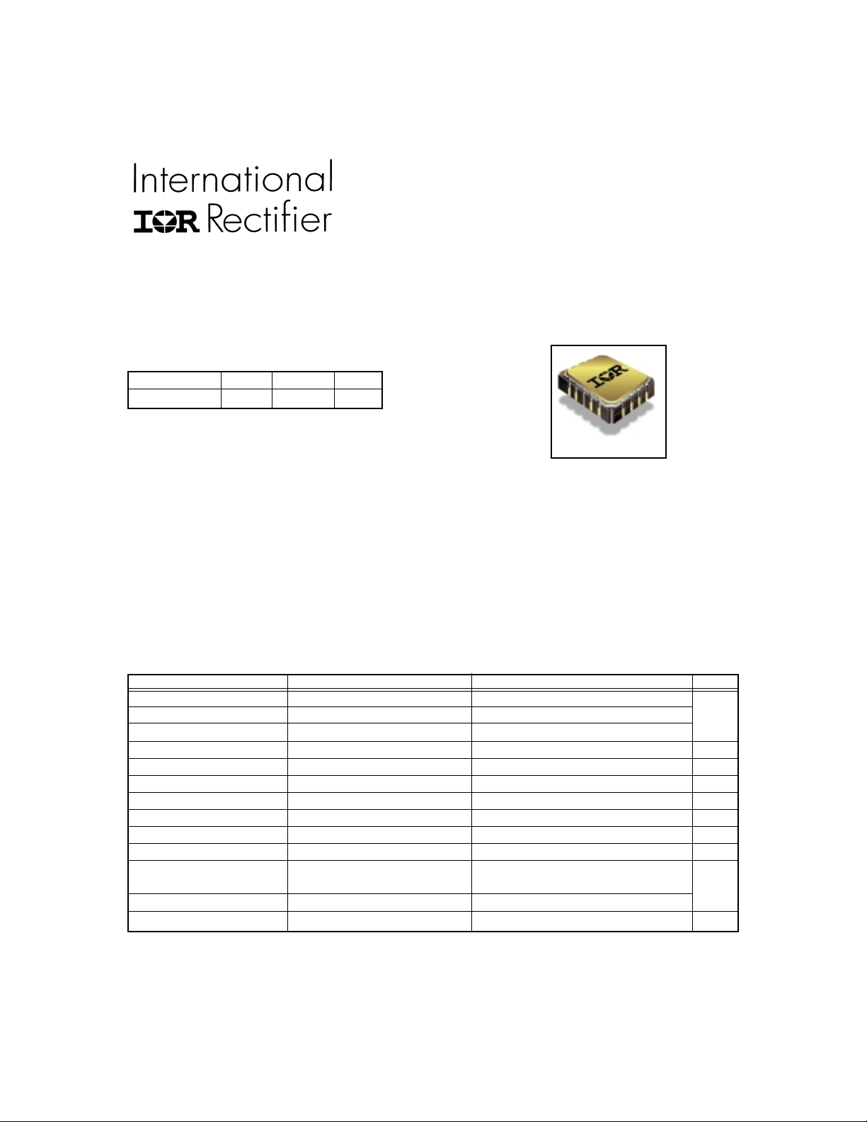
SURFACE MOUNT (LCC-18)
Product Summary
Part Number BVDSS RDS(on) ID
IRFE9120 -100V 0.60Ω −3.5A
[REF:MIL-PRF-19500/563]
JANTXV2N6845U
100V, P-CHANNEL
The leadless chip carrier (LCC) package represents the
logical next step in the continual evolution of surface
mount technology. Desinged to be a close replacement
for the TO-39 package, the LCC will give designers the
extra flexibility they need to increase circuit board density. International Rectifier has engineered the LCC package to meet the specific needs of the power market by
increasing the size of the bottom source pad, thereby
enhancing the thermal and electrical performance. The
lid of the package is grounded to the source to reduce
RF interference.
Features:
! Surface Mount
! Small Footprint
! Alternative to TO-39 Package
! Hermetically Sealed
! Dynamic dv/dt Rating
! Avalanche Energy Rating
! Simple Drive Requirements
! Light Weight
LCC-18
Absolute Maximum Ratings
Parameter Units
ID @ VGS = -10V, TC = 25°C Continuous Drain Current -3.5
ID @ VGS = -10V, TC = 100°C Continuous Drain Current -2.2
I
DM
PD @ TC = 25°C Max. Power Dissipation 1 4 W
V
GS
E
AS
I
AR
E
AR
dv/dt Peak Diode Recovery dv/dt ➂ -5.0
T
J
T
STG
Pulsed Drain Current ➀ -14
Linear Derating Factor 0.11 W/°C
Gate-to-Source Voltage ±2 0 V
Single Pulse Avalanche Energy ➁ 115 mJ
Avalanche Current ➀ -A
Repetitive Avalanche Energy ➀ -mJ
Operating Junction -55 to 150
Storage Temperature Range
Pckg. Mounting Surface Temp. 300 (for 5 S)
Weight 0.42(typical) g
A
V/ns
o
C
For footnotes refer to the last page
www.irf.com 1
10/25/00
Page 2
IRFE9120
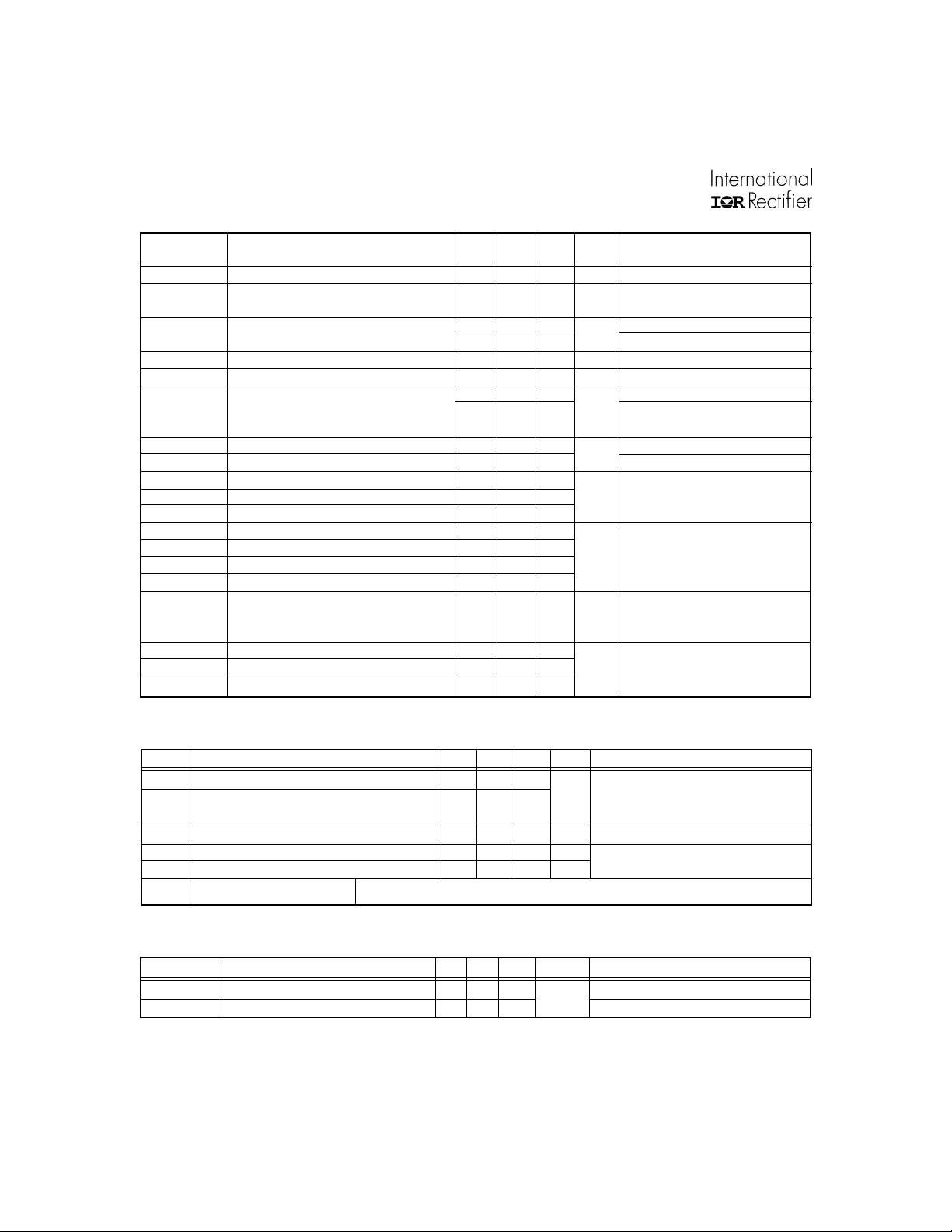
Electrical Characteristics @ Tj = 25°C (Unless Otherwise Specified)
Parameter Min Typ Max Units Test Conditions
BV
∆BV
R
V
g
I
I
I
Q
Q
Q
t
t
t
t
L
C
C
C
DSS
GSS
GSS
d(on)
r
d(off)
f
DSS
DSS
DS(on)
GS(th)
fs
g
gs
gd
S + LD
iss
oss
rss
Drain-to-Source Breakdown Voltage -100 — — V VGS = 0V, ID = -1.0mA
/∆TJTemperature Coefficient of Breakdown — -0. 10 — V/°C Reference to 25°C, ID =-1.0mA
Voltage
Static Drain-to-Source On-State — — 0.60 VGS =-10V, ID = -2.2A➃
Resistance — — 0.69 VGS =-10V, ID =-3.5A ➃
Gate Threshold Voltage -2.0 — -4.0 V VDS = VGS, ID =250µA
Forward Transconductance 1.25 — — S ( ) VDS >-15V, IDS =-2.2A➃
Zero Gate Voltage Drain Current — — - 25 VDS=-80V , VGS=0V
— — -250 VDS =-80V
Gate-to-Source Leakage Forward — — -100 VGS = -20V
Gate-to-Source Leakage Reverse — — 1 0 0 VGS = 20V
Total Gate Charge — — 16.3 VGS =-10V, ID= -3.5A
Gate-to-Source Charge — — 4.7 nC VDS =-50V
Gate-to-Drain (‘Miller’) Charge — — 9 .0
Turn-On Delay Time — — 6 0 VDD =- -50V, ID =-3.5A,
Rise Time — — 1 00 RG =7.5Ω
Turn-Off Delay Time — — 5 0
Fall Time — — 7 0
Total Inductance — 6 .1 —
Input Capacitance — 38 0 VGS = 0V, VDS = -25V
Output Capacitance — 170 — p F f = 1.0MHz
Reverse Transfer Capacitance — 45 —
Ω
Ω
µA
VGS = 0V, TJ = 125°C
nA
ns
nH
Measured from the center of
drain pad to center of source
pad
Source-Drain Diode Ratings and Characteristics
Parameter Min Typ Max Units Test Conditions
I
Continuous Source Current (Body Diode) — — -3.5
S
I
Pulse Source Current (Body Diode) ➀ — — -14
SM
V
Diode Forward Voltage — — -4.8 V Tj = 25°C, IS = -3.5A, VGS = 0V ➃
SD
t
Reverse Recovery Time — — 20 0 nS Tj = 25°C, IF =-3.5A, di/dt ≤ -100A/µs
rr
Q
Reverse Recovery Charge — — 3 .1 µc VDD ≤ -50V ➃
RR
t
Forward Turn-On Time Intrinsic turn-on time is negligible. Turn-on speed is substantially controlled by L
on
A
S
Thermal Resistance
Parameter Min Typ Max Units Test Conditions
R
thJC
R
thJ-PCB
For footnotes refer to the last page
2 www.irf.com
Junction to Case — — 9. 1
Junction to PC Board — — 26""" Soldered to a copper clad PC board
°C/W
+ LD.
Page 3
IRFE9120
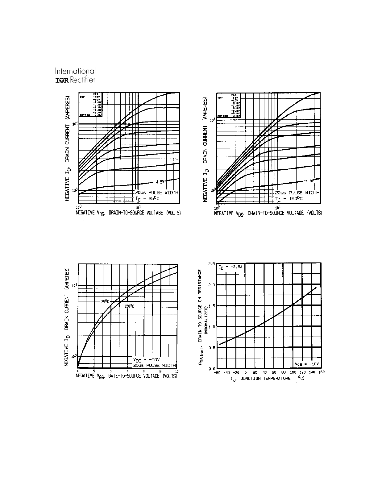
Fig 2. Typical Output CharacteristicsFig 1. Typical Output Characteristics
Fig 3. Typical Transfer Characteristics
Fig 4. Normalized On-Resistance
Vs. Temperature
www.irf.com 3
Page 4
IRFE9120
13 a& b
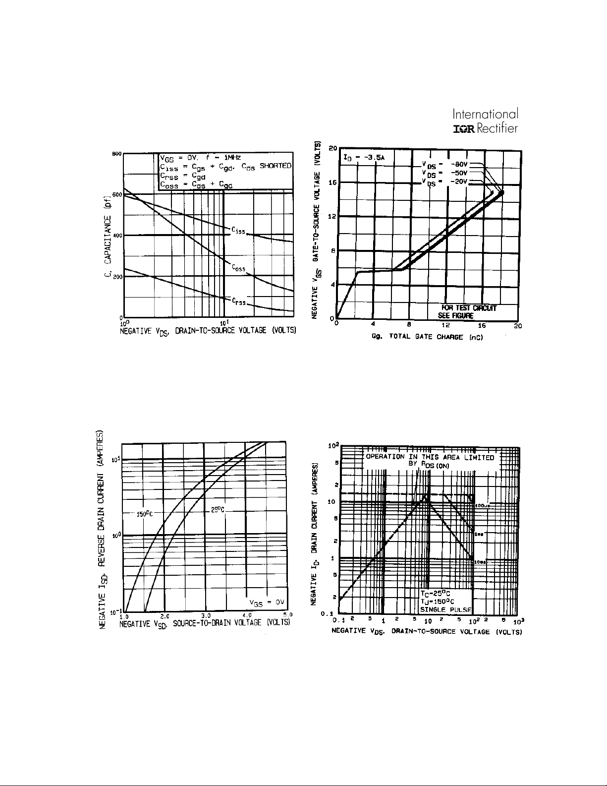
Fig 5. Typical Capacitance Vs.
Drain-to-Source Voltage
Fig 7. Typical Source-Drain Diode
Forward Voltage
Fig 6. Typical Gate Charge Vs.
Gate-to-Source Voltage
Fig 8. Maximum Safe Operating Area
4 www.irf.com
Page 5
IRFE9120
R
V
DS
V
GS
R
G
-10V
Pulse Width ≤ 1 µs
Duty Factor ≤ 0.1 %
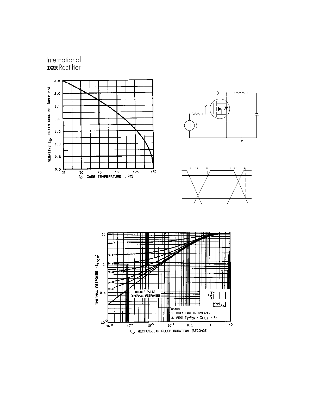
Fig 10a. Switching Time Test Circuit
D
D.U.T.
-
+
V
DD
Fig 9. Maximum Drain Current Vs.
Case Temperature
V
GS
10%
90%
V
DS
t
d(on)tr
t
d(off)tf
Fig 10b. Switching Time Waveforms
Fig 11. Maximum Effective Transient Thermal Impedance, Junction-to-Case
www.irf.com 5
Page 6
IRFE9120
(BR)
A
L
D.U.T
I
AS
0.01
p
DRIVER
Ω
15V
V
DD
R
V
G
-20V
10V
10V
DS
t
10V
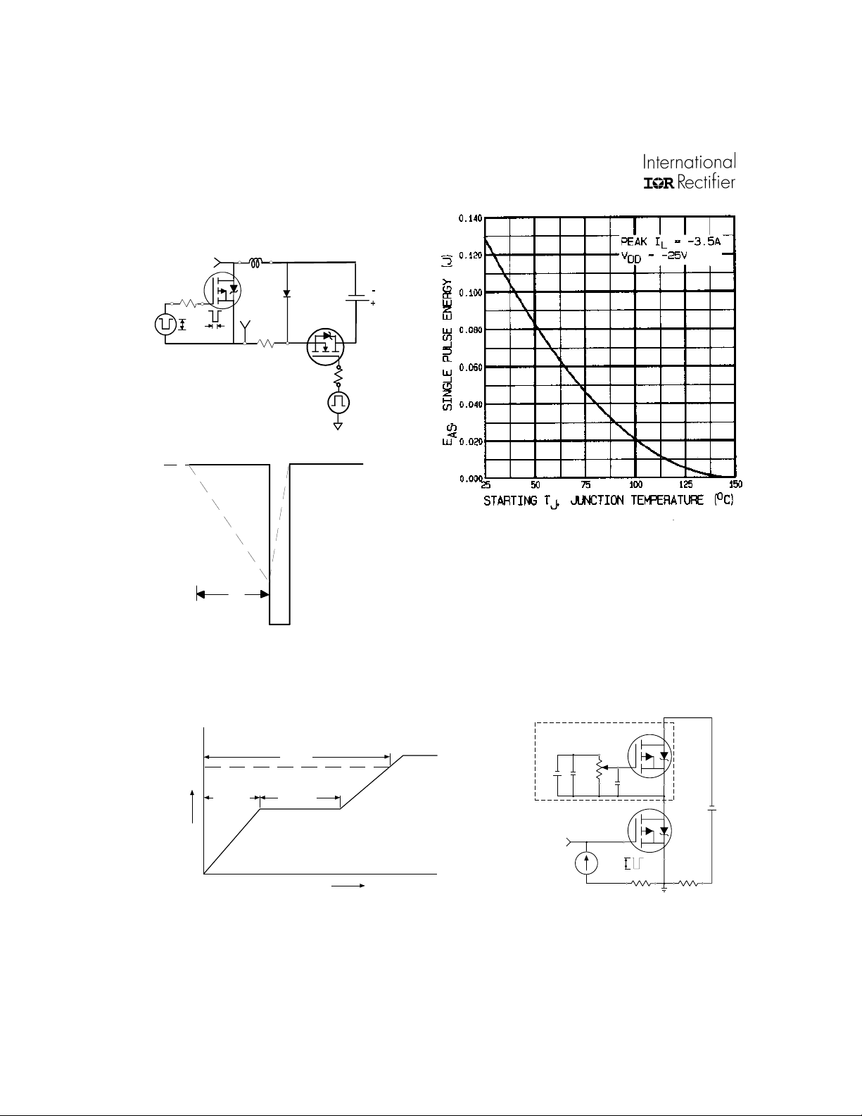
Fig 12a. Unclamped Inductive Test Circuit
I
AS
t
p
V
DSS
Fig 12c. Maximum Avalanche Energy
Vs. Drain Current
Fig 12b. Unclamped Inductive Waveforms
Current Regulator
Same Type as D.U.T.
Q
G
-10 V
Q
GS
V
G
Q
GD
Charge
Fig 13a. Basic Gate Charge Waveform
12V
V
GS
Fig 13b. Gate Charge Test Circuit
50KΩ
.2µF
.3µF
-3mA
Current Sampling Resistors
D.U.T.
I
G
I
D
6 www.irf.com
V
DS
+
Page 7
IRFE9120
Foot Notes:
➀ Repetitive Rating; Pulse width limited by
maximum junction temperature.
➁ V
=-25V, starting TJ = 25°C,
DD
Peak IL = -3.5A,
➃ Pulse width ≤ 300 µs; Duty Cycle ≤ 2%
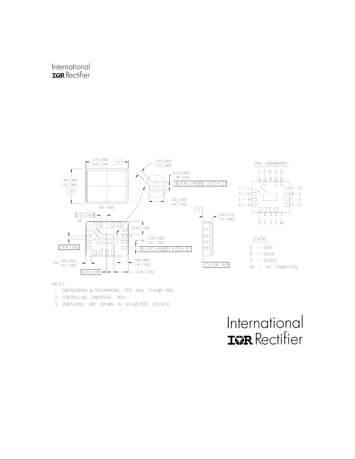
Case Outline and Dimensions — LCC-18
➂ I
≤ -3.5A, di/dt ≤ -110A/µs,
SD
VDD≤ -100V, TJ ≤ 150°C
Suggested RG =7.5 Ω
IR EUROPEAN REGIONAL CENTRE: 439/445 Godstone Rd, Whyteleafe, Surrey CR3 OBL, UK Tel: ++ 44 (0)20 8645 8000
IR SOUTHEAST ASIA: 1 Kim Seng Promenade, Great World City West Tower, 13-11, Singapore 237994 Tel: ++ 65 (0)838 4630
IR WORLD HEADQUARTERS: 233 Kansas St., El Segundo, California 90245, USA Tel: (310) 252-7105
IR CANADA: 15 Lincoln Court, Brampton, Ontario L6T3Z2, Tel: (905) 453 2200
IR GERMANY: Saalburgstrasse 157, 61350 Bad Homburg Tel: ++ 49 (0) 6172 96590
IR ITALY: Via Liguria 49, 10071 Borgaro, Torino Tel: ++ 39 011 451 0111
IR JAPAN: K&H Bldg., 2F, 30-4 Nishi-Ikebukuro 3-Chome, Toshima-Ku, Tokyo 171 Tel: 81 (0)3 3983 0086
IR TAIWAN:16 Fl. Suite D. 207, Sec. 2, Tun Haw South Road, Taipei, 10673 Tel: 886-(0)2 2377 9936
Data and specifications subject to change without notice. 10/00
www.irf.com 7
 Loading...