

Page 1

Applications
R
DS(on)
typ.
1.25m
Ω
PD - 96436
S trongIRFET
IRFB7434PbF
HEXFET® Power MOSFET
l Brushed Motor drive applications
l BLDC Motor drive applications
l Battery powered circuits
l Half-bridge and full-bridge topologies
l Synchronous rectifier applications
l Resonant mode power supplies
l OR-ing and redundant power switches
l DC/DC and AC/DC converters
l DC/AC Inverters
Benefits
l Improved Gate, Avalanche and Dynamic dV/dt
Ruggedness
l Fully Characterized Capacitance and Avalanche
SOA
l Enhanced body diode dV/dt and dI/dt Capability
l Lead-Free
V
D
DSS
40V
max. 1.6mΩ
G
I
D
(Silicon Limited)
S
I
D
(Package Limited)
D
D
G
317A
S
TO-220AB
IRFB7434PbF
GDS
Gate Drain Source
c
195A
Ordering Information
Base part number Package Type
IRFB7434PbF TO-220 Tube 50 IRFB7434PbF
)
5
Ω
m
(
e
c
n
4
a
t
s
i
s
e
R
n
3
O
e
c
r
u
o
S
2
o
t
n
i
a
r
D
1
,
)
n
o
(
S
D
0
R
2 4 6 8 10 12 14 16 18 20
V
Gate -to -Source Voltage (V)
GS,
ID = 100A
TJ = 125°C
TJ = 25°C
Standard Pack
Form Qua ntity
350
300
)
250
A
(
t
n
e
r
200
r
u
C
n
i
150
a
r
D
,
D
100
I
50
0
25 50 75 100 125 150 175
TC , Case Temperature (°C)
Complete Part Number
Limited By Package
Fig 1. Typical On-Resistance vs. Gate Voltage
Fig 2. Maximum Drain Current vs. Case Temperature
www.irf.com 1
04/20/12
Page 2

IRFB7434PbF
D
GS
J
STG
AR
AR
θ
θ
θ
JA
Max.
(BR)DSS
Δ
(BR)DSS
J
DS(on)
GS( th)
DSS
GSS
G
Conditions
D
DS
DS
DS
Absolute Maximum Ratings
Symbol Parameter Units
c
ID @ TC = 25°C Continuous Drain Current, VGS @ 10V (Silicon Limited)
I
@ TC = 100°C Continuous Drain Current, VGS @ 10V (Silicon Limited)
@ TC = 25°C Continuous Drain Current, VGS @ 10V (Wire Bond Limited)
I
D
I
DM
@TC = 25°C Maximum Power Dissipation W
P
D
Pulsed Drain Current
d
Linear Derating Factor W/°C
V
T
T
Gate-to -Source Voltage V
Operating Junction and
Storage Temperature Range
Soldering Temperature, for 10 seconds (1.6mm from case)
Mountin g torque, 6-32 or M3 screw
Avalanche Characteristics
E
AS (Thermally limited)
E
(tested) Single Pulse Avalanche Energy Tested Value
AS
I
E
Single Pulse Avalanche Energy
Avalanche Current
d
Repetitive Avalanche Energy
e
k
d
See Fig. 14, 15 , 22a, 22b
Thermal Resistance
Symbol Parameter Typ. Max. Units
R
JC
R
CS
R
Junction-to-Case
Case-to-Sink, Flat Greased Surface 0.50 –––
Junction-to-Ambient ––– 62
j
––– 0.51
317
c
224
195
1270
294
1.96
± 20
-55 to + 175
300
10lbfxin (1.1Nxm)
490
800
A
°C
mJ
A
mJ
°C/W
Static @ TJ = 25°C (unless otherwise specified)
Symbol Parameter Min. Typ. Max. Units
V
V
R
V
I
I
R
Notes:
Calculated continuous current based on maximum allowable junction
temperature. Bond wire current limit is 195A. Note that current
limitations arising from heating of the device leads may occur with
some lead mounting arrangements. (Refer to AN-1140)
Repetitive rating; pulse width limited by max. junction
temperature.
Limited by T
RG = 50Ω, I
I
≤ 100A, di/dt ≤ 1307A/μs, V
SD
Drain-to-Source Breakdown Voltage 40 ––– ––– V
Breakdown Voltage Temp. Coefficient ––– 0.032 ––– V/°C
/ΔT
Static Drain-to-Source On-Resistance ––– 1.25 1.6 mΩ
1.8 ––– mΩ
Gate Threshold Voltage 2.2 3.0 3.9 V
Drain-to-Source Leakage Current ––– ––– 1.0
––– ––– 150
Gate-to-Source Forward Leakage ––– ––– 100
Gate-to-Source Reverse Leakage ––– ––– -100
Internal Gate Resistance ––– 2.1 ––– Ω
Pulse width ≤ 400μs; duty cycle ≤ 2%.
C
eff. (TR) is a fixed capacitance that gives the same charging time
oss
, starting TJ = 25°C, L = 0.099mH
Jmax
= 100A, VGS =10V.
AS
DD
≤ V
(BR)DSS
as C
C
C
R
This value determined from sample failure population,
, TJ ≤ 175°C.
while V
oss
eff. (ER) is a fixed capacitance that gives the same energy as
oss
while V
oss
is measured at TJ approximately 90°C.
θ
starting TJ = 25°C, L=0.099mH, RG = 50Ω, I
is rising from 0 to 80% V
DS
is rising from 0 to 80% V
DS
VGS = 0V, ID = 250μA
Referen ce to 25°C, I
= 10V, ID = 100A
V
GS
= 6.0 V, ID = 50A
V
GS
= VGS, ID = 250μA
V
V
μA
nA
= 40V, VGS = 0V
V
= 40V, VGS = 0V, TJ = 125°C
V
= 20V
GS
= -20V
V
GS
.
DSS
.
DSS
= 100A, VGS =10V.
AS
= 5mA
g
g
d
2 www.irf.com
Page 3

Dynamic @ TJ = 25°C (unless otherwise specified)
g
sync
d(on)
r
iss
oss
rss
S
rr
J
RRM
DS
D
J
D
D
Symbol Parameter Min. Typ. Max. Units
gfs Forward Transconductance 211 ––– ––– S
Q
Q
gs
Q
gd
Q
t
t
t
d(off)
t
f
C
C
C
eff. (ER ) Effective Outp ut Capacitance (Energ y Related) –– – 1880 –––
C
oss
eff. (TR) Effective Output Capacita nce (Time Related) –– – 2208 –––
C
oss
Total Gate Charge ––– 216 324
Gate-to-Source Charge ––– 51 –––
Gate-to-Drain ("Miller") Charge ––– 77 –––
Total Gate Charge Sync. (Qg - Qgd) ––– 139 –––
Turn-On Delay Time ––– 24 –––
Rise Time ––– 68 –––
Turn-Off Delay Time ––– 115 –––
Fall Time ––– 68 –––
Input Capacitance ––– 10820 –––
Output Capacitance ––– 1540 –––
Reverse Transfer Capacitance ––– 1140 –––
nC
Diode Characteristics
Symbol Parameter Min. Typ. Max. Units
I
I
SM
V
SD
dv/dt Peak Diode Recovery
t
Q
rr
I
Continuous Source Current
(Body Diode)
Pulsed Source Current
(Body Diode)
d
–––
–––
–––
––– 1270
317
c
Diode Forward Voltage ––– 0.9 1.3 V
f
––– 5.0 ––– V/ns
Reverse Recovery Time ––– 38 ––– TJ = 25°C VR = 34V,
––– 37 ––– T
Reverse Recovery Charge ––– 50 ––– TJ = 25°C
––– 50 ––– TJ = 125°C
nC
Reverse Recovery Current ––– 1.9 ––– A TJ = 25°C
Conditions
VDS = 10V, ID = 100A
= 100A
I
=20V
V
DS
g
= 10V
V
GS
I
= 100A, VDS =0V, VGS = 10V
VDD = 20V
I
= 30A
ns
= 2.7Ω
R
G
VGS = 10V
g
VGS = 0V
V
= 25V
pF
ƒ = 1.0 MHz, See Fig. 5
= 0V, VDS = 0V to 32V i, See Fig. 12
V
GS
= 0V, VDS = 0V to 32V
V
GS
Conditions
MOSFET symbol
showing the
A
integral reverse
p-n junction diode.
= 25°C, IS = 100A, VGS = 0V
T
J
= 175°C, IS = 100A, VDS = 40V
T
ns
= 125°C IF = 100A
IRFB7434PbF
h
D
G
S
g
di/dt = 100A/μs
g
www.irf.com 3
Page 4
IRFB7434PbF
1000
)
A
(
100
t
n
e
r
r
u
C
e
c
r
u
o
S
o
t
n
i
a
r
D
,
D
I
0.1
1000
)
A
(
t
100
n
e
r
r
u
C
e
c
r
10
u
o
S
o
t
n
i
a
r
D
,
D
I
0.1
1000000
100000
)
F
p
(
e
c
n
a
t
10000
i
c
a
p
a
C
,
C
1000
TOP 15V
BOTTOM 4.5V
10
1
4.5V
60μs
≤
PULSE WIDTH
Tj = 25°C
0.1 1 10 100
VDS, Drain-to-Source Voltage (V)
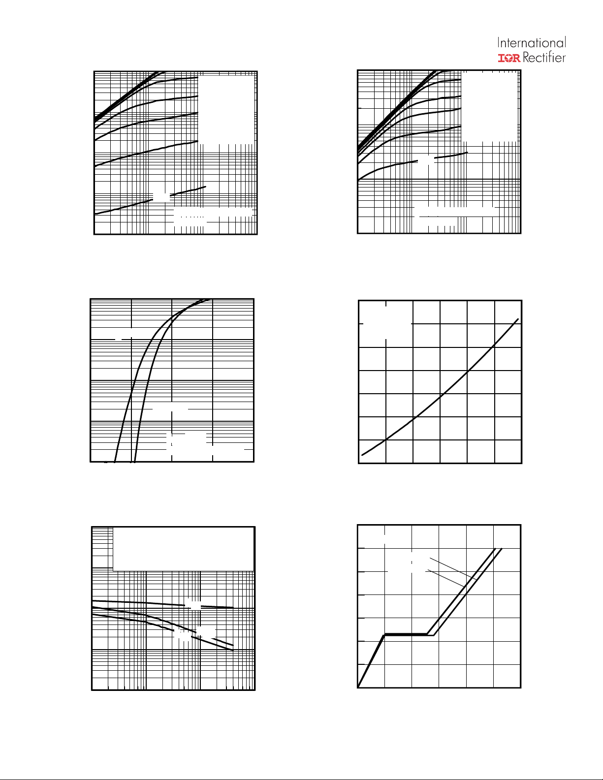
Fig 3. Typical Output Characteristics
TJ = 175°C
TJ = 25°C
1
V
= 10V
DS
≤
60μs PULSE WIDTH
2 4 6 8 10
VGS, Gate-to-Source Voltage (V)
Fig 5. Typical Transfer Characteristics
V
= 0V, f = 1 MHZ
GS
C
= C
C
C
iss
rss
oss
= C
= C
+ Cgd, C
gs
gd
+ C
ds
SHORTED
ds
gd
C
iss
C
ossC
rss
VGS
10V
8.0V
7.0V
6.0V
5.5V
5.0V
1000
VGS
10V
8.0V
7.0V
6.0V
5.5V
5.0V
)
A
(
t
n
e
r
r
u
C
e
c
r
u
o
S
o
t
n
i
a
r
D
,
I
100
D
10
4.5V
60μs
≤
TOP 15V
BOTTOM 4.5V
PULSE WIDTH
Tj = 175°C
1
0.1 1 10 100
VDS, Drain-to-Source Voltage (V)
Fig 4. Typical Output Characteristics
2.0
e
c
n
a
t
s
i
s
e
R
n
O
e
)
c
d
r
e
u
z
i
o
l
S
a
m
o
t
r
-
o
n
i
N
(
a
r
D
,
)
n
o
(
S
D
R
1.8
1.6
1.4
1.2
1.0
0.8
ID = 100A
V
= 10V
GS
0.6
-60 -20 20 60 100 140 180
TJ , Junction Temperature (°C)
Fig 6. Normalized On-Resistance vs. Temperature
14.0
ID= 100A
12.0
)
V
(
e
g
10.0
a
t
l
o
V
e
8.0
c
r
u
o
S
-
6.0
o
t
e
t
a
4.0
G
,
S
G
V
2.0
VDS= 32V
VDS= 20V
100
0.1 1 10 100
VDS, Drain-to-Source Voltage (V)
0.0
0 50 100 150 200 250 300
QG, Total Gate Charge (nC)
Fig 8. Typical Gate Charge vs. Gate-to-Source VoltageFig 7. Typical Capacitance vs. Drain-to-Source Voltage
4 www.irf.com
Page 5
IRFB7434PbF
1000
)
A
(
t
100
n
e
r
r
u
C
n
i
a
r
D
e
s
r
e
v
e
R
,
D
S
I
TJ = 175°C
10
1
0.1
0.0 0.5 1.0 1.5 2.0 2.5
VSD, Source-to-Drain Voltage (V)
TJ = 25°C
V
GS
= 0V
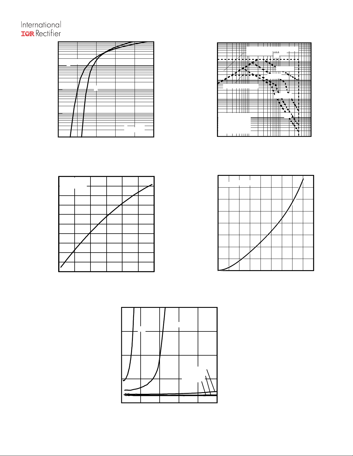
Fig 9. Typical Source-Drain Diode
)
V
(
50
e
g
a
49
t
l
o
V
48
n
w
o
47
d
k
a
e
r
46
B
e
c
45
r
u
o
S
44
o
t
n
43
i
a
r
D
42
,
S
S
41
D
)
R
40
B
(
V
-60 -20 20 60 100 140 180
Forward Voltage
Id = 5.0mA
TJ , Temperature ( °C )
Fig 11. Drain-to-Source Breakdown Voltage
)
20.0
Ω
m
(
e
c
n
a
t
s
i
s
e
R
n
O
e
c
r
u
o
S
o
t
n
i
a
r
D
,
)
n
o
(
S
D
R
15.0
10.0
5.0
0.0
V
0 100 200 300 400 500
= 5.5V
GS
ID, Drain Current (A)
V
GS
= 6.0V
VGS = 7.0V
VGS = 8.0V
VGS = 10V
10000
OPERATION IN THIS AREA
)
A
1000
(
t
n
e
r
r
u
C
100
e
c
r
u
o
S
o
t
n
i
a
r
D
,
D
I
Limited By Package
10
1
Tc = 25°C
Tj = 175°C
Single Pulse
0.1
0.1 1 10 100
VDS, Drain-to-Source Voltage (V)
LIMITED BY RDS(on)
100μsec
1msec
10msec
Fig 10. Maximum Safe Operating Area
1.6
VDS= 0V to 32V
1.4
1.2
1.0
)
J
μ
(
y
0.8
g
r
e
n
E
0.6
0.4
0.2
0.0
0 5 10 15 20 25 30 35 40 45
V
Drain-to-Source Voltage (V)
DS,
Fig 12. Typical C
Stored Energy
OSS
DC
Fig 13. Typical On-Resistance vs. Drain Current
www.irf.com 5
Page 6
IRFB7434PbF
1
W
/
C
°
)
C
J
h
t
Z
(
e
0.01
s
n
o
p
s
e
R
l
a
0.001
m
r
e
h
T
0.1
D = 0.50
0.20
0.10
0.05
0.02
0.01
SINGLE PULSE
( THERMAL RESPONSE )
Notes:
1. Duty Factor D = t1/t2
2. Peak Tj = P dm x Zthjc + Tc
0.0001
1E-006 1E-005 0.0001 0.001 0.01 0.1
t1 , Rectangular Pulse Duration (sec)
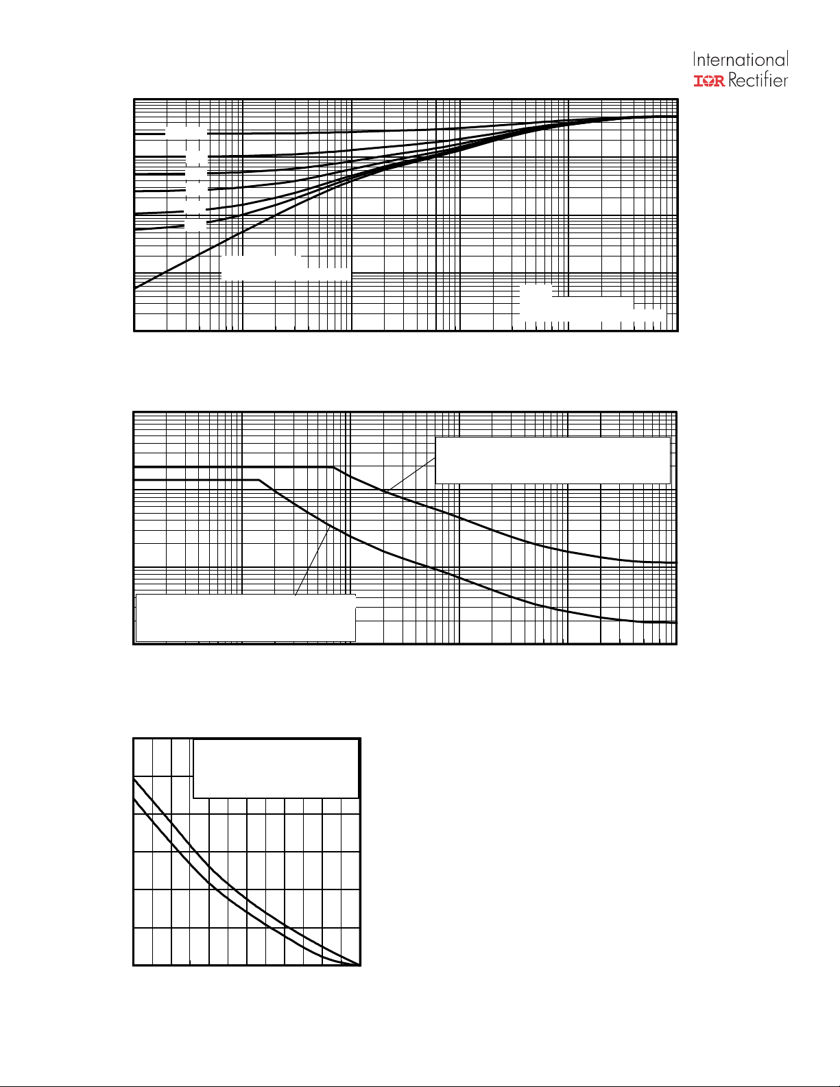
Fig 13. Maximum Effective Transient Thermal Impedance, Junction-to-Case
1000
Allowed avalanche Current vs avalanche
pulsewidth, tav, assuming Δ Tj = 150°C and
)
A
(
100
t
n
e
r
r
u
C
e
h
c
n
a
l
10
a
v
A
Allowed avalanche Current vs avalanche
pulsewidth, tav, assuming ΔΤ j = 25°C and
Tstart = 150°C.
1
1.0E-06 1.0E-05 1.0E-04 1.0E-03 1.0E-02 1.0E-01
tav (sec)
Tstart =25°C (Single Pulse)
Fig 14. Typical Avalanche Current vs.Pulsewidth
600
TOP Single Pulse
500
)
J
m
(
y
g
400
r
e
n
E
e
h
300
c
n
a
l
a
v
A
200
,
R
A
E
100
BOTTOM 1.0% Duty Cycle
ID = 100A
0
25 50 75 100 125 150 175
Starting TJ , Junction Temperature (°C)
Notes on Repetitive Avalanche Curves , Figures 14, 15:
(For further info, see AN-1005 at www.irf.com)
1. Avalanche failures assumption:
Purely a thermal phenomenon and failure occurs at a temperature far in
excess of T
2. Safe operation in Avalanche is allowed as long asT
. This is validated for every part type.
jmax
is not exceeded.
jmax
3. Equation below based on circuit and waveforms shown in Figures 22a, 22b.
4. P
= Average power dissipation per single avalanche pulse.
D (ave)
5. BV = Rated breakdown voltage (1.3 factor accounts for voltage increase
during avalanche).
6. I
= Allowable avalanche current.
av
7. ΔT = Allowable rise in junction temperature, not to exceed T
(assumed as
jmax
25°C in Figure 14, 15).
t
Average time in avalanche.
av =
D = Duty cycle in avalanche = t
Z
(D, tav) = Transient thermal resistance, see Figures 13)
thJC
P
D (ave)
·f
av
= 1/2 ( 1.3·BV·Iav) = DT/ Z
I
2DT/ [1.3·BV·Zth]
av =
E
= P
AS (AR)
D (ave)·tav
thJC
Fig 15. Maximum Avalanche Energy vs. Temperature
6 www.irf.com
Page 7
IRFB7434PbF
4.5
)
V
(
e
g
3.5
a
t
l
o
V
d
l
o
h
s
e
2.5
r
h
t
e
t
a
G
,
)
h
t
(
S
G
V
ID = 250μA
ID = 1.0mA
ID = 1.0A
1.5
0.5
-75 -25 25 75 125 175 225
TJ , Temperature ( °C )
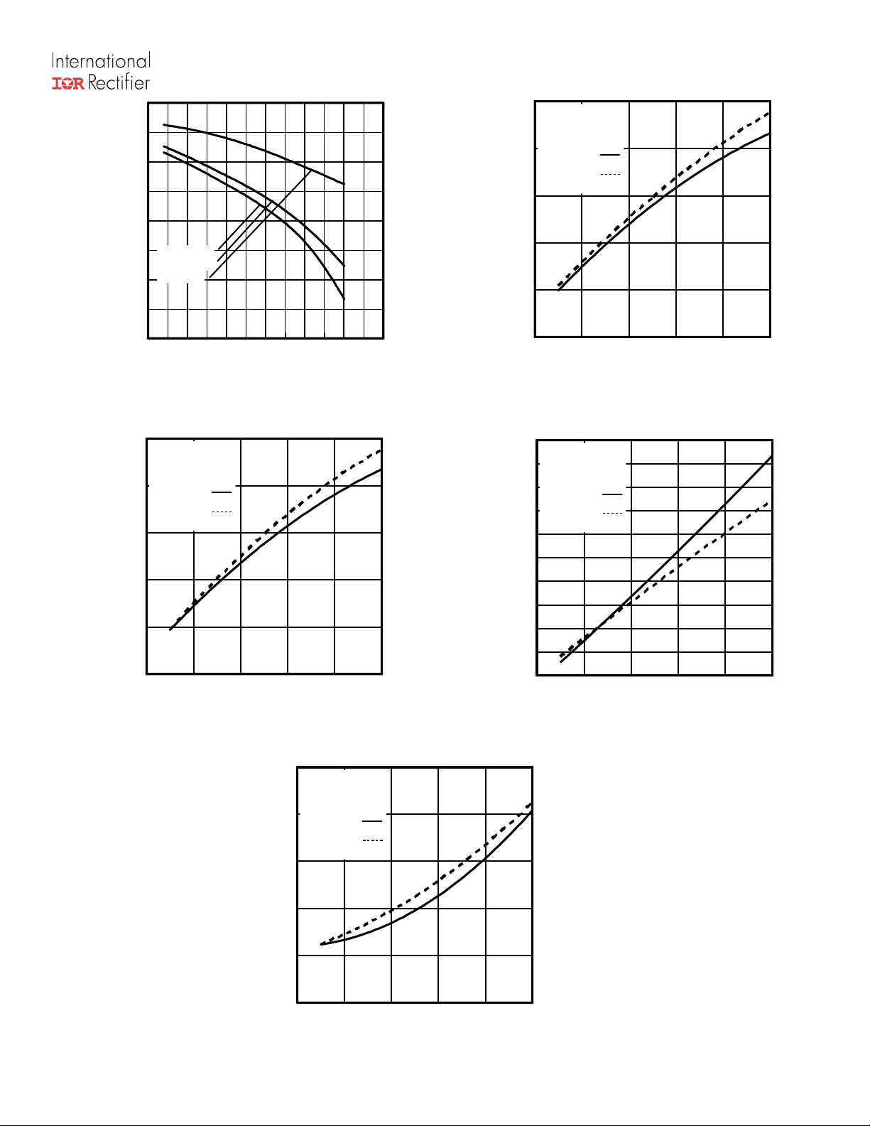
Fig 16. Threshold Voltage vs. Temperature
10
IF = 100A
VR = 34V
8
TJ = 25°C
TJ = 125°C
)
6
A
(
M
R
R
I
4
2
0
0 200 400 600 800 1000
diF /dt (A/μs)
10
IF = 60A
VR = 34V
8
TJ = 25°C
TJ = 125°C
)
6
A
(
M
R
R
I
4
2
0
0 200 400 600 800 1000
diF /dt (A/μs)
Fig. 17 - Typical Recovery Current vs. dif/dt
240
IF = 60A
220
VR = 34V
200
TJ = 25°C
180
TJ = 125°C
)
160
C
n
(
140
R
R
Q
120
100
80
60
40
0 200 400 600 800 1000
diF /dt (A/μs)
Fig. 19 - Typical Stored Charge vs. dif/dtFig. 18 - Typical Recovery Current vs. dif/dt
200
IF = 100A
VR = 34V
160
TJ = 25°C
TJ = 125°C
)
120
C
n
(
R
R
Q
80
40
0
0 200 400 600 800 1000
diF /dt (A/μs)
Fig. 20 - Typical Stored Charge vs. dif/dt
www.irf.com 7
Page 8
IRFB7434PbF
A
V
DS
90%
10%
V
GS
t
d(on)tr
t
d(off)tf
Reverse
Recovery
Current
Driver Gate Drive
P.W.
D.U.T. ISDWaveform
D.U.T. VDSWaveform
Inductor Current
Inductor Curent
* V
GS
D.U.T
+
-
R
G
+
Circuit Layout Considerations
• Low Stray Inductance
• Ground Plane
-
• Low Leakage Inductance
Current Transformer
-
• dv/dt controlled by R
• Driver same type as D.U.T.
• I
controlled by Duty Factor "D"
SD
• D.U.T. - Device Under Test
G
+
V
DD
Re-Applied
Voltage
+
-
Period
Body Diode Forward
Current
di/dt
Diode Recovery
dv/dt
Body Diode Forward Drop
Ripple ≤ 5%
= 5V for Logic Level Devices
D =
P. W .
Period
VGS=10V
V
DD
I
SD
*
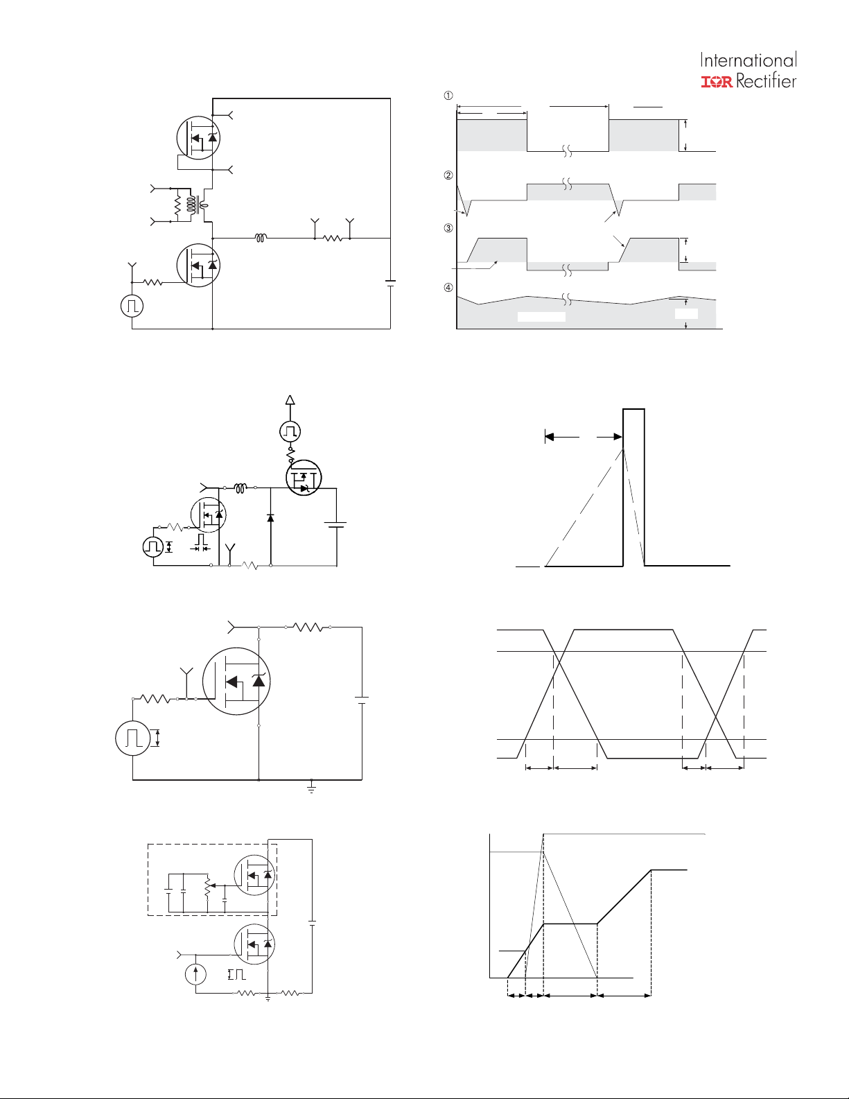
Fig 21. Peak Diode Recovery dv/dt Test Circuit for N-Channel
HEXFET® Power MOSFETs
V
15V
V
DS
L
DRIVER
t
p
(BR)DSS
R
G
20V
V
GS
Fig 22a. Unclamped Inductive Test Circuit
V
GS
R
G
10V
V
GS
Pulse Width ≤ 1 µs
Duty Factor ≤ 0.1 %
D.U.T
I
AS
Ω
0.01
t
p
+
V
DD
-
I
AS
Fig 22b. Unclamped Inductive Waveforms
R
D.U.T.
D
+
V
DD
-
V
DS
Fig 23a. Switching Time Test Circuit Fig 23b. Switching Time Waveforms
Current Regulator
Same Type as D.U.T.
.2μF
12V
V
GS
50KΩ
3mA
.3μF
D.U.T.
+
V
DS
-
Vds
Vgs(th)
Id
Vgs
I
Current Sampling Resistors
Fig 24a. Gate Charge Test Circuit
8 www.irf.com
I
G
D
Qgs1
Qgs2 Qgd Qgodr
Fig 24b. Gate Charge Waveform
Page 9
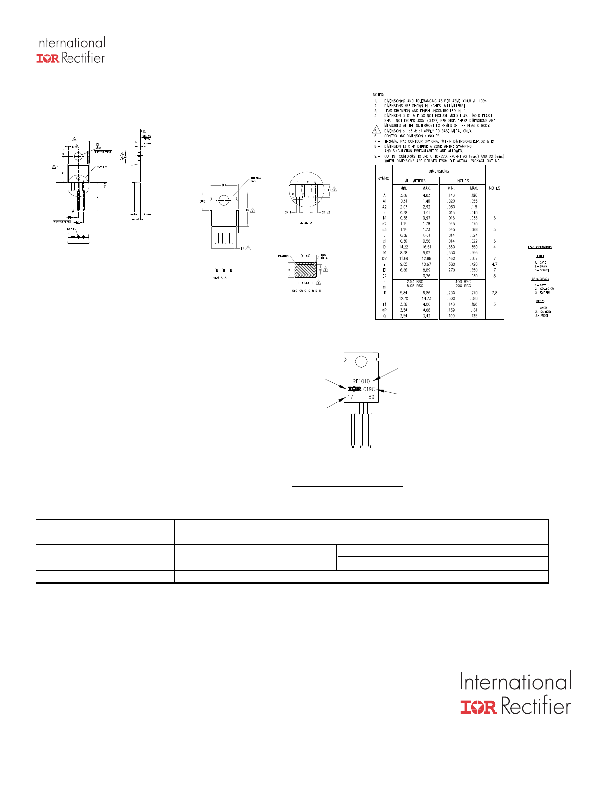
TO-220AB Package Outline
Indust rial
Dimensions are shown in millimeters (inches)
TO-220AB Part Marking Information
IRFB7434PbF
EXAMPL E: THIS IS AN IRF 1010
Note: "P" in assembly line position
LOT CODE 1789
ASS EMBLED ON WW 19, 2000
IN THE ASSEMBLY LINE "C"
indicates "L ead - F r ee"
INTE RNATIONAL
RECTIFIER
LOGO
AS S E MB L Y
LOT CODE
PART NUMBER
DAT E CODE
YEAR 0 = 2000
WEEK 19
LINE C
TO-220AB packages are not recommended for Surface Mount Application.
Note: For the most current drawing please refer to IR website at: http://www.irf.com/package/
Qualification information
Qualification level
RoHS compliant
†
††
†††
(per JEDEC JESD47F
TO-220ABMoisture Sensitivity Level
guidelines)
N/A
(per JE DE C J-S T D-020D
†††
)
Yes
Qualification standards can be found at International Rectifiers web site: http://www.irf.com/product-info/reliability/
Higher qualification ratings may be available should the user have such requirements. Please contact your
Inte rn ati onal Rectifier sales representative for further information: http:www.irf.com/whoto-call/salesrep/
Applicable version of JEDEC standard at the time of product release.
Data and specifications subject to change without notice.
IR WORLD HEADQUARTERS: 101N Sepulveda., El Segundo, California 90245, USA Tel: (310) 252-7105
TAC Fax: (310) 252-7903
Visit us at www.irf.com for sales contact information. 04/2012
www.irf.com 9
 Loading...