

Page 1
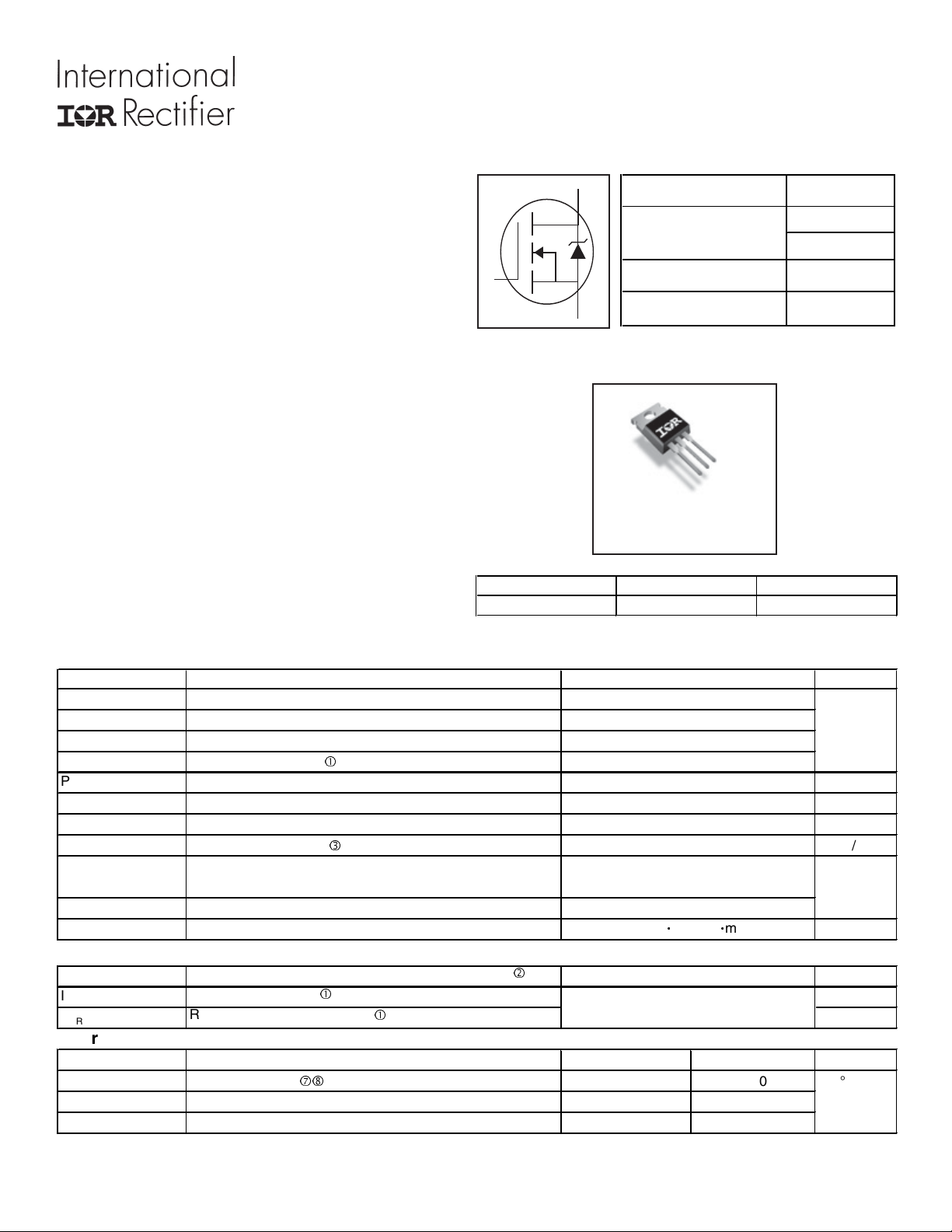
PD - 97727
R
DS(on)
typ.
2.7m
Ω
Ω
Symbol
Parameter
Units
ID @ TC = 25°C
ID @ TC = 100°C
ID @ TC = 25°C
Continuous Drain Current, V
@ 10V (Package Limited)
I
PD @TC = 25°C
V
T
T
EASSingle Pulse Avalanche Energy (Thermally Limited)
d
IARAvalanche Current
c
EARRepetitive Avalanche Energy
c
Thermal Resistance
R
R
R
Max.
IRFB3256PbF
HEXFET® Power MOSFET
D
V
DSS
60V
Applications
l High Efficiency Synchronous Rectification in SMPS
l Uninterruptible Power Supply
l High Speed Power Switching
l Hard Switched and High Frequency Circuits
Benefits
l Improved Gate, Avalanche and Dynamic dV/dt
Ruggedness
l Fully Characterized Capacitance and Avalanche
SOA
l Enhanced body diode dV/dt and dI/dt Capability
l Lead-Free
Absolute Maximum Ratings
max.
G
GDS
Gate Drain Source
I
D (Silicon Limited)
I
S
D
(Package Limited)
D
S
D
G
TO-220AB
3.4m
206A
75A
DM
GS
dv/dt
J
STG
Continuous Drain Current, V
Continuous Drain Current, V
Pulsed Drain Current
Maximum Power Dissipation
Linear Derating Factor
Gate-to-Source Voltage
Peak Diode Recovery
Operating Junction and
Storage Temperature Range
Soldering Temperature, for 10 seconds
Mounting torque, 6-32 or M3 screw
c
e
@ 10V (Silicon Limited)
GS
@ 10V (Silicon Limited)
GS
GS
206
172
75
820
300
2.0
± 20
3.3
-55 to + 175
300 (1.6mm from case)
10lbf
in (1.1Nxm)
x
Avalanche Characteristics
340
See Fig. 14, 15, 22a, 22b
Symbol Parameter Typ. Max. Units
θ
JC
θ
CS
θJA
Junction-to-Case
Case-to-Sink, Flat Greased Surface
Junction-to-Ambient
ij
–––
0.50 –––
––– 62
0.50 °C/W
A
W
W/°C
V
V/ns
°C
mJ
A
mJ
www.irf.com 1
09/22/11
Page 2
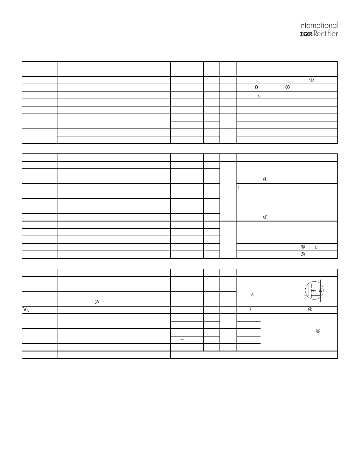
IRFB3256PbF
Symbol
Parameter
Min.
Typ.
Max.
Units
V
Drain-to-Source Breakdown Voltage
60
–––
–––
VΔV
/ΔTJ Breakdown Voltage Temp. Coefficient
–––29–––
mV/°C
R
Static Drain-to-Source On-Resistance
–––
2.7
3.4
Ω
V
Gate Threshold Voltage
2.0
–––
4.0Vgfs
Forward Transconductance
88
–––
–––SRGInternal Gate Resistance
–––
0.79
–––ΩI
Drain-to-Source Leakage Current
–––
–––20μA
–––
–––
250
I
Gate-to-Source Forward Leakage
–––
–––
100nAGate-to-Source Reverse Leakage
–––
–––
-100
Symbol
Parameter
Min.
Typ.
Max.
Units
QgTotal Gate Charge
–––
130
195nCQgsGate-to-Source Charge
–––31–––
QgdGate-to-Drain ("Miller") Charge
–––42–––
Q
Total Gate Charge Sync. (Q
- Qgd)
–––88–––
t
Turn-On Delay Time
–––22–––nstrRise Time
–––77–––
t
Turn-Off Delay Time
–––55–––
tfFall Time
–––64–––
C
Input Capacitance
–––
6600
–––pFC
Output Capacitance
–––
720
–––
C
Reverse Transfer Capacitance
–––
400
–––
C
eff. (ER)
–––
1080
–––
C
eff. (TR)
–––
1400
–––
Symbol
Parameter
Min.
Typ.
Max.
Units
ISContinuous Source Current
–––
–––
A
ISMPulsed Source Current
–––
–––
820A(Body Diode)
VSDDiode Forward Voltage
–––
–––
1.3VtrrReverse Recovery Time
–––43–––nsTJ = 25°C
VR = 51V,
–––53–––
TJ = 125°C
IF = 75A
QrrReverse Recovery Charge
–––58–––nCTJ = 25°C
di/dt = 100A/μs
f
–––65–––
TJ = 125°C
I
Reverse Recovery Current
–––
2.4
–––ATJ = 25°C
tonForward Turn-On Time
Intrinsic turn-on time is negligible (turn-on is dominated by LS+LD)
Conditions
Conditions
Ω
Static @ TJ = 25°C (unless otherwise specified)
(BR)DSS
(BR)DSS
DS(on)
GS(th)
DSS
GSS
Dynamic @ TJ = 25°C (unless otherwise specified)
sync
d(on)
d(off)
iss
oss
rss
oss
oss
Effective Output Capacitance (Energy Related)
Effective Output Capacitance (Time Related)
g
Diode Characteristics
VGS = 0V, ID = 250μA
Reference to 25°C, I
VGS = 10V, ID = 75A
m
VDS = VGS, ID = 150μA
= 25V, ID = 75A
V
DS
= 60V, VGS = 0V
V
DS
V
= 60V, VGS = 0V, TJ = 125°C
DS
= 20V
V
GS
V
= -20V
GS
ID = 75A
= 30V
V
DS
VGS = 10V
= 75A, VDS =0V, VGS = 10V
I
D
f
VDD = 39V
I
= 75A
D
R
= 2.7
G
VGS = 10V
f
VGS = 0V
V
= 48V
DS
ƒ = 1.0 MHz, See Fig. 5
V
= 0V, VDS = 0V to 48V h, See Fig. 11
GS
V
= 0V, VDS = 0V to 48V
GS
= 1.0mA
D
f
Conditions
c
g
MOSFET symbol
showing the
integral reverse
G
p-n junction diode.
TJ = 25°C, IS = 75A, VGS = 0V
.
DSS
f
(Body Diode)
d
RRM
Notes:
Repetitive rating; pulse width limited by max. junction
temperature.
Limited by T
RG = 50Ω, I
above this value.
I
≤ 75A, di/dt ≤ 890A/μs, V
SD
, starting TJ = 25°C, L = 0.12mH
Jmax
= 75A, VGS =10V. Part not recommended for use
AS
DD
≤ V
(BR)DSS
, TJ ≤ 175°C.
206
C
eff. (ER) is a fixed capacitance that gives the same energy as
oss
C
while V
oss
R
is measured at TJ approximately 90°C.
θ
R
value shown is at time zero.
θJC
is rising from 0 to 80% V
DS
Pulse width ≤ 400μs; duty cycle ≤ 2%.
C
eff. (TR) is a fixed capacitance that gives the same charging
oss
time as C
oss
while V
is rising from 0 to 80% V
DS
DSS
.
2 www.irf.com
D
S
Page 3
IRFB3256PbF
1000
TOP 15V
)
A
(
t
n
e
r
100
r
u
C
e
c
r
u
o
S
o
t
n
i
a
r
D
,
D
I
BOTTOM 4.25V
10
VGS
12V
10V
6.0V
5.0V
4.75V
4.50V
4.25V
60μs PULSE WIDTH
≤
Tj = 25°C
1
0.01 0.1 1 10 100
VDS, Drain-to-Source Voltage (V)
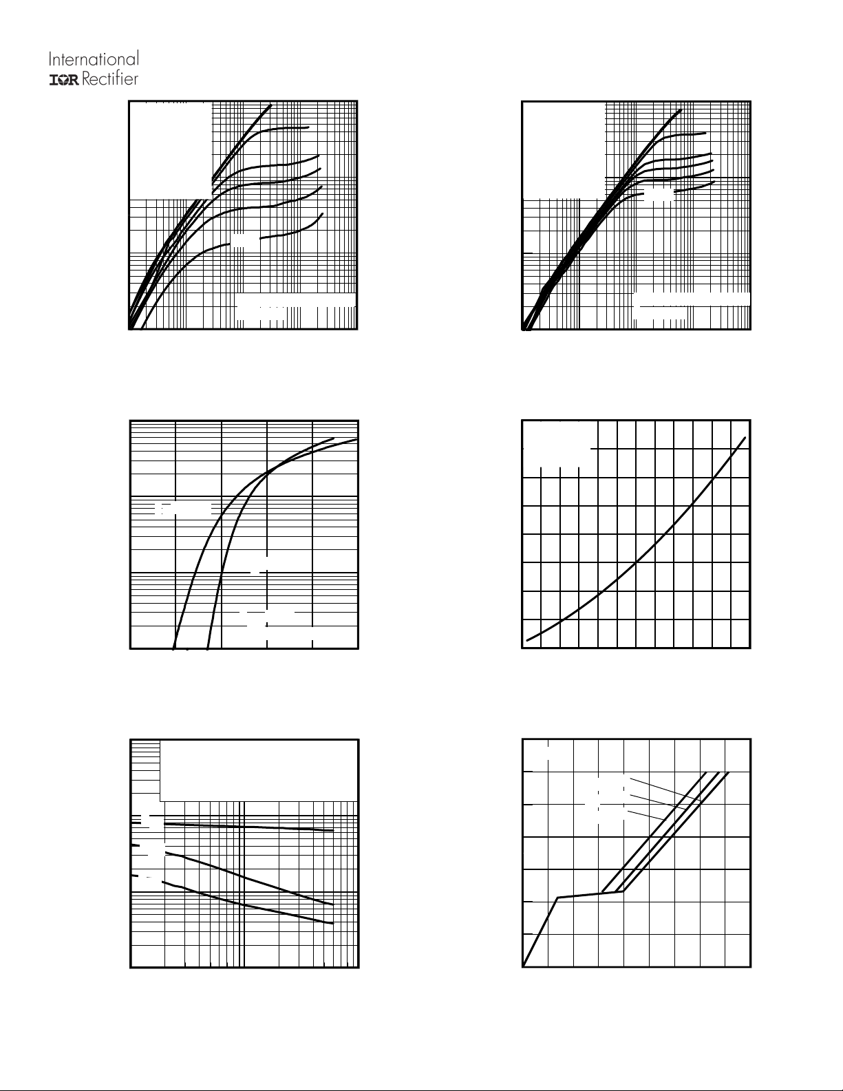
Fig 1. Typical Output Characteristics
1000
)
A
(
t
n
e
r
100
r
u
C
e
c
r
u
o
S
o
t
n
10
i
a
r
D
,
D
I
TJ = 175°C
TJ = 25°C
V
= 25V
DS
≤
60μs PULSE WIDTH
1.0
2 3 4 5 6 7
VGS, Gate-to-Source Voltage (V)
Fig 3. Typical Transfer Characteristics
1000
VGS
12V
10V
6.0V
5.0V
4.75V
4.50V
4.25V
60μs PULSE WIDTH
≤
)
A
(
t
n
e
r
r
u
C
e
c
r
u
o
S
o
t
n
i
a
r
D
,
I
100
10
D
TOP 15V
BOTTOM 4.25V
Tj = 175°C
1
0.01 0.1 1 10 100
VDS, Drain-to-Source Voltage (V)
Fig 2. Typical Output Characteristics
2.2
e
c
n
a
t
s
i
s
e
R
n
O
e
c
r
u
o
S
o
t
n
i
a
r
D
,
)
n
o
(
S
D
R
ID = 75A
2.0
V
= 10V
GS
1.8
1.6
)
d
e
z
i
l
1.4
a
m
r
o
1.2
N
(
1.0
0.8
0.6
-60 -40 -20 0 20 40 60 80 100120140160180
TJ , Junction Temperature (°C)
Fig 4. Normalized On-Resistance vs. Temperature
100000
)
F
10000
p
(
e
c
n
a
t
i
c
a
p
a
C
1000
,
C
100
V
= 0V, f = 1 MHZ
GS
C
= C
= C
= C
+ Cgd, C
gs
gd
+ C
ds
iss
C
rss
C
oss
C
iss
C
oss
C
rss
SHORTED
ds
gd
1 10 100
VDS, Drain-to-Source Voltage (V)
14.0
ID= 75A
12.0
)
V
(
e
g
10.0
a
t
l
o
V
e
8.0
c
r
u
o
S
-
6.0
o
t
e
t
a
4.0
G
,
S
G
V
2.0
VDS= 48V
VDS= 30V
VDS= 12V
0.0
0 20 40 60 80 100 120 140 160 180
QG, Total Gate Charge (nC)
Fig 6. Typical Gate Charge vs. Gate-to-Source VoltageFig 5. Typical Capacitance vs. Drain-to-Source Voltage
www.irf.com 3
Page 4
IRFB3256PbF
1000
)
A
(
t
n
e
r
r
u
C
n
i
a
r
D
e
s
r
e
v
e
R
,
D
S
I
TJ = 175°C
100
TJ = 25°C
10
1.0
0.0 0.5 1.0 1.5 2.0 2.5 3.0
VSD, Source-to-Drain Voltage (V)
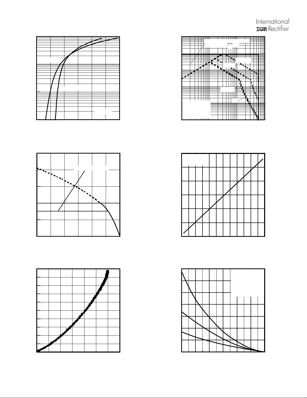
Fig 7. Typical Source-Drain Diode
Forward Voltage
250
200
)
A
(
t
n
150
e
r
r
u
C
n
i
a
r
100
D
,
D
I
50
0
25 50 75 100 125 150 175
TC , Case Temperature (°C)
Limited by package
Fig 9. Maximum Drain Current vs.
V
GS
= 0V
10000
)
A
1000
(
t
n
e
r
r
u
C
100
e
c
r
u
o
S
-
10
o
t
n
i
a
r
D
,
1
D
I
Tc = 25°C
Tj = 175°C
Single Pulse
0.1
0.1 1 10 100
OPERATION IN THIS AREA
LIMITED BY RDS(on)
100μsec
1msec
10msec
DC
VDS, Drain-to-Source Voltage (V)
Fig 8. Maximum Safe Operating Area
)
V
(
72
e
g
a
t
l
o
V
n
w
o
d
k
a
e
r
B
e
c
r
u
o
S
o
t
n
i
a
r
D
,
S
S
D
)
R
B
(
V
ID = 1.0mA
70
68
66
64
62
60
-60 -40 -20 0 20 40 60 80 100120140160180
TJ , Temperature ( °C )
Fig 10. Drain-to-Source Breakdown Voltage
Case Temperature
2.0
1.8
1.6
1.4
)
1.2
J
μ
(
y
1.0
g
r
e
n
0.8
E
0.6
0.4
0.2
0.0
0 10203040506070
V
Drain-to-Source Voltage (V)
DS,
Fig 11. Typical C
Stored Energy
OSS
1400
)
J
m
(
1200
y
g
r
e
n
E
1000
e
h
c
n
800
a
l
a
v
A
e
600
s
l
u
P
e
l
400
g
n
i
S
,
200
S
A
E
0
25 50 75 100 125 150 175
Starting TJ , Junction Temperature (°C)
TOP 12A
BOTTOM75A
I
D
24A
Fig 12. Maximum Avalanche Energy vs. DrainCurrent
4 www.irf.com
Page 5
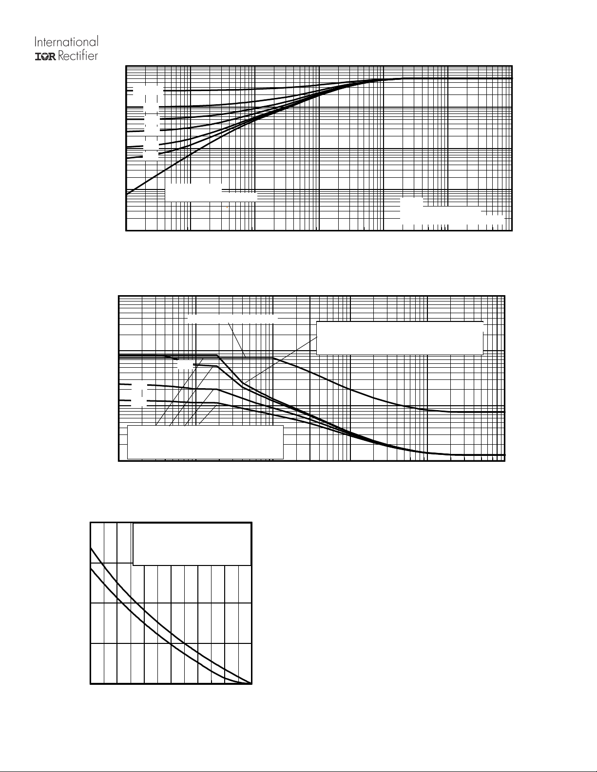
IRFB3256PbF
1
0.1
D = 0.50
0.20
0.10
0.05
0.02
0.01
SINGLE PULSE
( THERMAL RESPONSE )
Notes:
1. Duty Factor D = t1/t2
W
/
C
°
)
Z
(
e
s
n
o
p
s
e
R
l
a
m
r
e
h
T
C
J
h
t
0.001
0.01
2. Peak Tj = P dm x Zthjc + Tc
0.0001
1E-006 1E-005 0.0001 0.001 0.01 0.1 1
t1 , Rectangular Pulse Duration (sec)
Fig 13. Maximum Effective Transient Thermal Impedance, Junction-to-Case
1000
Duty Cycle = Single Pulse
Allowed avalanche Current vs avalanche
)
A
(
100
t
n
e
r
r
u
C
e
h
c
n
a
l
a
v
A
10
0.05
0.10
0.01
pulsewidth, tav, assuming ΔTj = 150°C and
Tstart =25°C (Single Pulse)
Allowed avalanche Current vs avalanche
pulsewidth, tav, assuming ΔΤj = 25°C and
Tstart = 150°C.
1
1.0E-06 1.0E-05 1.0E-04 1.0E-03 1.0E-02 1.0E-01
tav (sec)
Fig 14. Typical Avalanche Current vs.Pulsewidth
400
TOP Single Pulse
BOTTOM 1.0% Duty Cycle
)
J
m
300
(
y
g
r
e
n
E
e
h
200
c
n
a
l
a
v
A
,
R
100
A
E
ID = 75A
0
25 50 75 100 125 150 175
Starting TJ , Junction Temperature (°C)
Notes on Repetitive Avalanche Curves , Figures 14, 15:
(For further info, see AN-1005 at www.irf.com)
1. Avalanche failures assumption:
Purely a thermal phenomenon and failure occurs at a temperature far in
excess of T
2. Safe operation in Avalanche is allowed as long asT
3. Equation below based on circuit and waveforms shown in Figures 16a, 16b.
4. P
D (ave)
5. BV = Rated breakdown voltage (1.3 factor accounts for voltage increase
. This is validated for every part type.
jmax
is not exceeded.
jmax
= Average power dissipation per single avalanche pulse.
during avalanche).
6. I
= Allowable avalanche current.
av
7. ΔT = Allowable rise in junction temperature, not to exceed T
(assumed as
jmax
25°C in Figure 14, 15).
t
Average time in avalanche.
av =
D = Duty cycle in avalanche = t
Z
(D, tav) = Transient thermal resistance, see Figures 13)
thJC
P
D (ave)
·f
av
= 1/2 ( 1.3·BV·Iav) = DT/ Z
I
2DT/ [1.3·BV·Zth]
av =
E
= P
AS (AR)
D (ave)·tav
thJC
Fig 15. Maximum Avalanche Energy vs. Temperature
www.irf.com 5
Page 6
IRFB3256PbF
4.0
)
V
3.5
(
e
g
a
t
l
3.0
o
V
d
l
o
2.5
h
s
e
r
h
t
2.0
e
t
a
G
,
)
h
t
(
S
G
V
ID = 150μA
ID = 1.0mA
1.5
ID = 1.0A
1.0
0.5
-75 -25 25 75 125 175
TJ , Temperature ( °C )
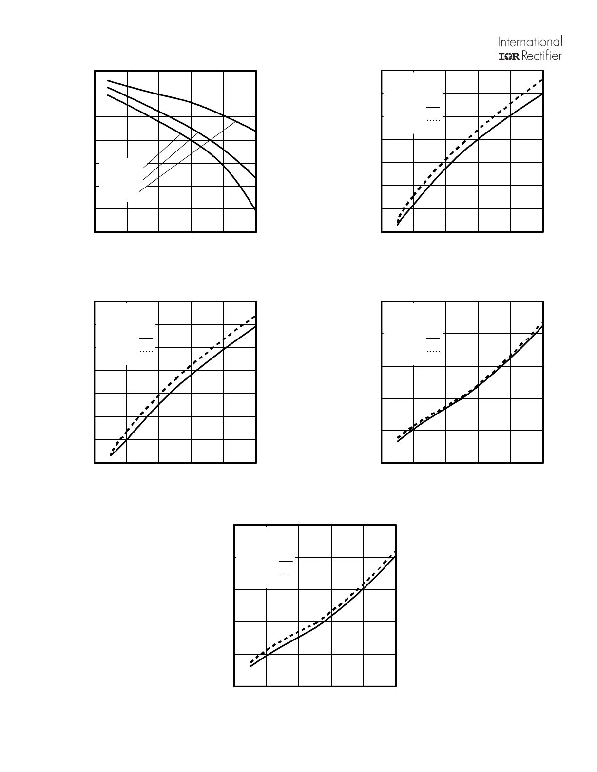
Fig 16. Threshold Voltage vs. Temperature
16
IF = 45A
14
VR = 51V
TJ = 25°C
12
TJ = 125°C
)
10
A
(
M
R
8
R
I
16
IF = 30A
14
VR = 51V
TJ = 25°C
12
TJ = 125°C
)
10
A
(
M
R
8
R
I
6
4
2
0 200 400 600 800 1000
diF /dt (A/μs)
Fig. 17 - Typical Recovery Current vs. dif/dt
500
IF = 30A
VR = 51V
400
TJ = 25°C
TJ = 125°C
)
300
C
n
(
R
R
Q
200
6
4
2
0 200 400 600 800 1000
diF /dt (A/μs)
500
400
)
300
C
n
(
R
R
Q
200
100
0
0 200 400 600 800 1000
100
0
0 200 400 600 800 1000
diF /dt (A/μs)
Fig. 19 - Typical Stored Charge vs. dif/dtFig. 18 - Typical Recovery Current vs. dif/dt
IF = 45A
VR = 51V
TJ = 25°C
TJ = 125°C
diF /dt (A/μs)
Fig. 20 - Typical Stored Charge vs. dif/dt
6 www.irf.com
Page 7
IRFB3256PbF
A
D.U.T
+
-
R
G
+
Circuit Layout Considerations
• Low Stray Inductance
• Ground Plane
-
• Low Leakage Inductance
Current Transformer
-
• dv/dt controlled by R
• Driver same type as D.U.T.
• ISD controlled by Duty Factor "D"
• D.U.T. - Device Under Test
G
Reverse
Recovery
+
-
Current
Re-Applied
Voltage
+
V
DD
Driver Gate Drive
D.U.T. ISDWaveform
D.U.T. VDSWaveform
Inductor Current
Inductor Curent
* V
GS
Period
P.W.
Body Diode Forward
Current
di/dt
Diode Recovery
dv/dt
Body Diode Forward Drop
Ripple ≤ 5%
= 5V for Logic Level Devices
D =
P. W .
Period
VGS=10V
V
DD
I
SD
*
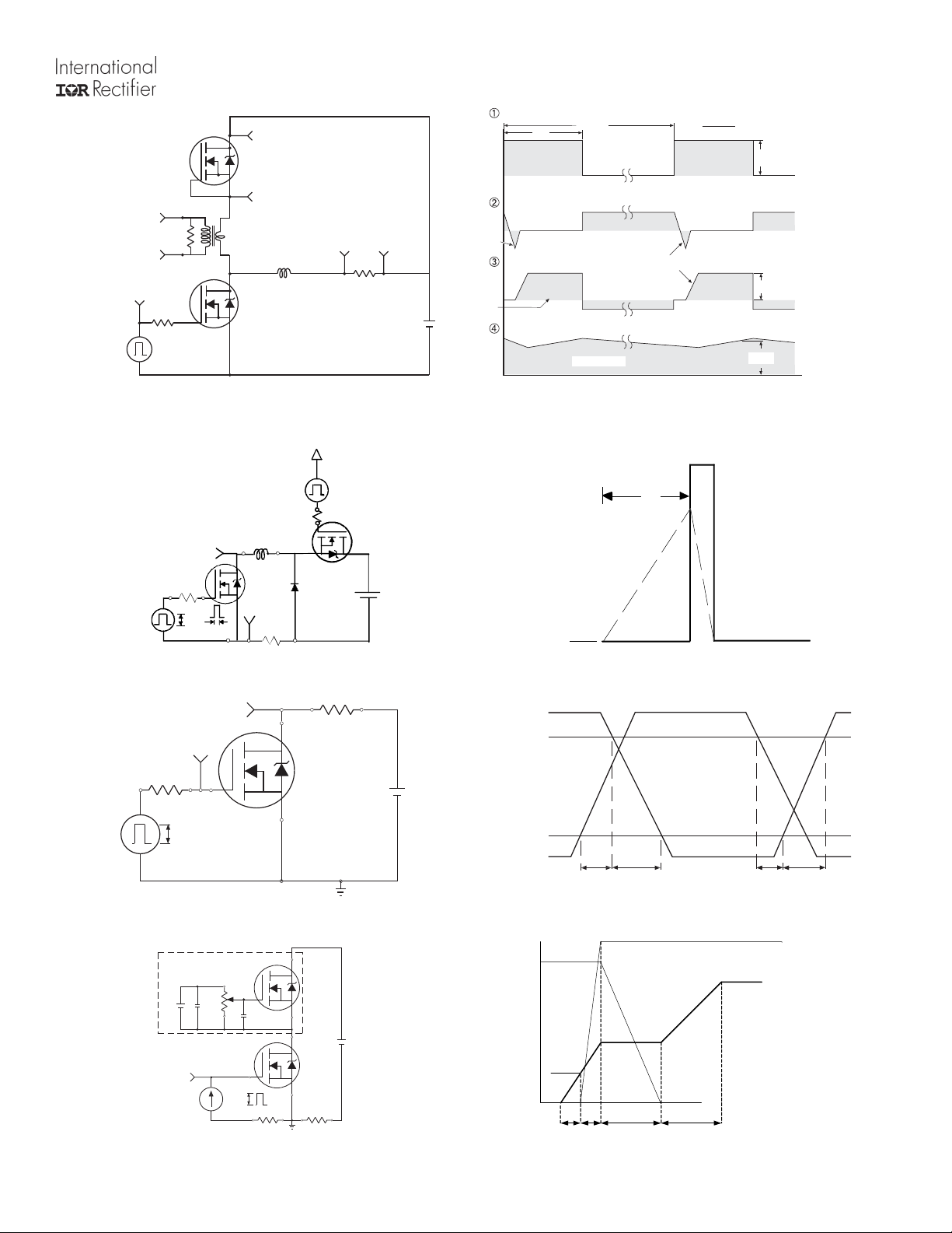
Fig 21. Peak Diode Recovery dv/dt Test Circuit for N-Channel
HEXFET® Power MOSFETs
V
15V
V
DS
L
DRIVER
t
p
(BR)DSS
R
G
V
20V
GS
Fig 22a. Unclamped Inductive Test Circuit
V
GS
R
G
10V
V
GS
Pulse Width ≤ 1 µs
Duty Factor ≤ 0.1 %
D.U.T
I
AS
Ω
0.01
t
p
+
V
DD
-
I
AS
Fig 22b. Unclamped Inductive Waveforms
R
V
DS
D
V
DS
90%
D.U.T.
+
V
DD
-
10%
V
GS
t
d(on)tr
t
d(off)tf
Fig 23a. Switching Time Test Circuit Fig 23b. Switching Time Waveforms
Current Regulator
Same Type as D.U.T.
.2μF
12V
V
GS
50KΩ
3mA
.3μF
D.U.T.
+
V
DS
-
Vds
Vgs(th)
Id
Vgs
I
Current Sampling Resistors
Fig 24a. Gate Charge Test Circuit
www.irf.com 7
I
G
D
Qgs1
Qgs2 Qgd Qgodr
Fig 24b. Gate Charge Waveform
Page 8
IRFB3256PbF
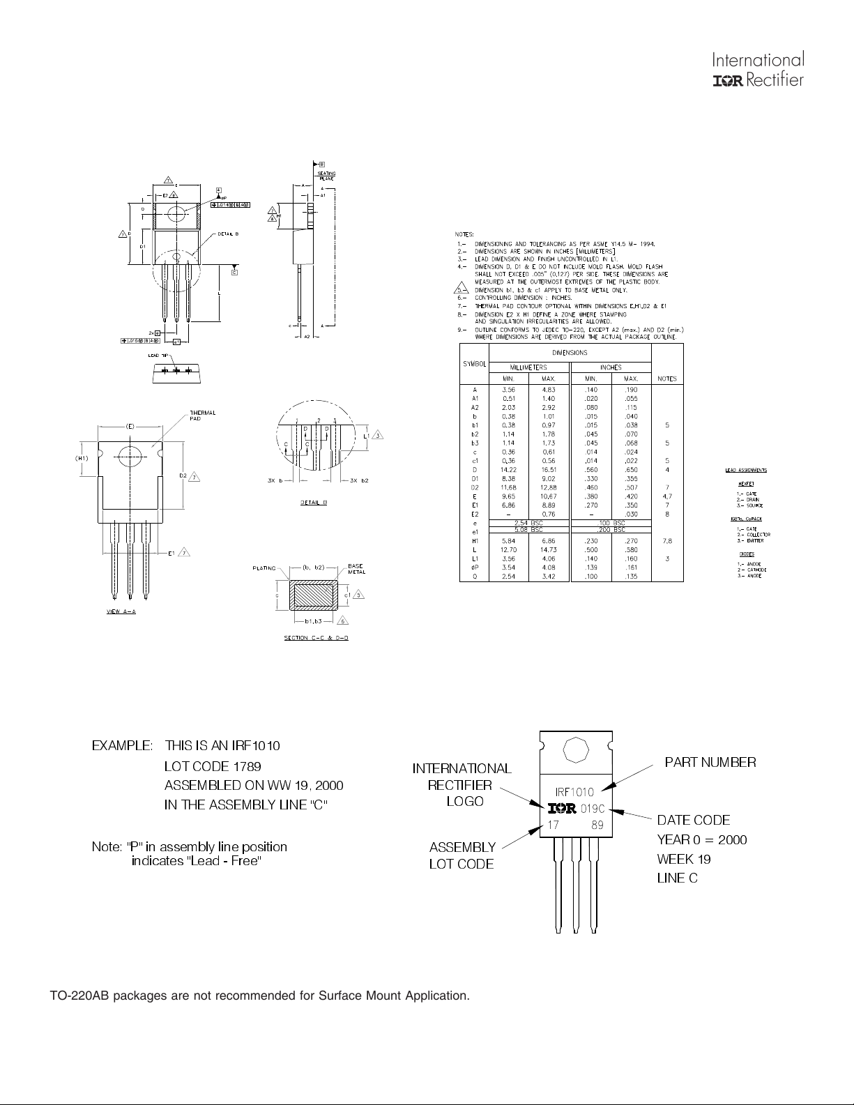
TO-220AB Package Outline
Dimensions are shown in millimeters (inches)
TO-220AB Part Marking Information
(;$03/( 7+,6,6$1,5)
/27&2'(
$66(0%/('21::
,17+($66(0%/</,1(&
1RWH3LQDVVHPEO\OLQHSRVLWLRQ
LQGLFDWHV/HDG)UHH
TO-220AB packages are not recommended for Surface Mount Application.
Note: For the most current drawing please refer to IR website at: http://www.irf.com/package/
,17(51$7,21$/
5(&7,),(5
/2*2
$66(0%/<
/27&2'(
8 www.irf.com
3$57180%(5
'$7(&2'(
<($5
:((.
/,1(&
Page 9
IRFB3256PbF
Qualification information
Qualification level
†
Cons umer
(per JEDE C JES D47F
††
†††
guidelines )
MS L 1
Moisture Sensitivity Level
TSOP-6
(per IP C/JE DE C J- S T D-02 0 D
RoHS compliant Yes
† Qualification standards can be found at International Rectifier’s web site
http://www.irf.com/product-info/reliability
†† Higher qualification ratings may be available should the user have such requirements.
Please contact your International Rectifier sales representative for further information:
http://www.irf.com/whoto-call/salesrep/
††† Applicable version of JEDEC standard at the time of product release.
†††
)
Data and specifications subject to change without notice.
IR WORLD HEADQUARTERS: 101 N. Sepulveda Blvd., El Segundo, California 90245, USA Tel: (310) 252-7105
TAC Fax: (310) 252-7903
Visit us at www.irf.com for sales contact information. 09/2011
www.irf.com 9
 Loading...