

Page 1
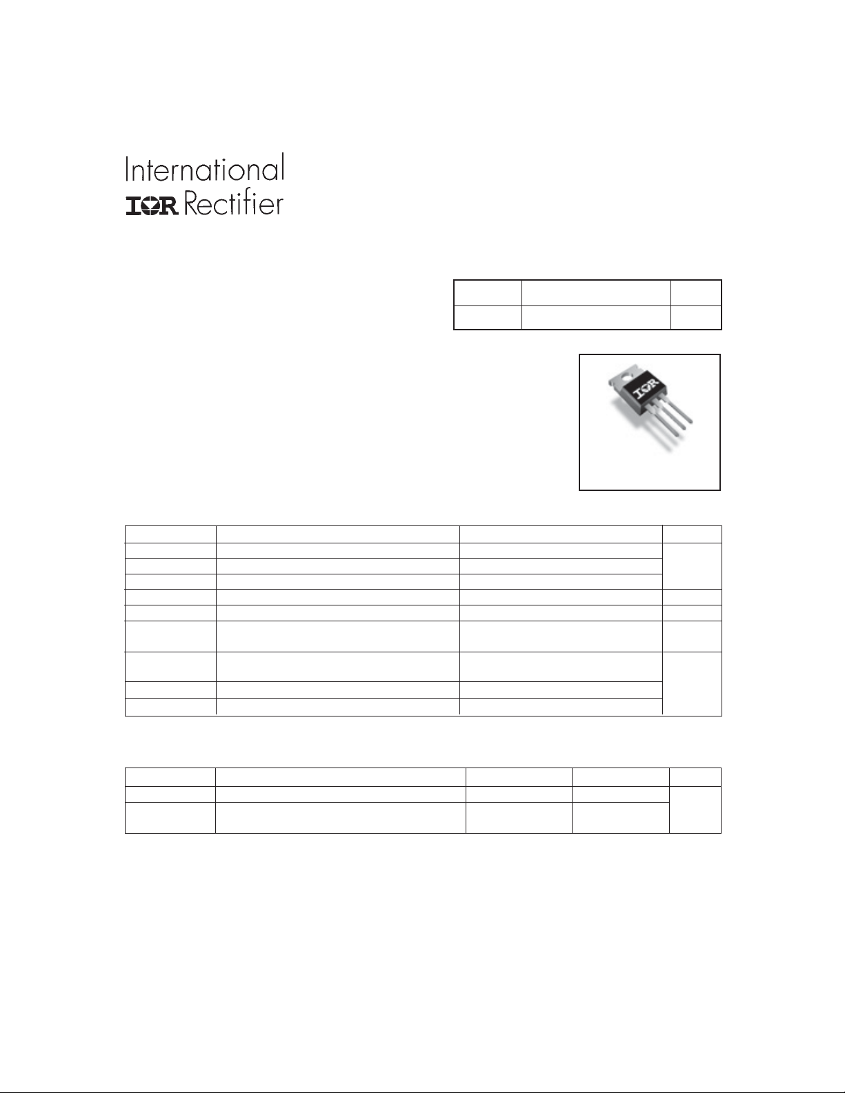
SMPS MOSFET
IRFB260NPbF
PD - 95473
HEXFET® Power MOSFET
Applications
l High frequency DC-DC converters
l Lead-Free
V
DSS
R
DS(on)
max I
200V 0.040Ω 56A
Benefits
l Low Gate-to-Drain Charge to Reduce Switching Losses
l Fully Characterized Capacitance Including Effective C
OSS
to
Simplify Design, (See App. Note AN1001)
l Fully Characterized Avalanche Voltage and Current
TO-220AB
Absolute Maximum Ratings
Parameter Max. Units
ID @ TC = 25°C Continuous Drain Current, VGS @ 10V 56
ID @ TC = 100°C Continuous Drain Current, VGS @ 10V 40 A
I
DM
PD @TC = 25°C Power Dissipation 380 W
V
GS
dv/dt Peak Diode Recovery dv/dt 10 V/ns
T
J
T
STG
Pulsed Drain Current 220
Linear Derating Factor 2.5 W/°C
Gate-to-Source Voltage ± 20 V
Operating Junction and -55 to + 175
Storage Temperature Range
Soldering Temperature, for 10 seconds 300 (1.6mm from case )
Mounting torqe, 6-32 or M3 screw 10 lbf•in (1.1N•m)
D
°C
Thermal Resistance
Parameter Typ. Max. Units
R
θJC
R
θCS
R
θJA
Notes through are on page 8
Junction-to-Case ––– 0.40
Case-to-Sink, Flat, Greased Surface 0.50 ––– °C/W
Junction-to-Ambient ––– 62
www.irf.com 1
7/7/04
Page 2
IRFB260NPbF
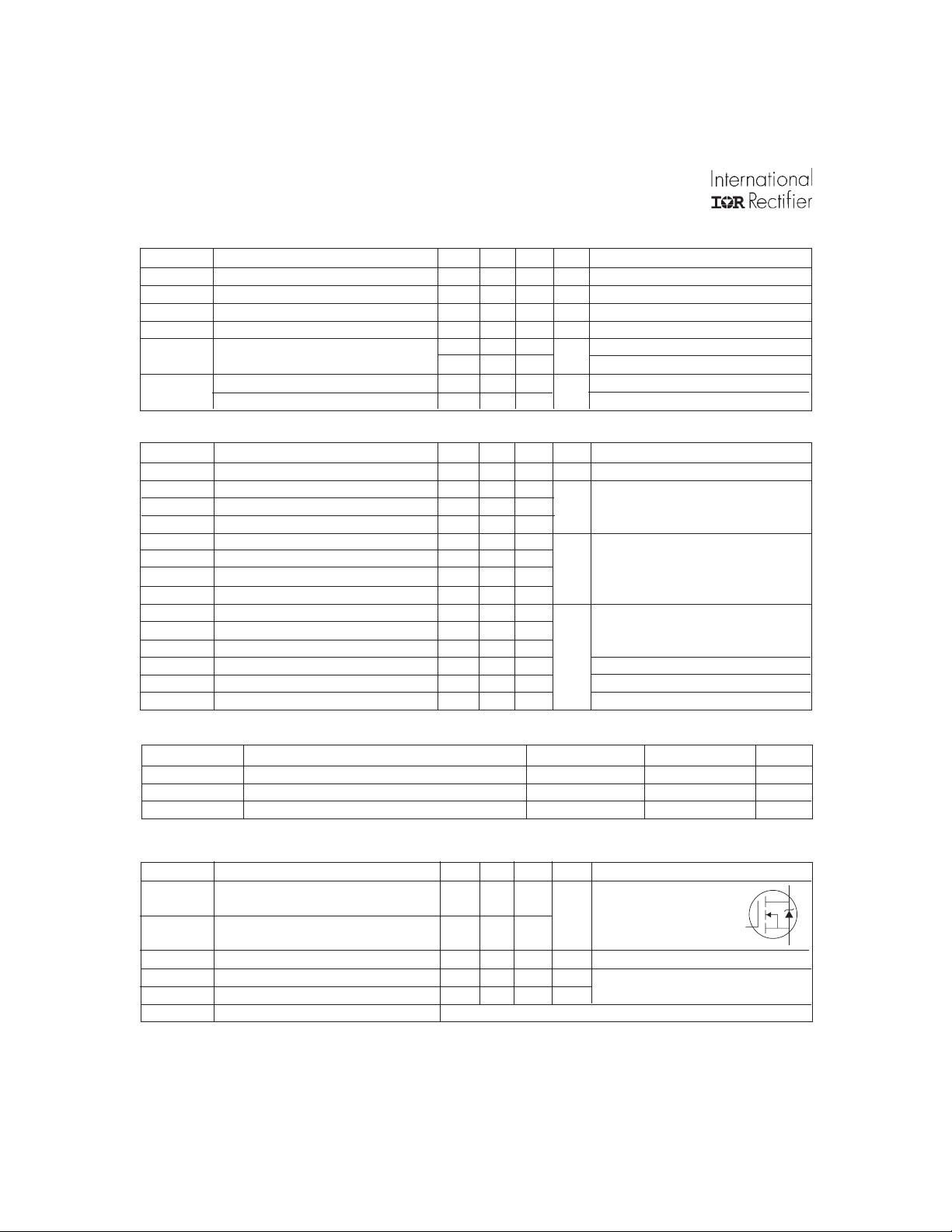
Static @ TJ = 25°C (unless otherwise specified)
Parameter Min. Typ. Max. Units Conditions
V
(BR)DSS
∆V
(BR)DSS
R
DS(on)
V
GS(th)
I
DSS
I
GSS
Dynamic @ TJ = 25°C (unless otherwise specified)
g
fs
Q
g
Q
gs
Q
gd
t
d(on)
t
r
t
d(off)
t
f
C
iss
C
oss
C
rss
C
oss
C
oss
C
eff. Effective Output Capacitance ––– 500 ––– VGS = 0V, VDS = 0V to 160V
oss
Drain-to-Source Breakdown Voltage 200 ––– ––– V VGS = 0V, ID = 250µA
/∆T
Breakdown Voltage Temp. Coefficient
J
––– 0.26 ––– V/°C Reference to 25°C, ID = 1mA
Static Drain-to-Source On-Resistance ––– ––– 0.040 Ω VGS = 10V, ID = 34A
Gate Threshold Voltage 2.0 ––– 4.0 V VDS = VGS, ID = 250µA
Drain-to-Source Leakage Current
––– ––– 25
––– ––– 250 VDS = 160V, VGS = 0V, TJ = 150°C
Gate-to-Source Forward Leakage ––– ––– 100 VGS = 20V
Gate-to-Source Reverse Leakage ––– ––– -100
µA
nA
V
= 200V, VGS = 0V
DS
VGS = -20V
Parameter Min. Typ. Max. Units Conditions
Forward Transconductance 29 ––– ––– S VDS = 50V, ID = 34A
Total Gate Charge ––– 150 220 ID = 34A
Gate-to-Source Charge ––– 24 37 nC VDS = 160V
Gate-to-Drain ("Miller") Charge ––– 67 100 VGS = 10V
Turn-On Delay Time ––– 17 ––– VDD = 100V
Rise Time ––– 64 ––– ID = 34A
Turn-Off Delay Time ––– 52 ––– RG = 1.8Ω
ns
Fall Time ––– 50 ––– VGS = 10V
Input Capacitance ––– 4220 ––– VGS = 0V
Output Capacitance ––– 580 ––– VDS = 25V
Reverse Transfer Capacitance ––– 140 ––– pF ƒ = 1.0MHz
Output Capacitance ––– 5080 ––– VGS = 0V, VDS = 1.0V, ƒ = 1.0MHz
Output Capacitance ––– 230 ––– VGS = 0V, VDS = 160V, ƒ = 1.0MHz
Avalanche Characteristics
Parameter Typ. Max. Units
E
AS
I
AR
E
AR
Single Pulse Avalanche Energy ––– 450 mJ
Avalanche Current ––– 34 A
Repetitive Avalanche Energy ––– 38 mJ
Diode Characteristics
Parameter Min. Typ. Max. Units Conditions
I
S
I
SM
V
SD
t
rr
Q
rr
t
on
Continuous Source Current MOSFET symbol
(Body Diode)
Pulsed Source Current integral reverse
(Body Diode)
––– –––
––– –––
56
220
showing the
A
p-n junction diode.
G
Diode Forward Voltage ––– ––– 1.3 V TJ = 25°C, IS = 34A, VGS = 0V
Reverse Recovery Time ––– 240 360 ns TJ = 25°C, IF = 34A
Reverse RecoveryCharge ––– 2.1 3.2 µC di/dt = 100A/µs
Forward Turn-On Time Intrinsic turn-on time is negligible (turn-on is dominated by LS+LD)
2 www.irf.com
D
S
Page 3
IRFB260NPbF
)
A
(
t
n
e
r
r
u
C
e
c
r
u
o
S
o
t
n
i
a
r
D
,
I
1000
100
10
1
D
VGS
TOP 15V
10V
8.0V
7.0V
6.0V
5.5V
5.0V
BOTTOM 4.5V
4.5V
20µs PULSE WIDTH
Tj = 25°C
0.1
0.1 1 10 100
VDS, Drain-to-Source Voltage (V)
1000.00
)
Α
(
t
n
e
r
r
100.00
u
C
e
c
r
u
o
S
o
t
-
10.00
n
i
a
r
D
,
D
I
1.00
3.0 5.0 7.0 9.0 11.0 13.0 15.0
TJ = 25°C
V
= 15V
DS
20µs PULSE WIDTH
VGS, Gate-to-Source Voltage (V)
TJ = 175°C
)
A
(
t
n
e
r
r
u
C
e
c
r
u
o
S
o
t
n
i
a
r
D
,
I
1000
100
10
1
D
VGS
TOP 15V
10V
8.0V
7.0V
6.0V
5.5V
5.0V
BOTTOM 4.5V
4.5V
20µs PULSE WIDTH
Tj = 175°C
0.1
0.1 1 10 100
VDS, Drain-to-Source Voltage (V)
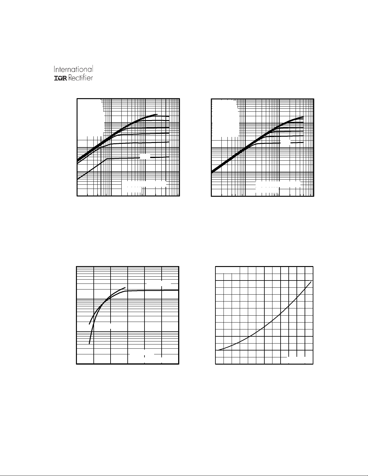
Fig 2. Typical Output CharacteristicsFig 1. Typical Output Characteristics
3.5
56A
I =
D
3.0
2.5
2.0
1.5
(Normalized)
1.0
0.5
DS(on)
R , Drain-to-Source On Resistance
0.0
-60 -40 -20 0 20 40 60 80 100 120 140 160 180
T , Junction Temperature ( C)
J
V =
GS
°
10V
Fig 3. Typical Transfer Characteristics
Fig 4. Normalized On-Resistance
Vs. Temperature
www.irf.com 3
Page 4
IRFB260NPbF
100000
10000
)
F
p
(
e
c
n
a
t
i
1000
c
a
p
a
C
,
C
100
10
1 10 100 1000
V
= 0V, f = 1 MHZ
GS
C
= C
iss
gs
C
= C
rss
gd
C
= C
ds
+ C
oss
Crss
+ Cgd, C
gd
Ciss
Coss
VDS, Drain-to-Source Voltage (V)
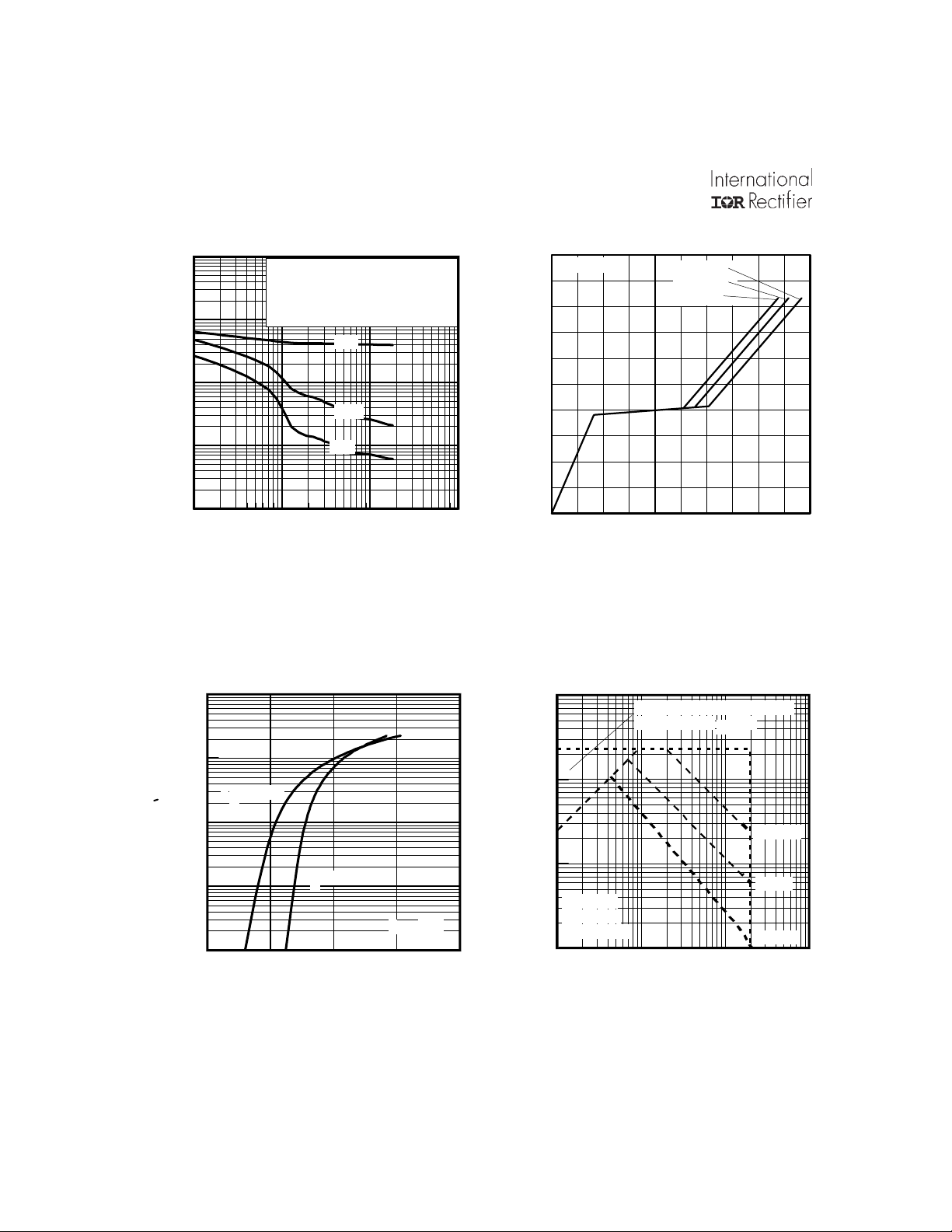
Fig 5. Typical Capacitance Vs.
Drain-to-Source Voltage
1000.00
)
A
(
t
100.00
n
e
r
r
u
C
n
i
a
r
D
e
s
r
e
v
e
R
,
D
S
I
10.00
1.00
0.10
TJ = 175°C
TJ = 25°C
0.0 0.5 1.0 1.5 2.0
VSD, Source-toDrain Voltage (V)
SHORTED
ds
V
GS
= 0V
12
D
I =
34A
10
7
5
2
GS
V , Gate-to-Source Voltage (V)
0
0 30 60 90 120 150
Q , Total Gate Charge (nC)
G
V = 160V
DS
V = 100V
DS
V = 40V
DS
Fig 6. Typical Gate Charge Vs.
Gate-to-Source Voltage
1000
)
A
(
t
n
e
r
r
100
u
C
e
c
r
u
o
S
o
t
n
10
i
a
r
D
,
Tc = 25°C
D
I
Tj = 175°C
Single Pulse
1
1 10 100 1000
OPERATION IN THIS AREA
LIMITED BY RDS(on)
V
, Drain-toSource Voltage (V)
DS
100µsec
1msec
10msec
Fig 7. Typical Source-Drain Diode
Fig 8. Maximum Safe Operating Area
Forward Voltage
4 www.irf.com
Page 5
IRFB260NPbF
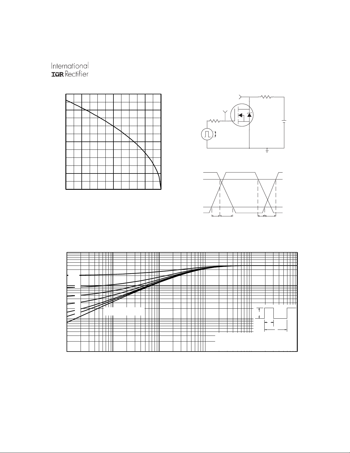
R
D.U.T.
D
+
V
DD
-
60
50
R
40
V
DS
V
GS
G
10V
30
Pulse Width ≤ 1 µs
Duty Factor ≤ 0.1 %
D
I , Drain Current (A)
20
10
Fig 10a. Switching Time Test Circuit
V
DS
90%
0
25 50 75 100 125 150 175
T , Case Temperatur e ( C)
C
°
10%
V
GS
Fig 9. Maximum Drain Current Vs.
t
d(on)tr
t
d(off)tf
Case Temperature
Fig 10b. Switching Time Waveforms
1
D = 0.50
thJC
0.1
0.20
0.10
0.05
0.02
0.01
0.01
Thermal Response (Z )
0.001
0.00001 0.0001 0.001 0.01 0.1 1
SINGLE PULSE
(THERMAL RESPONSE)
t , Rectangular Pulse Duration (sec)
1
P
DM
Not es:
1. Duty factor D = t / t
2. Peak T = P x Z + T
1 2
J DM thJC C
t
1
t
2
Fig 11. Maximum Effective Transient Thermal Impedance, Junction-to-Case
www.irf.com 5
Page 6
IRFB260NPbF
A
15V
DRIVER
+
-
V
R
G
20V
V
DS
t
L
D.U.T
I
AS
0.01
p
Ω
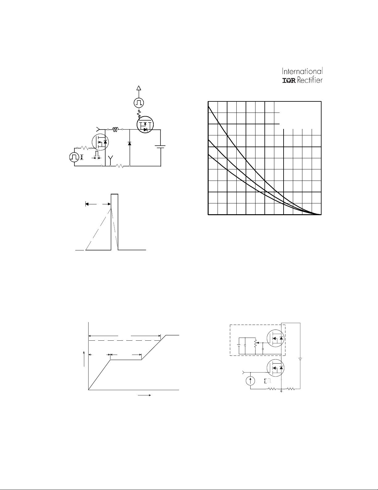
Fig 12a. Unclamped Inductive Test Circuit
V
(BR)DSS
t
p
I
AS
Fig 12b. Unclamped Inductive Waveforms
DD
850
TOP
680
510
340
170
AS
E , Single Pulse Avalanche Energy (mJ)
0
25 50 75 100 125 150 175
Starting T , Junction Temperature ( C)
J
BOTTOM
Fig 12c. Maximum Avalanche Energy
Vs. Drain Current
I
D
14A
24A
34A
°
Current Regulator
Same Type as D.U.T.
Q
G
10 V
Q
GS
V
G
Q
GD
Charge
Fig 13a. Basic Gate Charge Waveform
12V
V
GS
Fig 13b. Gate Charge Test Circuit
50KΩ
.2µF
.3µF
3mA
Current Sampling Resistors
+
V
D.U.T.
I
G
DS
-
I
D
6 www.irf.com
Page 7
IRFB260NPbF
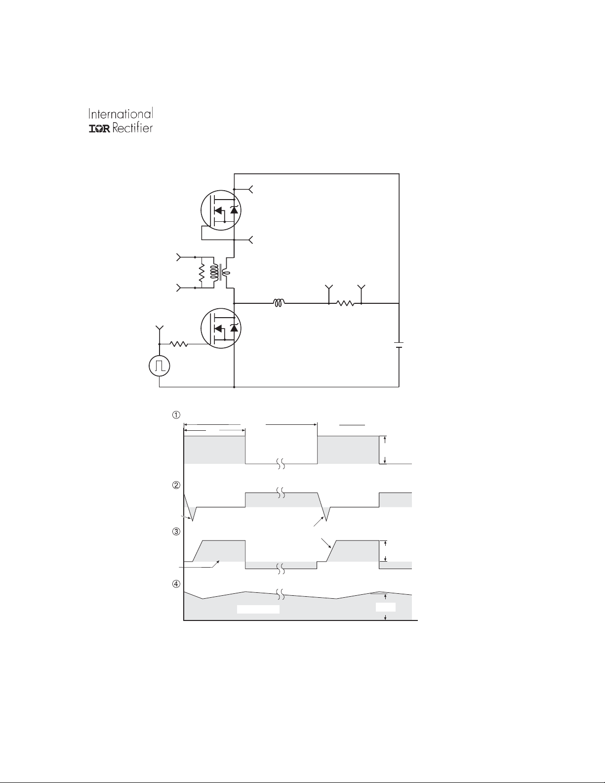
Peak Diode Recovery dv/dt Test Circuit
D.U.T
+
-
R
G
Driver Gate Drive
P.W.
+
Circuit Layout Considerations
• Low Stray Inductance
• Ground Plane
• Low Leakage Inductance
Current Transformer
-
-
• dv/dt controlled by R
• Driver same type as D.U.T.
G
• ISD controlled by Duty Factor "D"
• D.U.T. - Device Under Test
Period
D =
Period
P. W .
+
+
V
DD
-
VGS=10V
*
D.U.T. ISDWaveform
Reverse
Recovery
Current
Re-Applied
Voltage
D.U.T. VDSWaveform
Inductor Curent
* V
= 5V for Logic Level Devices
GS
Body Diode Forward
Current
di/dt
Diode Recovery
dv/dt
Body Diode Forward Drop
Ripple ≤ 5%
V
DD
I
SD
Fig 14. For N-Channel HEXFET® Power MOSFETs
www.irf.com 7
Page 8
IRFB260NPbF
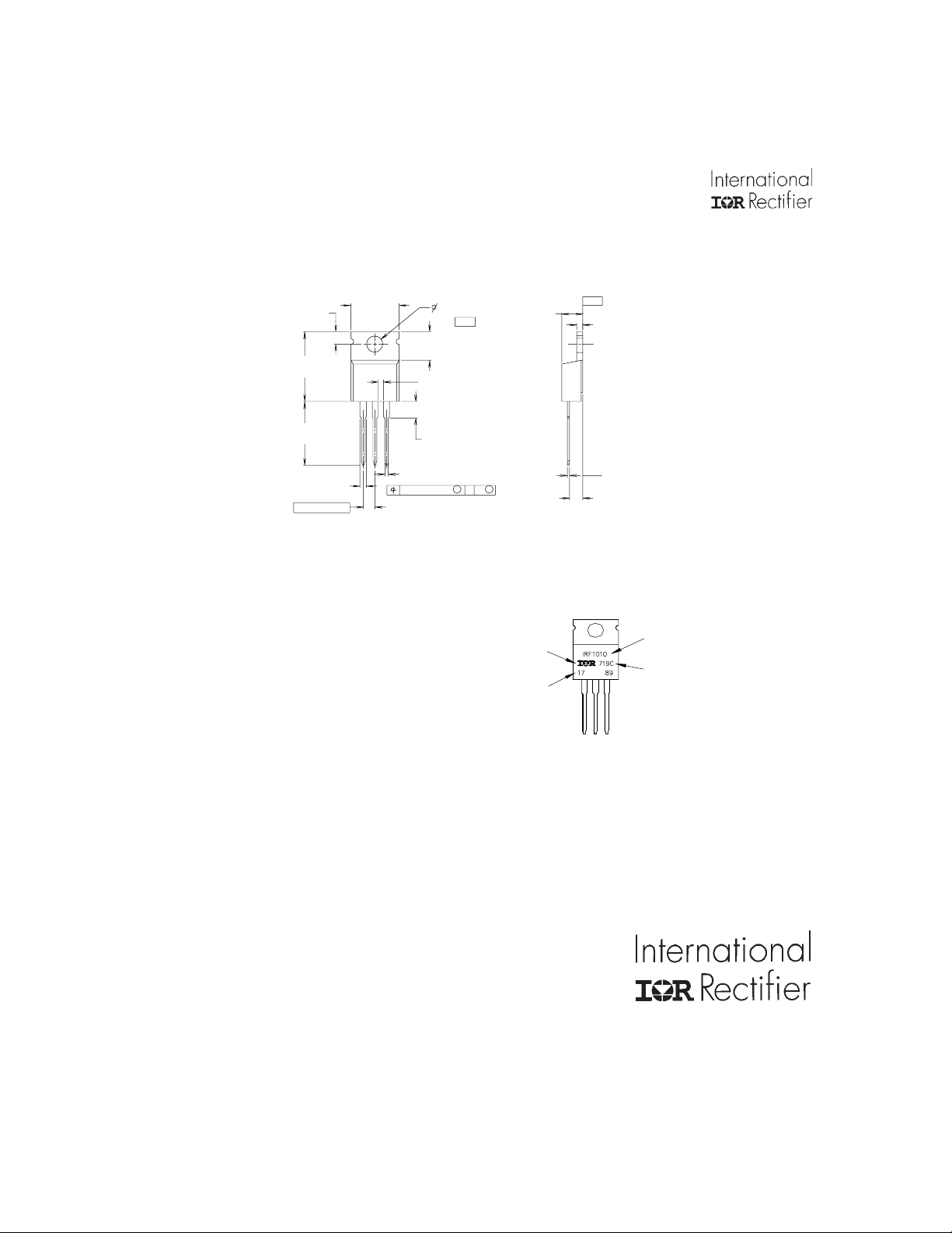
TO-220AB Package Outline
10.54 (.415)
1.40 (.055)
1.15 (.045)
2X
10.29 (.405)
4
1 2 3
2.87 (.113)
2.62 (.103)
15.24 (.600)
14.84 (.584)
14.09 (.555)
13.47 (.530)
3X
2.54 (.100)
NOTES:
1 DIMENSIONING & TOLERANCING PER ANSI Y14.5M, 1982. 3 OUTLINE CONFORMS TO JEDEC OUTLINE TO-220AB.
2 CONTROLLING DIMENSION : INCH 4 HEATSINK & LEAD MEASUREMENTS DO NOT INCLUDE BURRS.
3.78 (.149)
3.54 (.139)
- A -
6.47 (.255)
6.10 (.240)
1.15 (.045)
MIN
4.06 (.160)
3.55 (.140)
0.93 (.037)
3X
0.69 (.027)
0.36 (.014) M B A M
4.69 (.185)
4.20 (.165)
- B -
1.32 (.052)
1.22 (.048)
3X
2.92 (.115)
2.64 (.104)
LEAD ASSIGNMENTS
LEAD ASSIGNMENTS
HEXFET
1 - GATE
2 - DRAIN
1- GATE
3 - SOURCE
2- DRAIN
3- SOUR CE
4 - DRAIN
4- DRAIN
0.55 (.022)
0.46 (.018)
TO-220AB Part Marking Information
EXAMPLE:
TH IS IS AN IRF 1010
LOT CODE 1789
ASS EMBL ED ON WW 19, 1997
IN T HE ASS EMB LY LIN E "C"
Note: "P" in assembly line
position indicates "Lead-Fre e"
INT ERN ATIONAL
RECTIFIER
LOGO
AS SE MBL Y
LOT CODE
IGBTs, CoPACK
1- GATE
2- COLLECTOR
3- EMITTER
4- COLLECTOR
PART NUMBER
DAT E CODE
YEAR 7 = 1997
WEEK 19
LINE C
Notes:
Repetitive rating; pulse width limited by
max. junction temperature.
Starting T
RG = 25Ω, I
I
SD
= 25°C, L = 0.78mH
J
= 34A.
AS
≤ 34, di/dt ≤ 480A/µs, V
DD
≤ V
(BR)DSS
,
Pulse width ≤ 300µs; duty cycle ≤ 2%.
C
eff. is a fixed capacitance that gives the same charging
oss
time as C
oss
while V
is rising from 0 to 80% V
DS
DSS
TJ ≤ 175°C
Data and specifications subject to change without notice.
This product has been designed and qualified for the Industrial market.
Qualification Standards can be found on IR’s Web site.
IR WORLD HEADQUARTERS: 233 Kansas St., El Segundo, California 90245, USA Tel: (310) 252-7105
TAC Fax: (310) 252-7903
Visit us at www.irf.com for sales contact information.7/04
8 www.irf.com
Page 9

Note: For the most current drawings please refer to the IR website at:
http://www.irf.com/package/
 Loading...