

Page 1
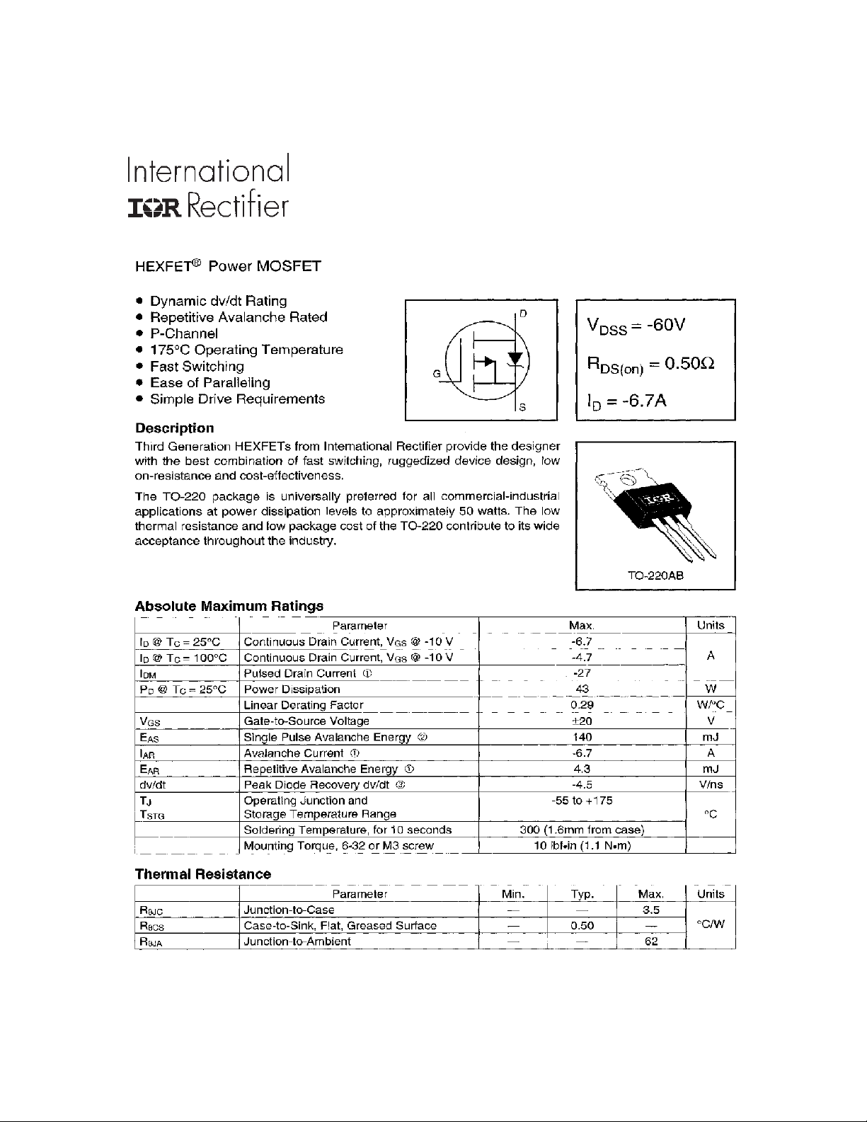
• Lead-Free
Document Number: 91088
www.vishay.com
1
PD - 95628
IRF9Z14PbF
8/3/04
Page 2
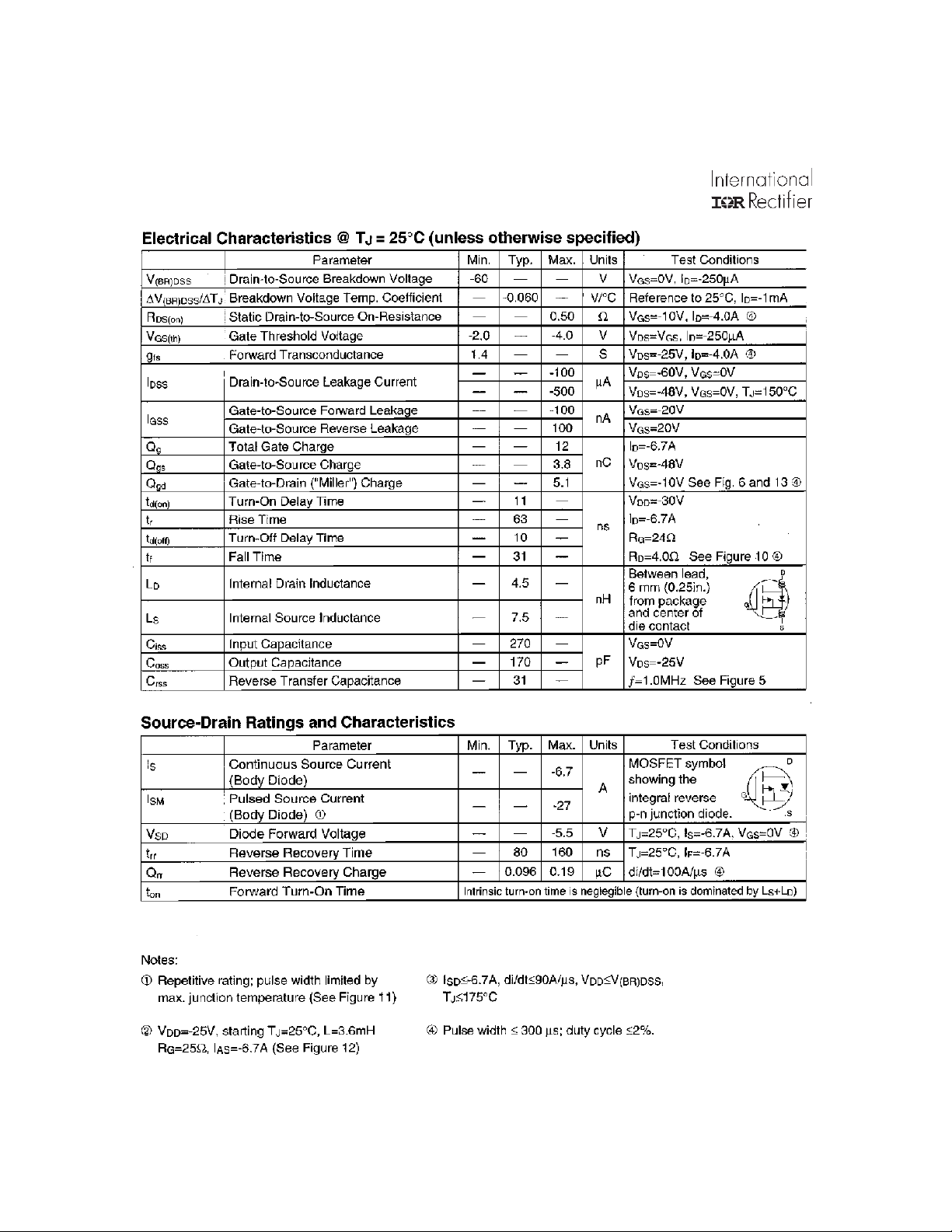
IRF9Z14PbF
Document Number: 91088
www.vishay.com
2
Page 3
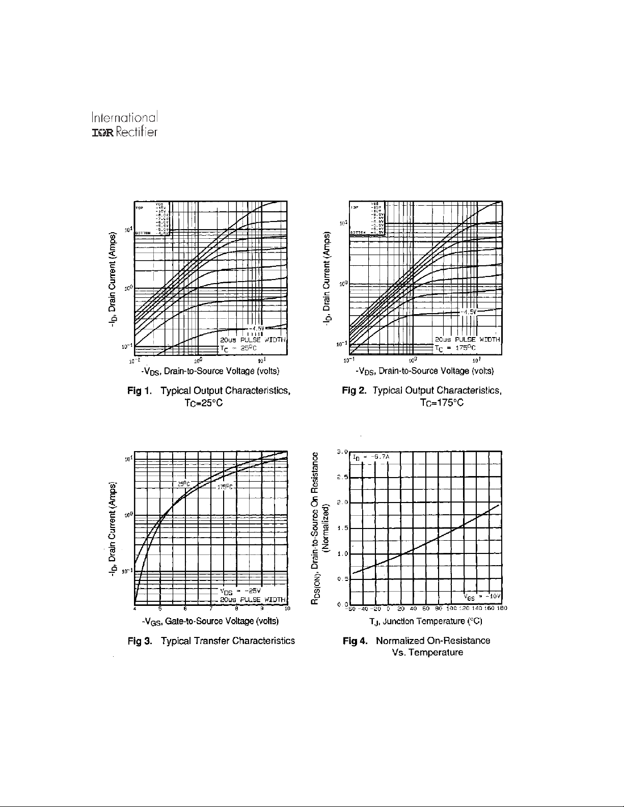
IRF9Z14PbF
Document Number: 91088
www.vishay.com
3
Page 4
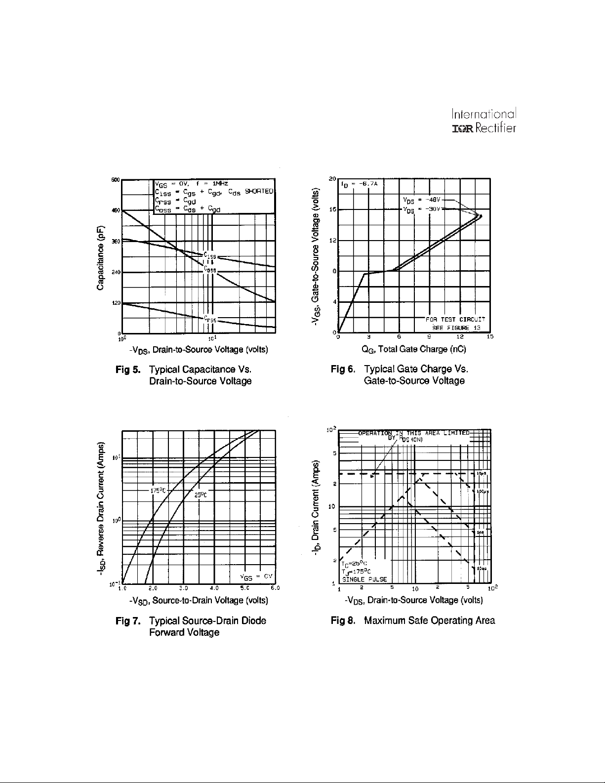
IRF9Z14PbF
Document Number: 91088
www.vishay.com
4
Page 5
IRF9Z14PbF
Document Number: 91088
www.vishay.com
5
Page 6
IRF9Z14PbF
Document Number: 91088
www.vishay.com
6
Page 7
IRF9Z14PbF
Document Number: 91088
www.vishay.com
7
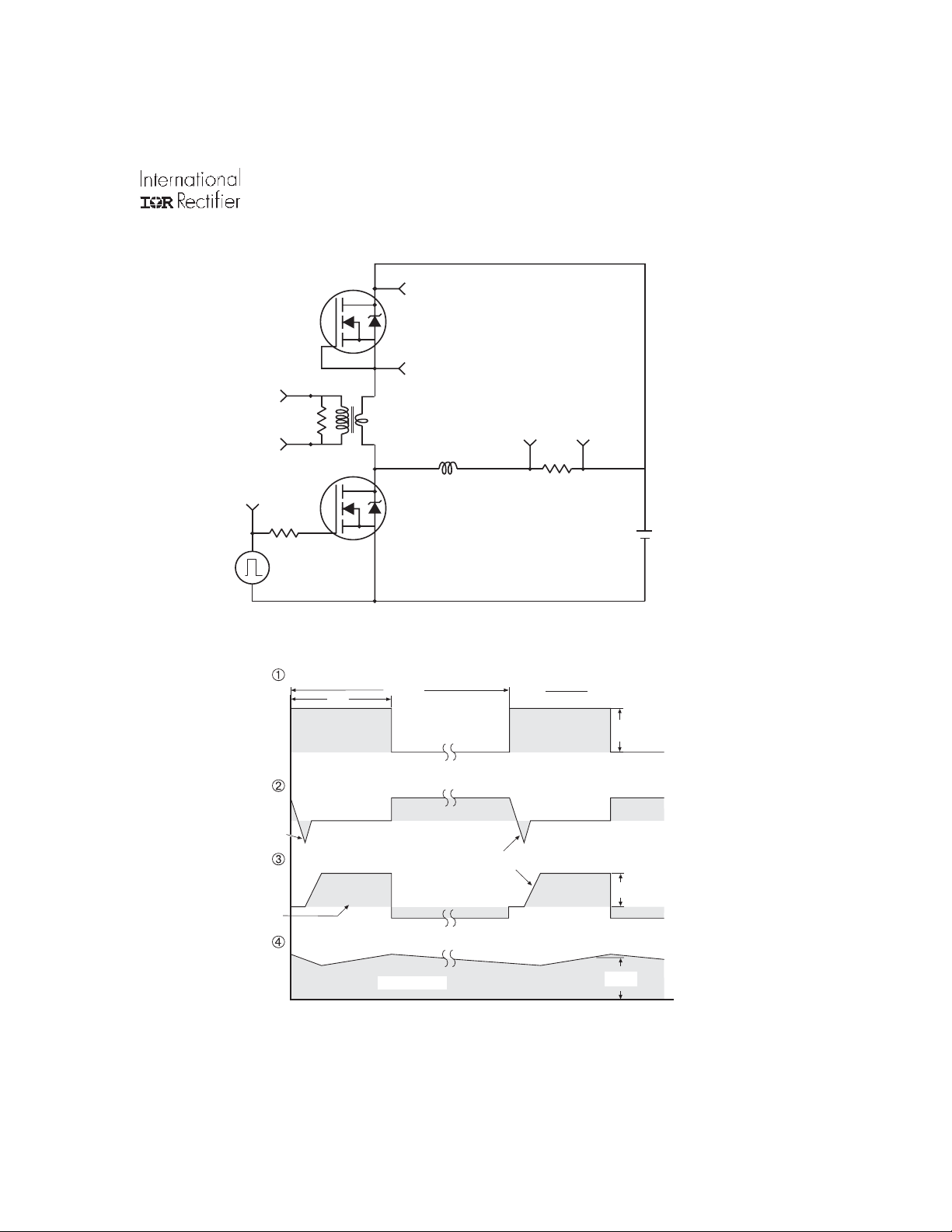
Peak Diode Recovery dv/dt Test Circuit
+
Circuit Layout Considerations
• Low Stray Inductance
• Ground Plane
• Low Leakage Inductance
Current Transformer
-
+
-
-
• dv/dt controlled by R
• ISD controlled by Duty Factor "D"
• D.U.T. - Device Under Test
* Reverse Polarity for P-Channel
** Use P-Channel Driver for P-Channel Measurements
Driver Gate Drive
P.W.
Period
D =
G
+
+
-
P. W .
Period
VGS=10V
Reverse
Recovery
Current
Re-Applied
Voltage
D.U.T. ISDWaveform
Body Diode Forward
Current
D.U.T. VDSWaveform
Body Diode Forward Drop
Inductor Curent
Ripple ≤ 5%
*** V
= 5.0V for Logic Level and 3V Drive Devices
GS
Diode Recovery
di/dt
dv/dt
Fig. 14 For N and P Channel HEXFETS
V
DD
I
SD
Page 8
IRF9Z14PbF
Document Number: 91088
www.vishay.com
8
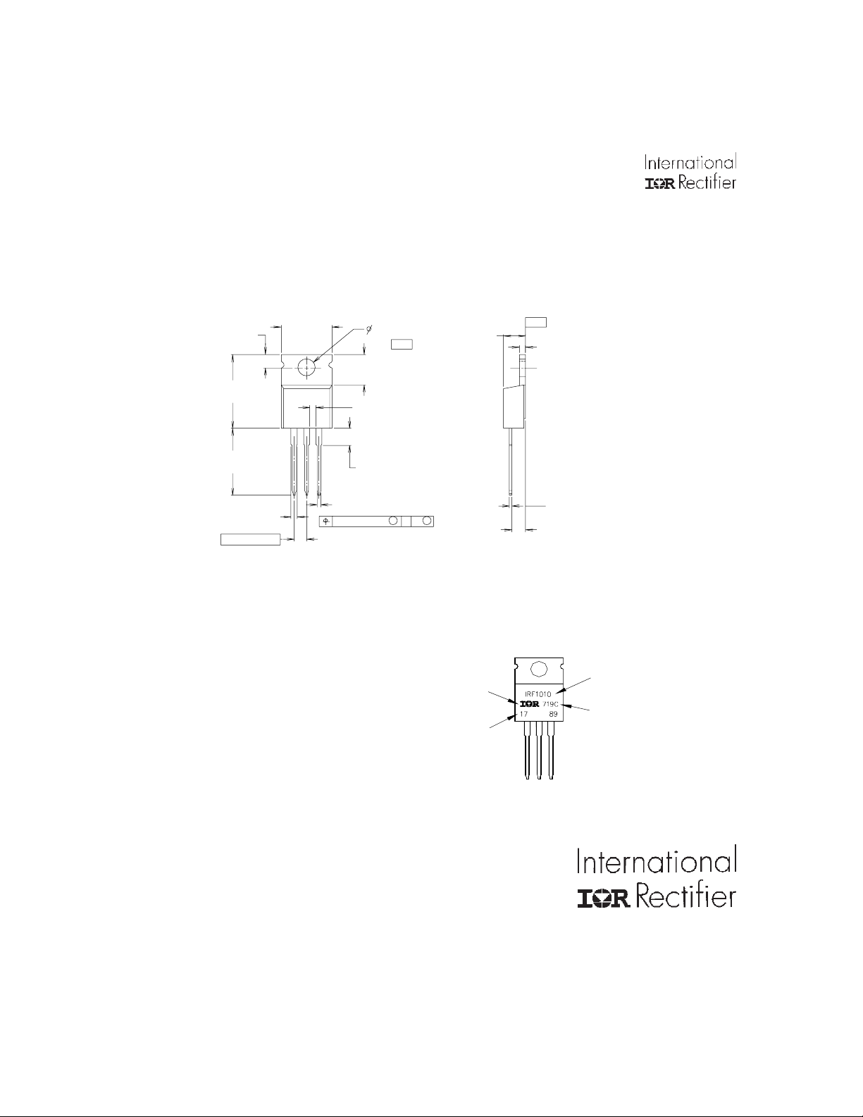
TO-220AB Package Outline
Dimensions are shown in millimeters (inches)
2.87 (. 113)
2.62 (. 103)
15.24 (.600)
14.84 (.584)
14.09 (. 555)
13.47 (. 530)
10.54 (.415)
10.29 (.405)
1 2 3
3.78 (.1 49)
3.54 (.1 39)
- A -
6.47 (.255)
6.10 (.240)
4
1.15 (.0 45)
MIN
4.06 ( .160)
3.55 ( .140)
4.69 (.1 85)
4.20 (.1 65)
- B -
1.32 (.052)
1.22 (.048)
HEXFET
1- GATE
2- DRAIN
3- S OURCE
4- DRAIN
LEAD ASSI GNMENTS
LEAD ASSIGNMENTS
1 - GAT E
2 - DRA IN
3 - SOU RCE
4 - DRA IN
IGBTs, C oPACK
1- GATE
2- COLLECTOR
3- EMITTER
4- COLLECTOR
0.93 (. 037)
3X
1.40 (.055)
3X
1.15 (.045)
2.54 (.1 00)
NOTES:
1 DIMENSION ING & TOLER ANCING PE R ANSI Y 14.5M, 198 2. 3 OUTLINE CONFOR MS TO JEDE C OUTLINE T O-220AB .
2 CONTROL LING DIMEN SION : INCH 4 HEA TSINK & LE AD MEAS UREMENT S DO NOT INCLUDE BURRS.
2X
0.69 (. 027)
0.36 (.014) M B A M
0.55 (. 022)
3X
0.46 (. 018)
2.92 (. 115)
2.64 (. 104)
TO-220AB Part Marking Information
EXAMPLE:
T HIS IS AN IRF 1010
LOT CODE 1789
ASS EMBL ED ON WW 19, 1997
IN THE ASSEMBLY LINE "C"
Note: "P" in assembly line
position indicates "Lead-Free"
INT ER NAT IONAL
RECTIF IER
LOGO
ASSEMBLY
LOT CODE
Data and specifications subject to change without notice.
PART NU MB ER
DATE CODE
YEAR 7 = 1997
WEEK 19
LINE C
IR WORLD HEADQUARTERS: 233 Kansas St., El Segundo, California 90245, USA Tel: (310) 252-7105
TAC Fax: (310) 252-7903
08/04
Page 9

Legal Disclaimer Notice
Vishay
Notice
The products described herein were acquired by Vishay Intertechnology, Inc., as part of its acquisition of
International Rectifier’s Power Control Systems (PCS) business, which closed in April 2007. Specifications of the
products displayed herein are pending review by Vishay and are subject to the terms and conditions shown below.
Specifications of the products displayed herein are subject to change without notice. Vishay Intertechnology, Inc., or
anyone on its behalf, assumes no responsibility or liability for any errors or inaccuracies.
Information contained herein is intended to provide a product description only. No license, express or implied, by
estoppel or otherwise, to any intellectual property rights is granted by this document. Except as provided in Vishay's
terms and conditions of sale for such products, Vishay assumes no liability whatsoever, and disclaims any express
or implied warranty, relating to sale and/or use of Vishay products including liability or warranties relating to fitness
for a particular purpose, merchantability, or infringement of any patent, copyright, or other intellectual property right.
The products shown herein are not designed for use in medical, life-saving, or life-sustaining applications.
Customers using or selling these products for use in such applications do so at their own risk and agree to fully
indemnify Vishay for any damages resulting from such improper use or sale.
International Rectifier
are registered trademarks of International Rectifier Corporation in the U.S. and other countries. All other product
names noted herein may be trademarks of their respective owners.
®
, IR®, the IR logo, HEXFET®, HEXSense®, HEXDIP®, DOL®, INTERO®, and POWIRTRAIN
®
Document Number: 99901 www.vishay.com
Revision: 12-Mar-07 1
 Loading...