

Page 1
PD - 9.1099B
2
PRELIMINARY
HEXFET® Power MOSFET
Advanced Process Technology
Ultra Low On-Resistance
Dual N and P Channel Mosfet
Surface Mount
Available in Tape & Reel
Dynamic dv/dt Rating
Fast Switching
Description
Fourth Generation HEXFETs from International Rectifier utilize advanced
processing techniques to achieve the lowest possible on-resistance per silicon
area. This benefit, combined with the fast switching speed and ruggedized device
design for which HEXFET Power MOSFETs are well known, provides the designer
with an extremely efficient device for use in a wide variety of applications.
The SO-8 has been modified through a customized leadframe for enhanced
thermal characteristics and multiple-die capability making it ideal in a variety of
power applications. With these improvements, multiple devices can be used in an
application with dramatically reduced board space. The package is designed for
vapor phase, infra-red, or wave soldering techniques. Power dissipation of greater
than 0.8W is possible in a typical PCB mount application.
S1
G1
S2
G2
N-CHANNEL MOSFET
1
2
3
4
P-CHA NNEL MOSFET
Top View
8
D1
7
D1
6
D
5
D2
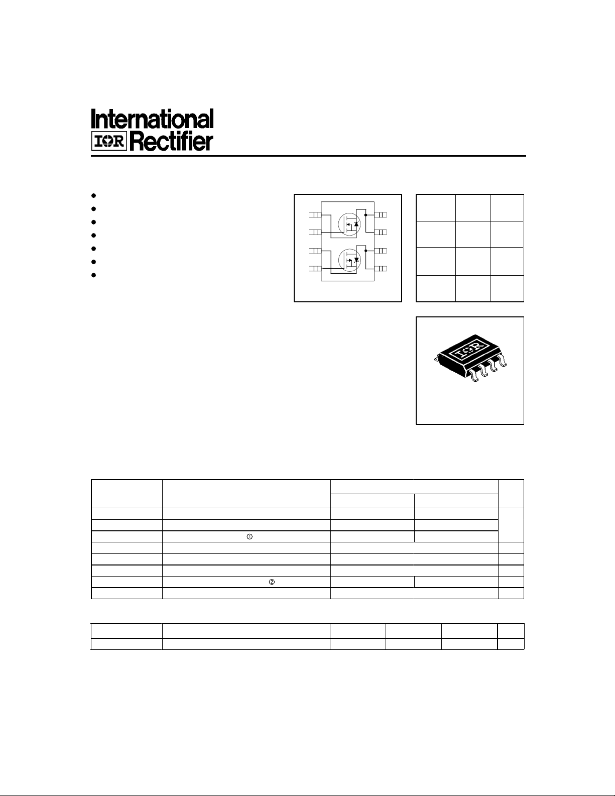
IRF7107
N-Ch P-Ch
V
R
DS(on)
DSS
I
20V -20V
0.125Ω 0.160Ω
3.0A -2.8A
D
SO-8
Absolute Maximum Ratings
Max.
N-Channel P-Channel
ID @ TC = 25°C Continuous Drain Current, VGS @ 10V 3.0 -2.8
ID @ TC = 70°C Continuous Drain Current, VGS @ 10V 2.5 -2.3 A
I
DM
PD @TC = 25°C Power Dissipation 2.0
V
GS
dv/dt Peak Diode Recovery dv/dt 3.0 -1.3 V/ns
T
J, TSTG
Pulsed Drain Current 10 -10
Linear Derating Factor 0.016
Gate-to-Source Voltage ± 20 V
Junction and Storage Temperature Range -55 to + 150 °C
Thermal Resistance
Parameter Min. Typ. Max. Units
R
θJA
** When mounted on 1" square PCB (FR-4 or G-10 Material).
For recommended footprint and soldering techniques refer to application note #AN-994.
Junction-to-Ambient (PCB Mount)** –––– –––– 62.5
Revision 3
77
Page 2
IRF7107
Electrical Characteristics @ TJ = 25°C (unless otherwise specified)
V
(BR)DSS
∆V
(BR)DSS
R
DS(ON)
V
GS(th)
g
fs
I
DSS
I
GSS
Q
g
Q
gs
Q
gd
t
d(on)
t
r
t
d(off)
t
f
L
D
L
S
C
iss
C
oss
C
rss
Drain-to-Source Breakdown Voltage
/∆TJBreakdown Voltage Temp. Coefficient
Static Drain-to-Source On-Resistance
Gate Threshold Voltage
Forward Transconductance
Drain-to-Source Leakage Current
Gate-to-Source Forward Leakage N-P –– — ±100 nA VGS = ± 20V
Total Gate Charge
Gate-to-Source Charge
Gate-to-Drain ("Miller") Charge
Turn-On Delay Time
Rise Time
Turn-Off Delay Time
Fall Time
Internal Drain Inductace N-P — 4.0 — Between lead tip
Internal Source Inductance N-P — 6.0 — and center of die contact
Input Capacitance
Output Capacitance
Reverse Transfer Capacitance
Parameter Min. Typ. Max. Units Conditions
N-Ch 20 — — VGS = 0V, ID = 250µA
P-Ch -20 — — VGS = 0V, ID = -250µA
N-Ch — 0.037 — Reference to 25°C, ID = 1mA
P-Ch — 0.015 — Reference to 25°C, ID = -1mA
— — 0.125 VGS = 10V, ID = 3.0A
N-Ch
— — 0.250 VGS = 4.5V, ID = 1.50A
— — 0.160 VGS = -10V, ID = -3.0A
P-Ch
— — 0.300 VGS = -4.5V, ID = -1.5A
N-Ch 1.0 — — VDS = VGS, ID = 250µA
P-Ch -1.0 — — VDS = VGS, ID = -250µA
N-Ch — 4.4 — VDS = 15V, ID = 3.0A
P-Ch — 3.3 — VDS = -15V, ID = -3A
V
V/°C
Ω
V
S
N-Ch — — 2.0 VDS = 16V, VGS = 0V
P-Ch — — -2.0 VDS = -16V, VGS = 0V
N-Ch — — 25 VDS = 16V, VGS = 0V, TJ =125°C
µA
P-Ch — — -25 VDS = -16V, VGS = 0V, TJ = 125°C
N-Ch — 9.1 25
P-Ch — 11 25
N-Ch — 1.2 —
P-Ch — 1.8 —
N-Ch — 2.5 —
P-Ch — 3.5 —
N-Ch — 5.0 15
P-Ch — 12 40
N-Ch — 10 20
P-Ch — 19 40
N-Ch — 29 50
P-Ch — 42 90
N-Ch — 22 50
P-Ch — 42 63
N-Channel
ID = 2.3A, VDS = 10V, VGS = 10V
nC
P-Channel
ID = -2.3A, VDS = -10V, VGS = -10V
N-Channel
VDD = 20V, ID = 1.0A, RG = 6.0Ω,
RD = 20Ω
ns
P-Channel
VDD = -20V, ID = -1.0A, RG = 6.0Ω,
RD = 20Ω
nH
N-Ch — 300 —
P-Ch — 320 —
N-Ch — 260 —
P-Ch — 300 —
N-Ch — 62 —
P-Ch — 95 —
N-Channel
VGS = 0V, VDS = 15V, ƒ = 1.0MHz
pF
P-Channel
VGS = 0V, VDS = -15V, ƒ = 1.0MHz
Source-Drain Ratings and Characteristics
Parameter Min. Typ. Max. Units Conditions
I
S
I
SM
V
SD
t
rr
Q
rr
t
on
Continuous Source Current (Body Diode)
Pulsed Source Current (Body Diode)
Diode Forward Voltage
Reverse Recovery Time
Reverse Recovery Charge
Forward Turn-On Time N-P
Notes:
Repetitive rating; pulse width limited by
max. junction temperature. ( See fig. 11 )
N-Ch — — 1.7
P-Ch — — -1.6
N-Ch — — 10
P-Ch — — -10
N-Ch — 0.90 1.2 TJ = 25°C, IS = 1.7A, VGS = 0V
P-Ch — -1.4 -1.6 TJ = 25°C, IS = -1.3A, VGS = 0V
N-Ch — 69 100
P-Ch — 69 100
N-Ch — 58 120
P-Ch — 64 96
N-Channel I
P-Channel I
Pulse width ≤ 300µs; duty cycle ≤ 2%.
A
V
N-Channel
ns
TJ = 25°C, IF = 1.25A, di/dt = 100A/µs
P-Channel
nC
TJ = 25°C, IF = -1.25A, di/dt = 100A/µs
Intrinsic turn-on time is neglegible (turn-on is dominated by LS+LD)
≤ 2.3A, di/dt ≤ 100A/µs, V
SD
≤ -1.25A, di/dt ≤ 50A/µs, V
SD
DD
DD
≤ V
≤ V
(BR)DSS
(BR)DSS
, TJ ≤ 150°C
, TJ ≤ 150°C
78
Page 3
100
A
A
A
A
A
A
10
VGS
TOP 15V
10V
8.0 V
7.0 V
6.0 V
5.5 V
5.0 V
BOTTOM 4.5V
4.5V
100
10
VGS
TOP 15 V
10V
8.0V
7.0V
6.0V
5.5V
5.0V
BOTTOM 4.5 V
IRF7107
4.5V
1
D
I , Drain-to-Source Current (A)
0.1
0.01 0.1 1 10 100
V , Drain-to-Source Voltage (V)
DS
20µs PULSE WIDTH
T = 25°C
J
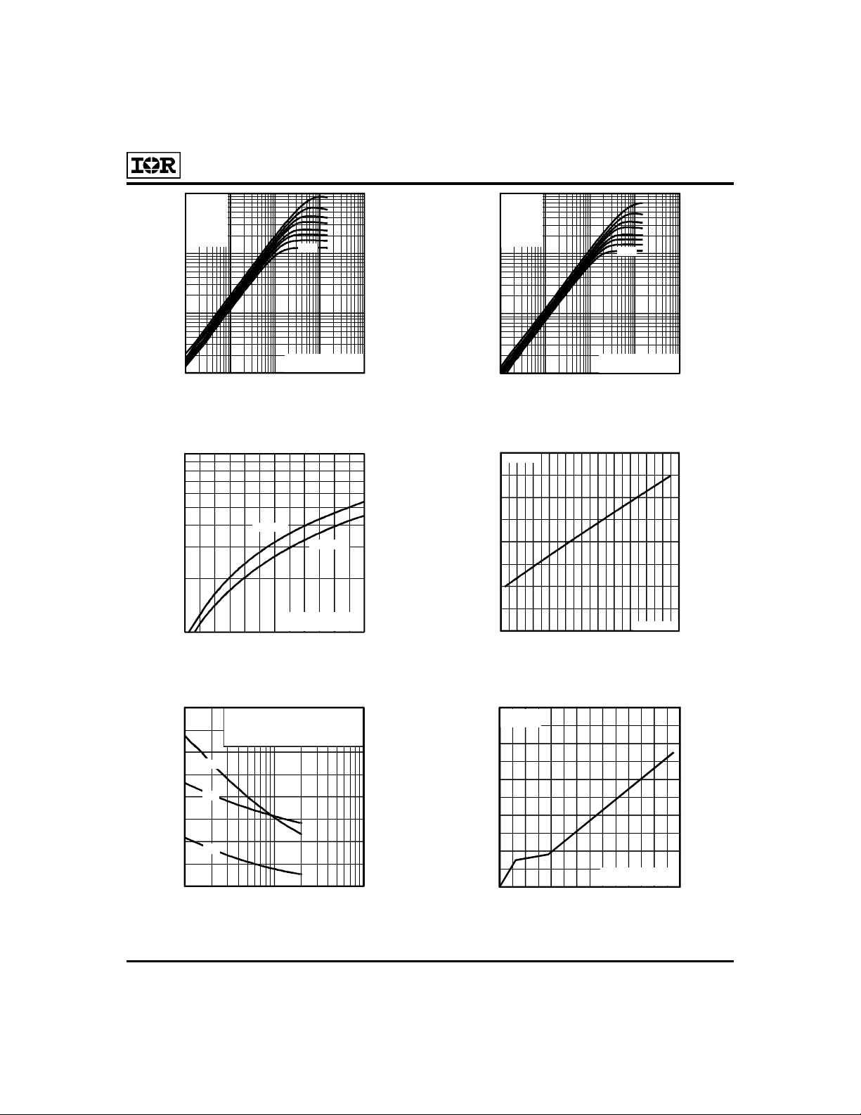
Fig 1. Typical Output Characteristics,
TJ = 25oC
100
T = 25°C
J
T = 150°C
J
D
I , Drain-to-Source Current (A)
10
4 5 6 7 8 9 10
V , Gate-to-Source Voltage (V)
GS
V = 15V
DS
20µs PULSE WIDTH
Fig 3. Typical Transfer Characteristics
800
600
400
C, Capacitance (pF)
200
0
V = 0V, f = 1MHz
GS
C = C + C , C SHORTED
iss gs gd ds
C = C
rss gd
C = C + C
oss ds gd
C
oss
C
iss
C
rss
1 10 100
V , Drain-to-Source Voltage (V)
DS
Fig 5. Typical Capacitance Vs.
Drain-to-Source Voltage
1
D
I , Drain-to-Source Current (A)
0.1
0.01 0.1 1 10 100
V , Drain-to-Source Voltage (V)
DS
20µs PULSE WIDTH
T = 150°C
J
Fig 2. Typical Output Characteristics,
TJ = 150oC
2.0
I = 3.0A
D
1.5
1.0
(Normalized)
0.5
DS(on)
R , Drain-to-Source On Resistance
0.0
-60 -40 -20 0 20 40 60 80 100 120 140 160
T , Junction Temperature (°C)
J
V = 10V
GS
Fig 4. Normalized On-Resistance
Vs. Temperature
20
I = 2.3A
D
V = 10V
DS
16
12
8
4
GS
V , Gate-to-Source Voltage (V)
0
0 2 4 6 8 10 12 14
Q , Total Gate Charge (nC)
G
FOR TEST CIRCUIT
SEE FIGURE 11
Fig 6. Typical Gate Charge Vs.
Gate-to-Source Voltage
79
Page 4
IRF7107
A
A
A
100
100
OPERATION IN THIS AREA LIMITED
BY R
DS(on)
10
1
SD
I , Reverse Drain Current (A)
0.1
0.4 0.6 0.8 1.0 1.2 1.4
T = 150°C
J
T = 25°C
J
V = 0V
GS
V , Source-to-Drain Voltage (V)
SD
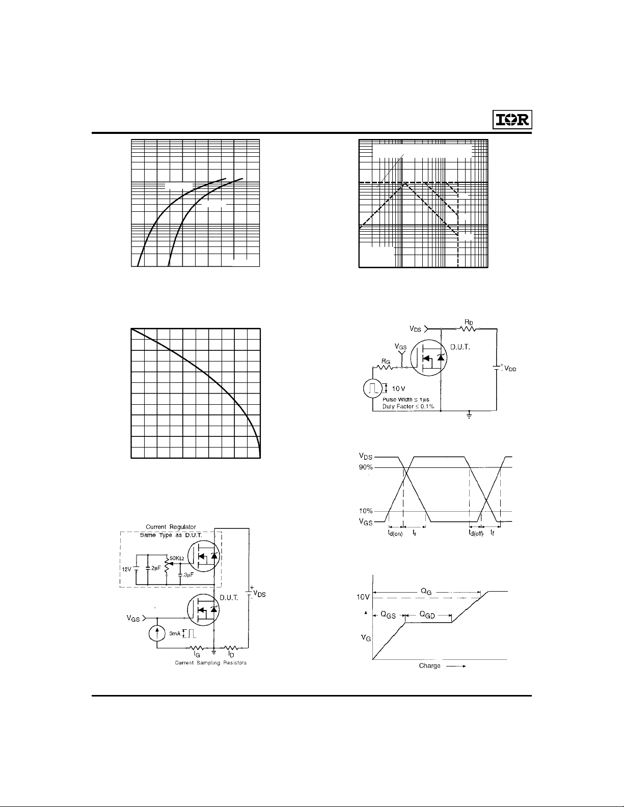
Fig 7. Typical Source-Drain Diode
Forward Voltage
3.0
2.5
2.0
1.5
1.0
D
I , Drain Current (Amps)
0.5
0.0
25 50 75 100 125 150
T , Ambient Temperature (°C)
A
Fig 9. Maximum Drain Current Vs.
Ambient Temperature
10
1ms
1
D
I , Drain Current (A)
T = 25°C
A
T = 150°C
J
Single Pulse
0.1
0.1 1 10 100
V , Drain-to-Source Voltage (V)
DS
10ms
100ms
Fig 8. Maximum Safe Operating Area
Fig 10a. Switching Time Test Circuit
Fig 10b. Switching Time Waveforms
Fig 11b. Basic Gate Charge WaveformFig 11a. Gate Charge Test Circuit
80
Page 5
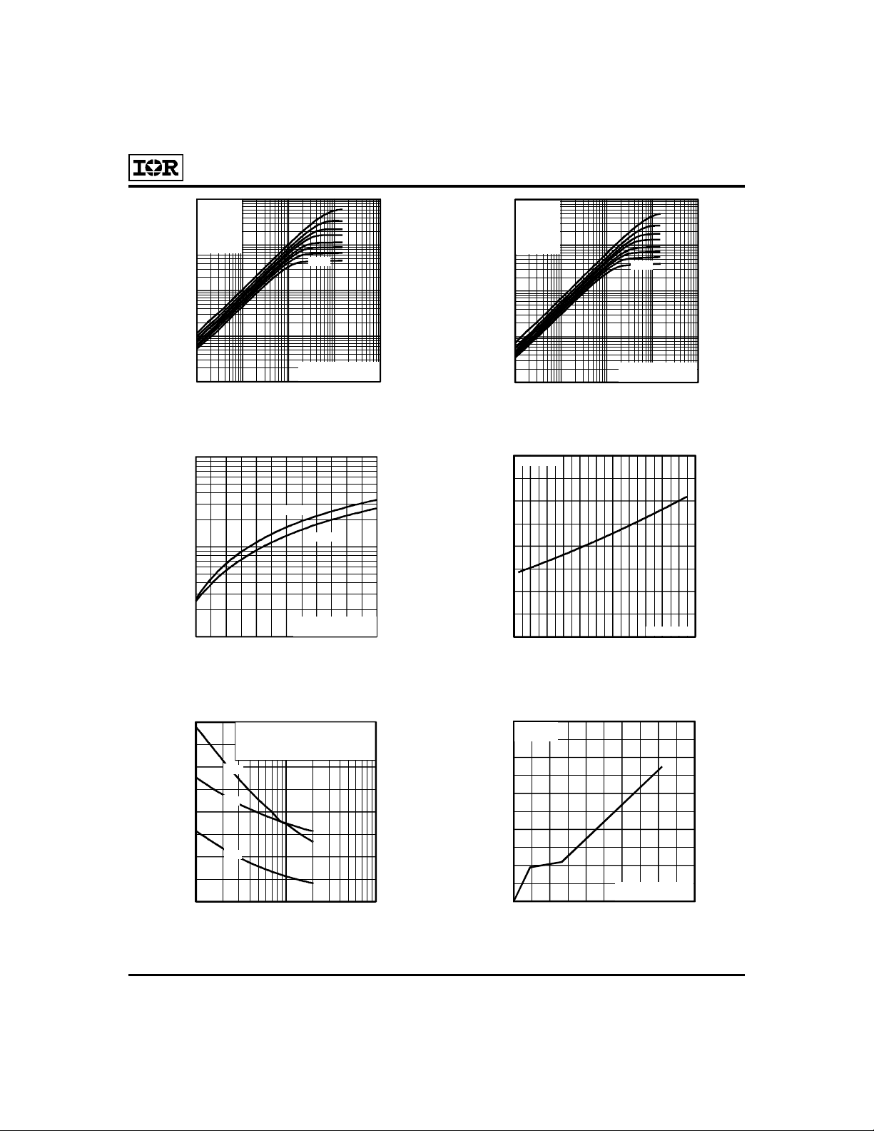
IRF7107
A
A
A
A
A
A
100
VGS
TOP - 15V
- 10 V
- 8.0V
- 7.0V
- 6.0V
- 5.5V
- 5.0V
10
BOT T OM - 4.5V
-4.5V
1
0.1
D
-I , Drain-to-Source Current (A)
0.01
0.01 0.1 1 10 100
-V , Drain-to-Source Voltage (V)
DS
20µs PULSE WIDTH
T = 25°C
J
Fig 12. Typical Output Characteristics,
TJ = 25oC
100
T = 25°C
J
T = 150°C
10
D
-I , Drain-to-Source Current (A)
1
4 5 6 7 8 9 10
-V , Gate-to-Source Voltage (V)
GS
J
V = -15V
DS
20µs PULSE WID TH
Fig 14. Typical Transfer Characteristics
800
600
400
C, Capacitance (pF)
200
0
1 10 100
V = 0V, f = 1MHz
GS
C = C + C , C SHORTED
iss gs gd ds
C = C
rss gd
C = C + C
oss ds gd
C
oss
C
iss
C
rss
-V , Drain-to-Source Voltage (V)
DS
Fig 16. Typical Capacitance Vs.
Drain-to-Source Voltage
100
VGS
TOP - 15 V
- 10V
- 8.0V
- 7.0V
- 6.0V
- 5.5V
- 5.0V
10
BOTTOM - 4.5V
-4.5V
1
0.1
D
-I , Drain-to-Source Current (A)
0.01
0.01 0.1 1 10 100
-V , Drain-to-Source Voltage (V)
Fig 13. Typical Output Characteristics,
DS
20µs PULSE WIDTH
T = 150°C
J
TJ = 150oC
2.0
I = -2.8A
D
1.5
1.0
(Normalized)
0.5
DS(on)
R , Drain-to-Source On Resistance
0.0
-60 -40 -20 0 20 40 60 80 100 120 140 160
T , Junction Temperature (°C)
J
V = -10V
GS
Fig 15. Normalized On-Resistance
Vs. Temperature
20
I = -2.3A
D
V = -10V
DS
16
12
8
4
GS
-V , Gate-to-Source Voltage (V)
0
0 4 8 12 16 20
Q , Total G ate Charge (nC)
G
FOR TEST CIRCUIT
SEE FIGURE 22
Fig 17. Typical Gate Charge Vs.
Gate-to-Source Voltage
81
Page 6
IRF7107
A
A
A
100
100
OPERATION IN THIS AREA LIMITED
BY R
DS(on)
10
1
SD
-I , Reverse Drain Current (A)
0.1
0.4 0.8 1.2 1.6 2.0
-V , Source-to-Drain Voltage (V)
T = 150°C
J
T = 25°C
J
V = 0V
GS
SD
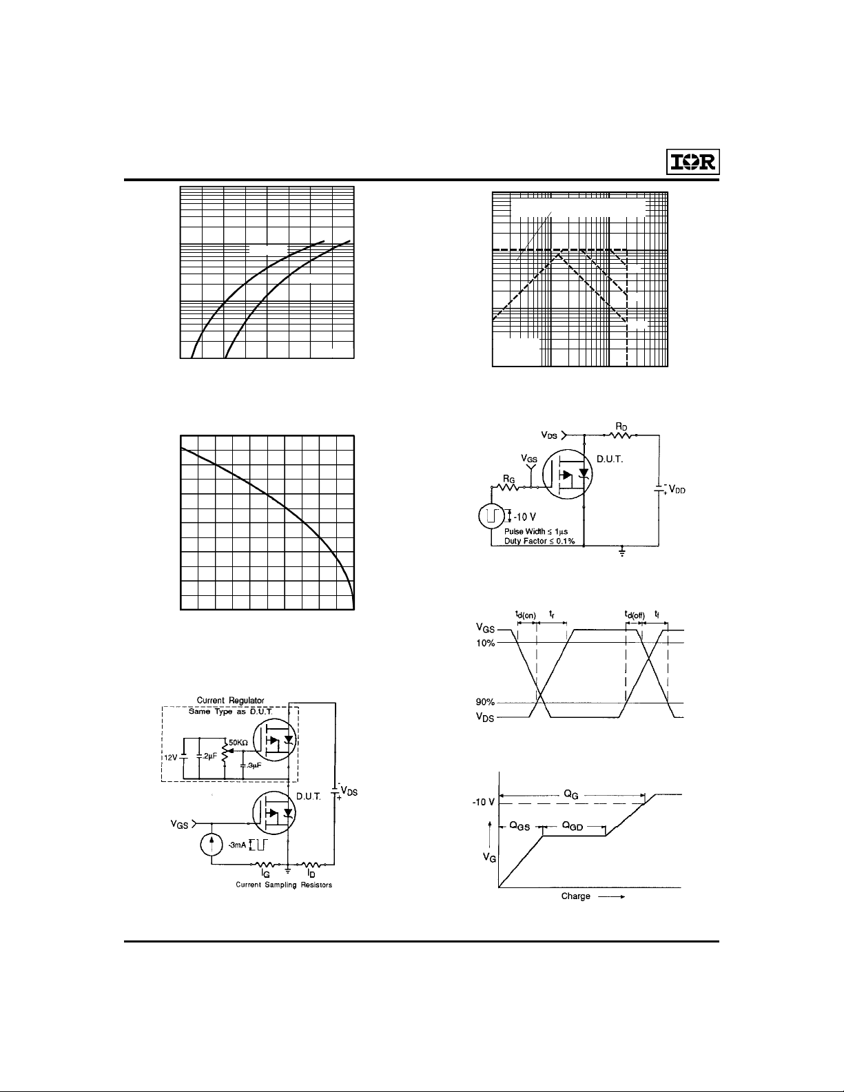
Fig 18. Typical Source-Drain Diode
Forward Voltage
3.0
2.5
2.0
1.5
1.0
D
-I , Drain Current (Amps)
0.5
0.0
25 50 75 100 125 150
T , A mbient Temperature (°C)
A
Fig 20. Maximum Drain Current Vs.
Ambient Temperature
10
1ms
1
D
-I , Drain Current (A)
T = 25°C
A
T = 150°C
J
Single Pulse
0.1
0.1 1 10 100
-V , Drain-to-Source Voltage (V)
DS
10ms
100ms
Fig 19. Maximum Safe Operating Area
Fig 21a. Switching Time Test Circuit
Fig 21b. Switching Time Waveforms
Fig 22a. Gate Charge Test Circuit
Fig 22b. Basic Gate Charge Waveform
82
Page 7
100
IRF7107
D = 0.50
thJA
Thermal Response (Z )
0.20
10
0.10
0.05
P
0.02
1
0.01
SINGLE PULSE
(THERMAL RE SPONSE)
0.1
0.00001 0.0001 0.001 0.01 0.1 1 10 100 1000
t , Rectangular Pulse Duration (sec)
1
N otes:
1. Duty factor D = t / t
2. Peak T = P x Z + T
DM
J
DM
t
1
t
2
2
1
th JA
A
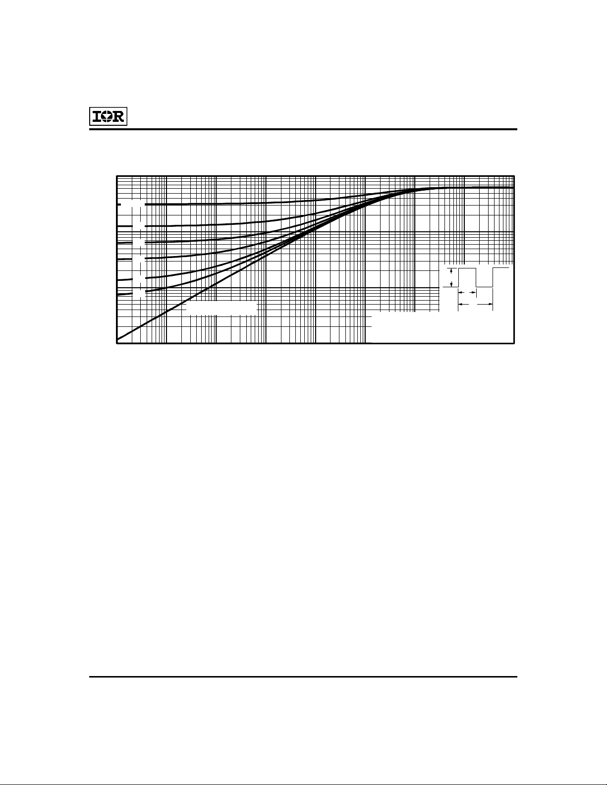
Fig 23. Maximum Effective Transient Thermal Impedance, Junction-to-Ambient
Refer to the Appendix Section for the following:
A
Appendix A: Figure 24, Peak Diode Recovery dv/dt Test Circuit — See page 329.
Appendix B: Package Outline Mechanical Drawing — See page 332.
Appendix C: Part Marking Information — See page 332.
Appendix D: Tape and Reel Information — See page 336.
83
 Loading...