

Page 1
PROVISIONAL
PD - 94364A
IRF6603
l Application Specific MOSFETs
l Ideal for CPU Core DC-DC Converters
l Low Conduction Losses
l High Cdv/dt Immunity
l Low Profile (<0.7 mm)
l Dual Sided Cooling Compatible
l Compatible with existing Surface Mount
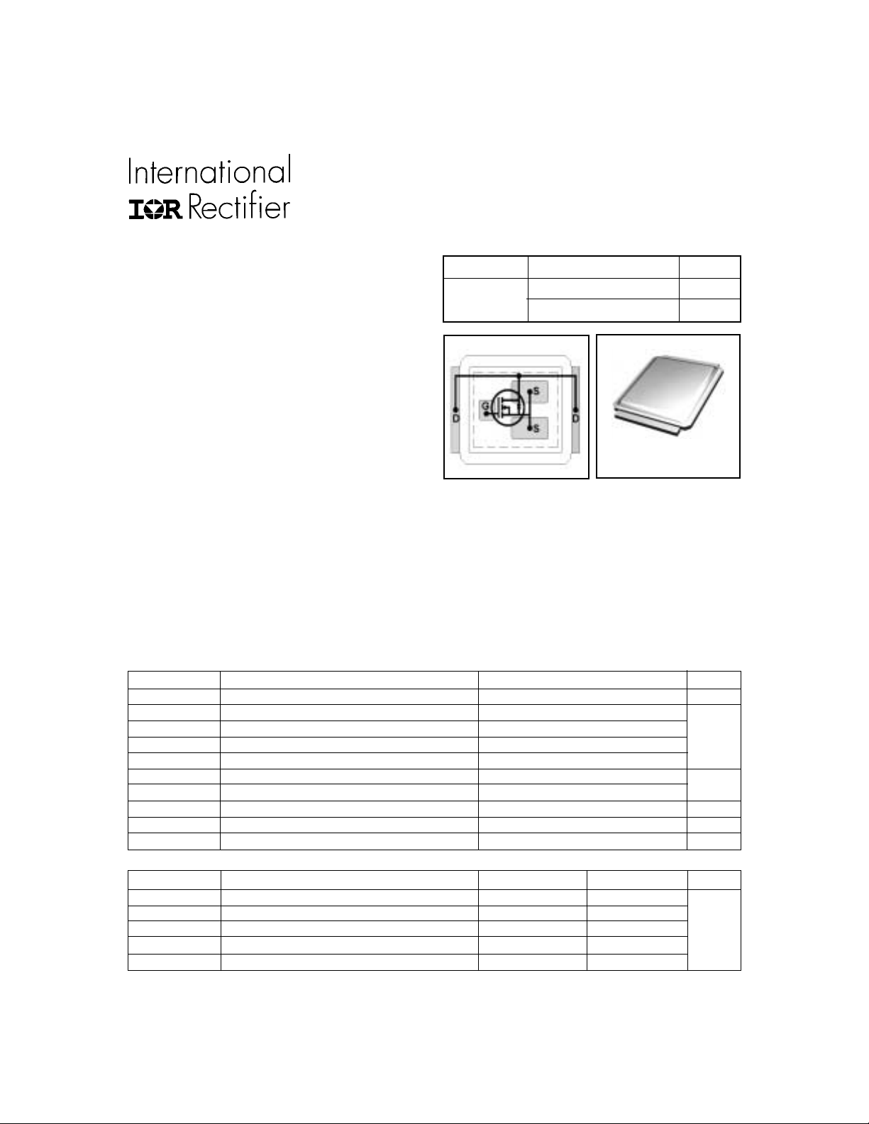
DirectFET
V
DSS
30V 3.9mΩ@VGS = 10V 28A
5.5mΩ@VGS = 4.5V 22A
R
DS(on)
TM
Power MOSFET
max I
D
Techniques
DirectFET™ ISOMETRIC
Description
The IRF6603 combines the latest HEXFET® Power MOSFET Silicon technology with the advanced DirectFETTM packaging
to achieve the lowest on-state resistance in a package that has the footprint of an SO-8 and only 0.7 mm profile. The DirectFET
package is compatible with existing layout geometries used in power applications, PCB assembly equipment and vapor
phase, infra-red or convection soldering techniques. The DirectFET package allows dual sided cooling to maximize thermal
transfer in power systems, IMPROVING previous best thermal resistance by 80%.
The IRF6603 balances both low resistance and low charge along with ultra low package inductance to reduce both conduction
and switching losses. The reduced total losses make this product ideal for high efficiency DC-DC converters that power the
latest generation of processors operating at higher frequencies. The IRF6603 has been optimized for parameters that are
critical in synchronous buck converters including Rds(on), gate charge and Cdv/dt-induced turn on immunity. The IRF6603
offers particularly low Rds(on) and high Cdv/dt immunity for synchronous FET applications.
Absolute Maximum Ratings
Parameter Max. Units
V
DS
ID @ TC = 25°C Continuous Drain Current, VGS @ 10V 84
ID @ TA = 25°C Continuous Drain Current, VGS @ 10V 28
ID @ TA = 70°C Continuous Drain Current, VGS @ 10V 22 A
I
DM
PD @TA = 25°C Power Dissipation 5.0
PD @TA = 70°C Power Dissipation 3.2
V
GS
T
J, TSTG
Drain- Source Voltage 30 V
Pulsed Drain Current 220
W
Linear Derating Factor 40 mW/°C
Gate-to-Source Voltage +20/-12 V
Junction and Storage Temperature Range -55 to + 150 °C
Thermal Resistance
Symbol Parameter Typ. Max. Units
R
θJA
R
θJA
R
θJA
R
θJC
R
θJ-PCB
Junction-to-Ambient ––– 25
Junction-to-Ambient ––– 12.5
Junction-to-Ambient ––– 25 °C/W
Junction-to-Case ––– 3.0
Junction-to-PCB mounted ––– 1.0
www.irf.com 1
01/24/02
Page 2
IRF6603
PROVISIONAL
Static @ TJ = 25°C (unless otherwise specified)
Parameter Min. Typ. Max. Units Conditions
V
(BR)DSS
∆V
(BR)DSS
R
DS(on)
V
GS(th)
I
DSS
I
GSS
Drain-to-Source Breakdown Voltage 30 ––– ––– VVGS = 0V, ID = 250µA
/∆T
Breakdown Voltage Temp. Coefficient
J
Static Drain-to-Source On-Resistance
––– 0.02 ––– V/°C Reference to 25°C, ID = 1mA
––– 2.8 3.9 VGS = 10V, ID = 28A
––– 3.9 5.5 VGS = 4.5V, ID = 22A
mΩ
Gate Threshold Voltage 1.0 2. 5 3.2 V VDS = VGS, ID = 250µA
Drain-to-Source Leakage Current
––– ––– 30
––– ––– TBA VDS = 24V, VGS = 0V, TJ = 125°C
Gate-to-Source Forward Leakage ––– ––– 100 VGS = 20 V
Gate-to-Source Reverse Leakage ––– ––– -100
µA
nA
= 24V, VGS = 0V
V
DS
VGS = -12 V
Dynamic @ TJ = 25°C (unless otherwise specified)
Symbol Parameter Min. Typ. Max. Units Conditions
g
fs
Q
Q
Q
Q
Q
Q
R
t
d(on)
t
r
t
d(off)
t
f
C
C
C
g
g
gs1
gs2
gd
oss
g
iss
oss
rss
Forward Transconductance TBA ––– ––– SVDS = 16V, ID = 28A
Total Gate Charge Cont FET ––– 86 120 VGS = 10V, VDS = 16V, ID = 28A
Total Gate Charge Sync FET ––– 69 ––– VGS = 10V, VDS < 100mV
Pre-Vth Gate-Source Charge ––– 12 ––– VDS = 16V, ID = 28A
Post-Vth Gate-Source Charge ––– 2.5 ––– nC
Gate to Drain Charge ––– 19 28
Output Charge ––– 32 ––– VDS = 16V, VGS = 0V
Gate Resistance ––– 2.0 2.5 Ω
Turn-On Delay Time ––– TBA ––– VDD = 16V
Rise Time ––– TBA ––– ns ID = 28A
Turn-Off Delay Time ––– TBA ––– VGS = 5.0V
Fall Time ––– TBA ––– Clamped Inductive Load
Input Capacitance ––– TBA ––– VGS = 0V
Output Capacitance ––– TBA ––– pF VDS = 16V
Reverse Transfer Capacitance ––– TBA ––– ƒ = 1.0MHz
Avalanche Characteristics
Symbol Parameter Typ. Max. Units
E
AS
I
AR
Single Pulse Avalanche Energy ––– 553 mJ
Avalanche Current ––– TBA A
Diode Characteristics
Symbol Parameter Min. Typ. Max. Units Conditions
I
S
I
SM
V
SD
t
rr
Q
rr
Q
rr(s)
Continuous Source Current MOSFET symbol
(Body Diode)
Pulsed Source Current integral reverse
(Body Diode)
Diode Forward Voltage
––– –––
––– –––
––– 1.0 TBA V TJ = 25°C, IS = 28A, VGS = 0V
––– TBA ––– TJ = 125°C, IS = 28A, VGS = 0V
28
220
showing the
A
p-n junction diode.
G
Reverse Recovery Time ––– TBA TBA ns TJ = 25°C, IF = 28A, VR= 16V
Reverse Recovery Charge ––– 145 174 nC di/dt = 700A/µs
Reverse Recovery Charge ––– TBA TBA nC di/dt = 100A/µs
(with Parallel Schottky) VDS = 16V, VGS = 0V, IS = 28A
2 www.irf.com
D
S
Page 3
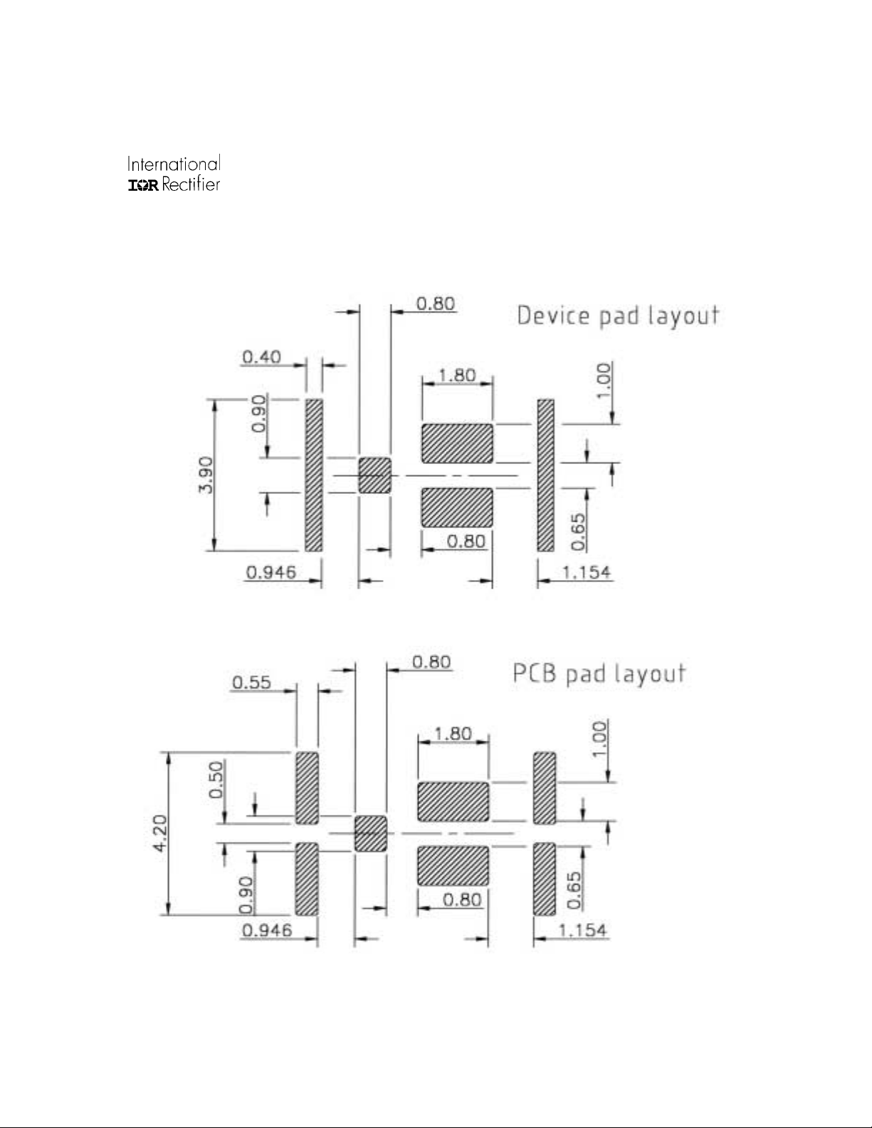
DirectFET™ Pad Layout
PROVISIONAL
IRF6603
www.irf.com 3
Page 4
IRF6603
PROVISIONAL
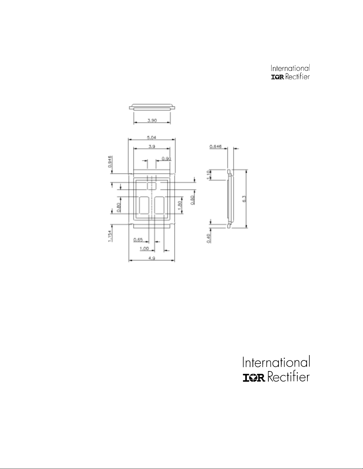
DirectFET™ Outline Dimension
Notes:
Repetitive rating; pulse width limited by
max. junction temperature.
Pulse width ≤ 400µs; duty cycle ≤ 2%.
Surface mounted on 1 in square Cu board
Used double sided cooling, mounting pad
This product has been designed and qualified for the Consumer market.
IR WORLD HEADQUARTERS: 233 Kansas St., El Segundo, California 90245, USA Tel: (310) 252-7105
Mounted on minimum footprint full size board with
metalized back and with small clip heatsink
TC measured with thermal couple mounted to top
(Drain) of part.
Data and specifications subject to change without notice.
Qualification Standards can be found on IR’s Web site.
TAC Fax: (310) 252-7903
Visit us at www.irf.com for sales contact information.01/02
4 www.irf.com
 Loading...