

Page 1
IRF630
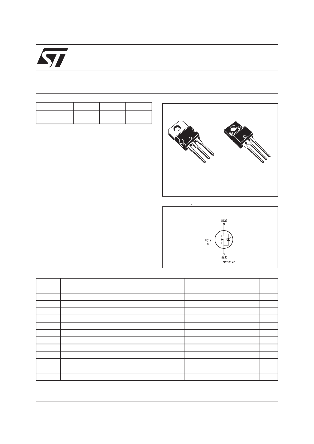
N - CHANNEL 200V - 0.35Ω - 9A - TO-220/FP
TYPE V
IRF 630
IRF 630FP
■ TYPICALR
■ EXTREMELY HIGH dV/dt CAPABILITY
■ VERYLOW INTRINSIC CAPACITANCES
■ GATECHARGE MINIMIZED
DS(on)
DSS
200 V
200 V
= 0.35 Ω
DESCRIPTION
This power MOSFET is designed using he
company’sconsolidatedstrip layout-based MESH
OVERLAYprocess. This technology matches
and improves the performances compared with
standardpartsfrom varioussources.
APPLICATIONS
■ HIGHCURRENT SWITCHING
■ UNINTERRUPTIBLE POWER SUPPLY (UPS)
■ DC/DC COVERTERSFOR TELECOM,
INDUSTRIAL,AND LIGHTINGEQUIPMENT.
R
DS(on)
<0.40Ω
<0.40Ω
I
D
9A
9A
IRF630FP
MESH OVERLAY MOSFET
3
2
1
TO-220 TO-220FP
INTERNAL SCHEMATIC DIAGRAM
3
2
1
ABSOLUTE MAXIMUM RATINGS
Symbol Parameter Value Unit
IRF63 0 IRF 630FP
V
V
V
I
DM
P
dv/dt(
V
T
(•) Pulsewidth limited by safeoperating area (1)I
First Digit of the DatecodeBeing Z or K IdentifiesSilicon Characterized in this Datasheet
(**)Limited only by Maximum TemperatureAllowed
February 1999
Dra in- sour c e Voltage (VGS= 0) 200 V
DS
Dra in- gat e Voltage (RGS=20kΩ) 200 V
DGR
Gat e-source Voltage
GS
Dra in Cu rr ent ( continuous ) a t Tc=25oC 9 9(**) A
I
D
Dra in Cu rr ent ( continuous ) a t Tc=100oC5.75.7(**)A
I
D
20 V
±
(•) Dra in Cu rr ent ( p uls ed ) 36 36 A
Tot al Dis sipation at Tc=25oC7525W
tot
Der ati ng Factor 0.6 0.20 W/
) Peak Diode Recovery voltage slope 5 5 V/ ns
1
Insulation W ithstand Voltage (DC) 20 00 V
ISO
St orage T em pe r at ure -65 to 150
stg
Max. Operating Junct ion Temperat ur e 150
T
j
≤
9A, di/dt≤300 A/µs, V
SD
≤
DD
V
(BR)DSS
,Tj≤T
JMAX
o
C
o
C
o
C
1/9
Page 2
IRF630/FP
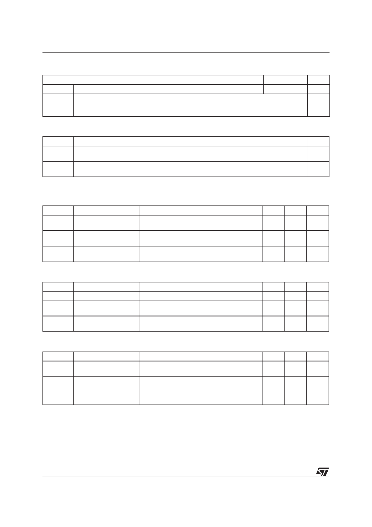
THERMAL DATA
TO-220 TO-220FP
R
thj-case
R
thj-amb
R
thc-sink
T
AVALANCHE CHARACTERISTICS
Symbol Paramet er Max Value Unit
I
AR
E
Ther mal Resistanc e Junct ion-case Ma x 1.67 4.17
Ther mal Resistanc e Junct ion-ambient Max
Ther mal Resistanc e Case-sink Ty p
Maximum Lead Te m pe ra t ure For Soldering Pur p os e
l
Avalanche Current, R epetitiv e or Not-Repetitive
(pulse width limited by T
Single Pul se Avalanc he E nergy
AS
(starting T
=25oC, ID=IAR,VDD=50V)
j
max)
j
62.5
0.5
300
9A
160 mJ
o
C/W
o
C/W
o
C/W
o
C
ELECTRICAL CHARACTERISTICS
=25oC unless otherwisespecified)
(T
case
OFF
Symbol Parameter Test Conditions Min. Typ. Max. Unit
V
(BR)DSS
Drain-source
ID=250µAVGS= 0 200 V
Break dow n Vo lt age
I
DSS
I
GSS
Zero Gate Voltage
Drain Curre nt (V
GS
Gat e- bod y Leakage
Current (V
DS
=0)
=0)
V
=MaxRating
DS
=MaxRating Tc=125oC
V
DS
V
=± 20 V
GS
1
50
100 nA
±
ON(∗)
Symbol Parameter Test Conditions Min. Typ. Max. Unit
V
GS(th)
R
DS(on)
Gate Threshold Voltage VDS=VGSID= 250µA 234V
Sta t ic Drain-s ource On
VGS=10V ID= 5 A 0.35 0.40
Resistance
I
D(on)
On State Drain Current VDS>I
D(on)xRDS(on)max
10 A
VGS=10V
DYNAMIC
Symbol Parameter Test Conditions Min. Typ. Max. Unit
g
(∗)Forward
fs
Tr ansc on duc tance
C
C
C
Input Capaci t ance
iss
Out put Capac it ance
oss
Reverse Transfer
rss
Capacit a nc e
VDS>I
D(on)xRDS(on)maxID
=5A 3 4 S
VDS=25V f=1MHz VGS= 0 540
90
35
700
120
50
µA
µA
Ω
pF
pF
pF
2/9
Page 3
IRF630/FP
ELECTRICAL CHARACTERISTICS
(continued)
SWITCHING ON
Symbol Parameter Test Conditions Min. Typ. Max. Unit
t
d(on)
t
r
Turn-on Time
Rise Time
VDD=100V ID= 4.5 A
R
=4.7
G
Ω
VGS=10V
10
15
14
20
(see test circuit, figure 3)
Q
Q
Q
Tot al Gate C harge
g
Gat e- Source Charge
gs
Gate-Drain Charge
gd
VDD= 160 V ID=9A VGS=10V 31
7.5
9
45 nC
SWITCHING OFF
Symbol Parameter Test Conditions Min. Typ. Max. Unit
t
r(Voff)
t
t
Off-voltage Rise Tim e
Fall T ime
f
Cross-over Tim e
c
VDD=160V ID=9A
=4.7 Ω VGS=10V
R
G
(see test circuit, figure 5)
12
12
25
17
17
35
SOURCEDRAINDIODE
Symbol Parameter Test Conditions Min. Typ. Max. Unit
I
SD
I
SDM
V
SD
t
Q
I
RRM
(∗) Pulsed:Pulse duration = 300µs, duty cycle 1.5%
(•) Pulse width limited by safeoperating area
Source-drain Current
(•)
Source-drain Current
9
36
(pulsed)
(∗)ForwardOnVoltage ISD=9A VGS=0 1.5 V
Reverse Recovery
rr
Time
Reverse Recovery
rr
ISD=9A di/dt=100A/µs
=50V Tj= 150oC
V
DD
(see test circuit, figure 5)
170
0.95
Charge
Reverse Recovery
11
Current
ns
ns
nC
nC
ns
ns
ns
A
A
ns
µ
A
C
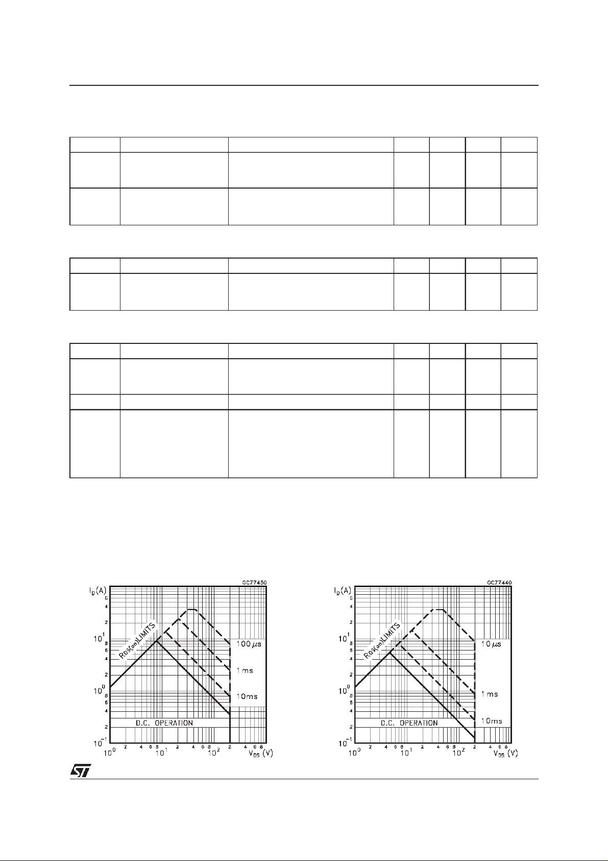
SafeOperating Area for TO-220 SafeOperating Area for TO-220FP
3/9
Page 4
IRF630/FP
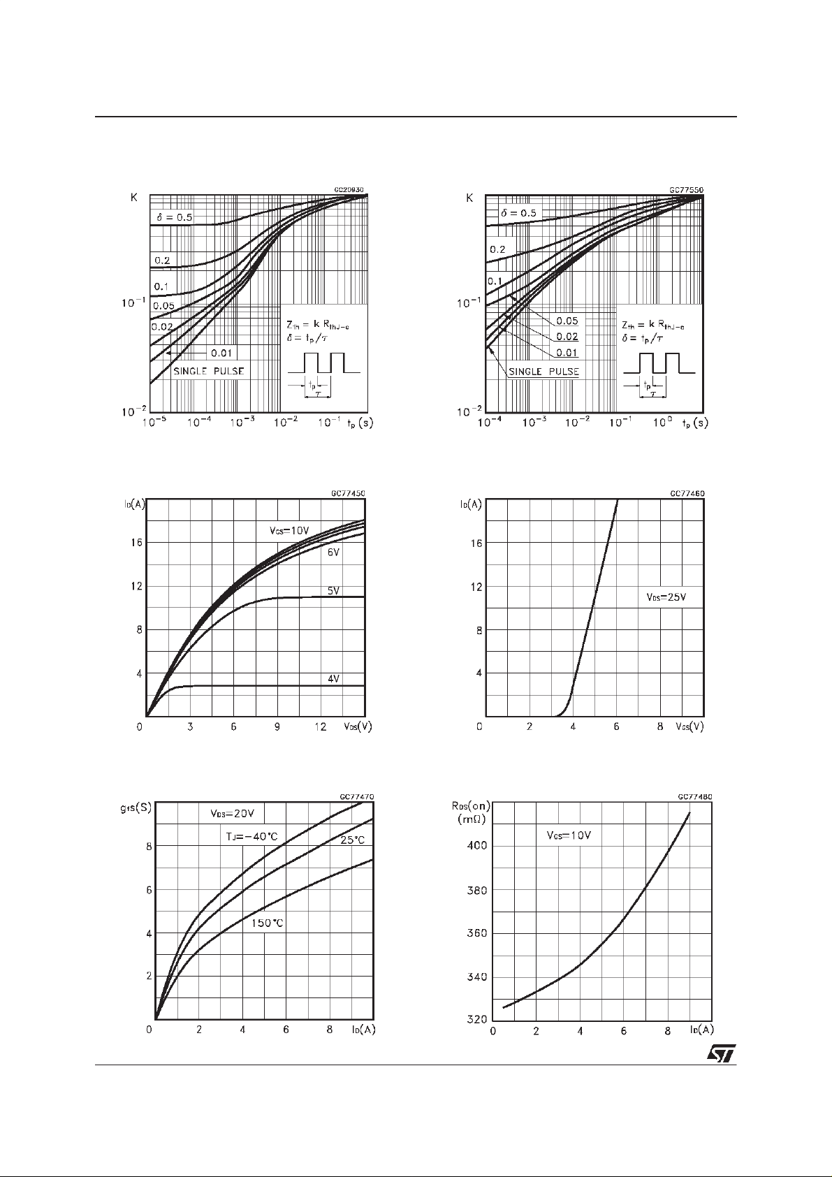
ThermalImpedancefor TO-220
OutputCharacteristics
ThermalImpedance for TO-220FP
TransferCharacteristics
Transconductance
4/9
Static Drain-sourceOn Resistance
Page 5
IRF630/FP
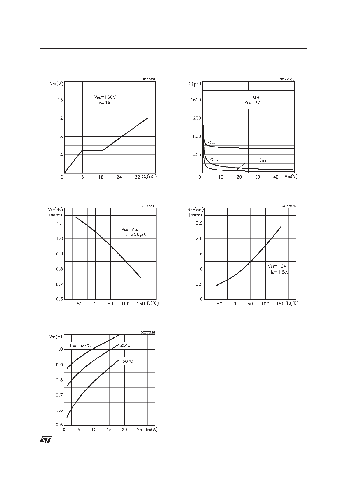
Gate Charge vs Gate-sourceVoltage
NormalizedGate ThresholdVoltage vs
Temperature
CapacitanceVariations
NormalizedOn Resistancevs Temperature
Source-drainDiode Forward Characteristics
5/9
Page 6
IRF630/FP
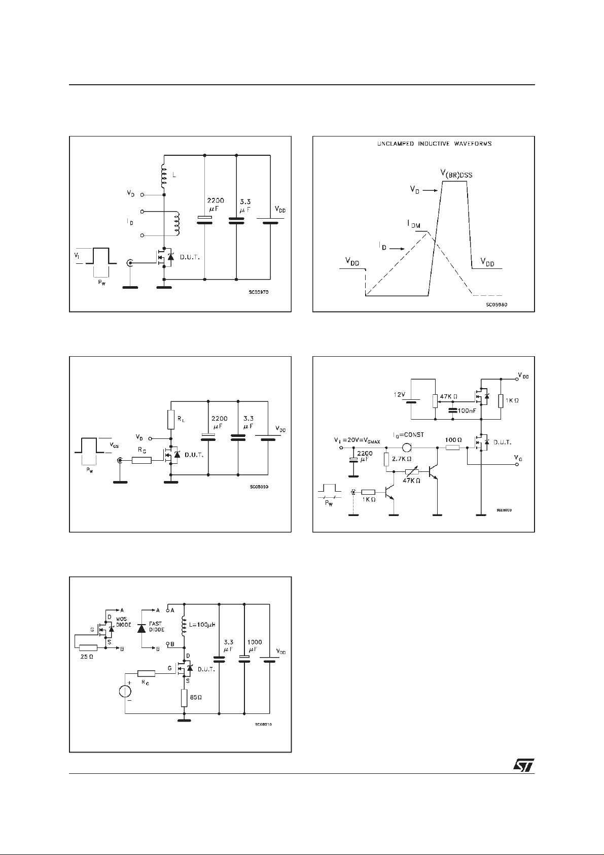
Fig. 1:
UnclampedInductiveLoad Test Circuit
Fig. 3: SwitchingTimes Test CircuitsFor
ResistiveLoad
Fig. 2:
UnclampedInductive Waveform
Fig. 4: Gate Chargetest Circuit
Fig. 5:
Test Circuit For InductiveLoad Switching
And Diode Recovery Times
6/9
Page 7
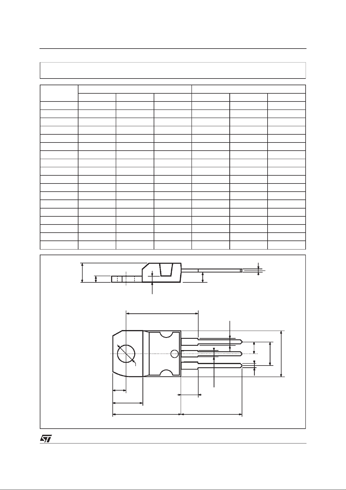
TO-220 MECHANICALDATA
IRF630/FP
DIM.
MIN. TYP. MAX. MIN. TYP. MAX.
A 4.40 4.60 0.173 0.181
C 1.23 1.32 0.048 0.051
D 2.40 2.72 0.094 0.107
D1 1.27 0.050
E 0.49 0.70 0.019 0.027
F 0.61 0.88 0.024 0.034
F1 1.14 1.70 0.044 0.067
F2 1.14 1.70 0.044 0.067
G 4.95 5.15 0.194 0.203
G1 2.4 2.7 0.094 0.106
H2 10.0 10.40 0.393 0.409
L2 16.4 0.645
L4 13.0 14.0 0.511 0.551
L5 2.65 2.95 0.104 0.116
L6 15.25 15.75 0.600 0.620
L7 6.2 6.6 0.244 0.260
L9 3.5 3.93 0.137 0.154
DIA. 3.75 3.85 0.147 0.151
mm inch
E
A
L4
D
F2
F1
G1
H2
G
F
P011C
C
D1
L2
Dia.
L5
L7
L6
L9
7/9
Page 8
IRF630/FP
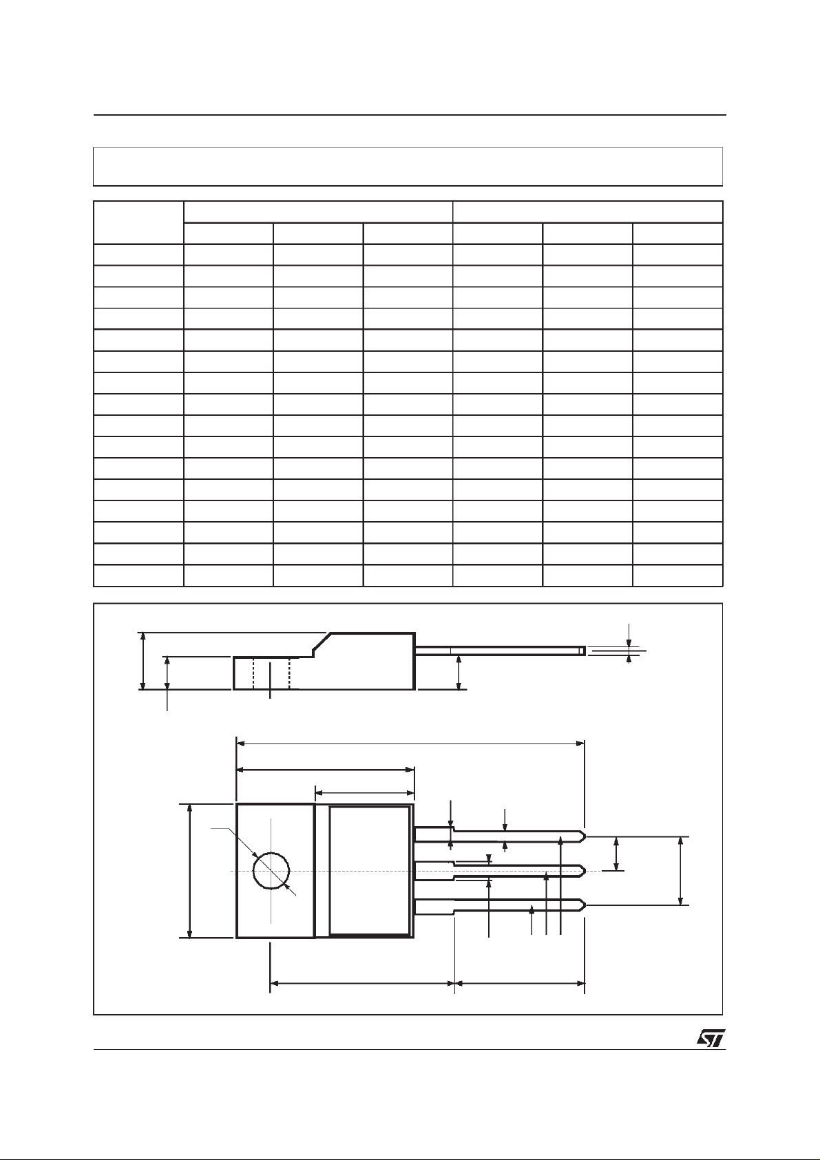
TO-220FP MECHANICAL DATA
DIM.
MIN. TYP. MAX. MIN. TYP. MAX.
A 4.4 4.6 0.173 0.181
B 2.5 2.7 0.098 0.106
D 2.5 2.75 0.098 0.108
E 0.45 0.7 0.017 0.027
F 0.75 1 0.030 0.039
F1 1.15 1.7 0.045 0.067
F2 1.15 1.7 0.045 0.067
G 4.95 5.2 0.195 0.204
G1 2.4 2.7 0.094 0.106
H 10 10.4 0.393 0.409
L2 16 0.630
L3 28.6 30.6 1.126 1.204
L4 9.8 10.6 0.385 0.417
L6 15.9 16.4 0.626 0.645
L7 9 9.3 0.354 0.366
Ø 3 3.2 0.118 0.126
mm inch
E
A
D
B
L3
L6
L7
¯
F1
F
G1
H
G
F2
123
L2
L4
8/9
Page 9

IRF630/FP
Information furnished is believed to be accurateand reliable.However, STMicroelectronics assumesno responsibilityforthe consequences
of use of such information nor for any infringement of patents or other rights of third parties which may result from its use. No license is
granted by implication orotherwise under any patent or patent rights of STMicroelectronics. Specificationmentioned in this publication are
subjecttochange without notice.Thispublication supersedes and replaces all information previouslysupplied.STMicroelectronicsproducts
are not authorized foruse as critical components in life support devicesor systemswithout express written approval of STMicroelectronics.
The STlogo is a trademark of STMicroelectronics
1999 STMicroelectronics – Printed in Italy – All Rights Reserved
STMicroelectronics GROUP OF COMPANIES
Australia - Brazil - Canada - China - France - Germany - Italy- Japan - Korea - Malaysia - Malta - Mexico- Morocco - The Netherlands -
Singapore - Spain - Sweden - Switzerland - Taiwan- Thailand - United Kingdom - U.S.A.
http://www.st.com
.
9/9
 Loading...