

Page 1
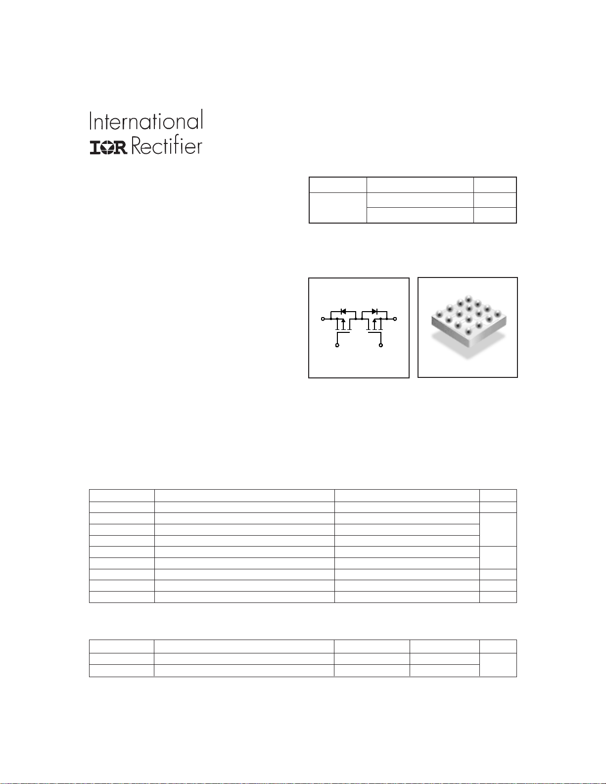
PROVISIONAL
l Ultra Low R
l Low Thermal Resistance
l Bi-Directional P-Channel Switch
l Super Low Profile (<.8mm)
l Available Tested on Tape & Reel
per Footprint Area
SS(on)
Description
True chip-scale packaging is available from International
Rectifier. Through the use of advanced processing techniques and a unique packaging concept, extremely low
on-resistance and the highest power densities in the
industry have been made available for battery and load
management applications. These benefits, combined with
the ruggedized device design that International Rectifier
is well known for,
tremely efficient and reliable device.
The FlipFET™ package, is one-third the footprint of a
comparable SO-8 package and has a profile of less than
.8mm. Combined with the low thermal resistance of the
die level device, this makes the FlipFET™ the best device
for applications where printed circuit board space is at a
premium and in extremely thin application environments
such as battery packs, cell phones and PCMCIA cards.
provides the designer with an ex-
HEXFET® Power MOSFET
V
SS
-20V 0.036Ω@V
0.052Ω@V
S1
G1
R
G2
IRF6150
max I
SS(on)
= -4.5V -7.9A
GS1,2
= -2.5V -6.3A
GS1,2
S2
PD - 93943
S
Absolute Maximum Ratings
Parameter Max. Units
V
SS
IS @ TC = 25°C Continuous Current, V
IS @ TC = 70°C Continuous Current, V
I
SM
PD @TC = 25°C Power Dissipation 3.0
PD @TC = 70°C Power Dissipation 1.9
V
GS
T
J, TSTG
Source- Source Voltage -20 V
= V
GS1
GS1
Pulsed Current ±40
Linear Derating Factor 24 mW/°C
Gate-to-Source Voltage ± 12 V
Junction and Storage Temperature Range -55 to + 150 °C
= -4.5V ±7.9
GS2
= V
= -4.5V ±6.3 A
GS2
W
Thermal Resistance
Symbol Parameter Typ. Max. Units
R
θJA
R
θJ-PCB
Junction-to-Ambient 42 °C/W
Junction-to-PCB mounted 17 –––
www.irf.com 1
6/29/00
Page 2
IRF6150
PROVISIONAL
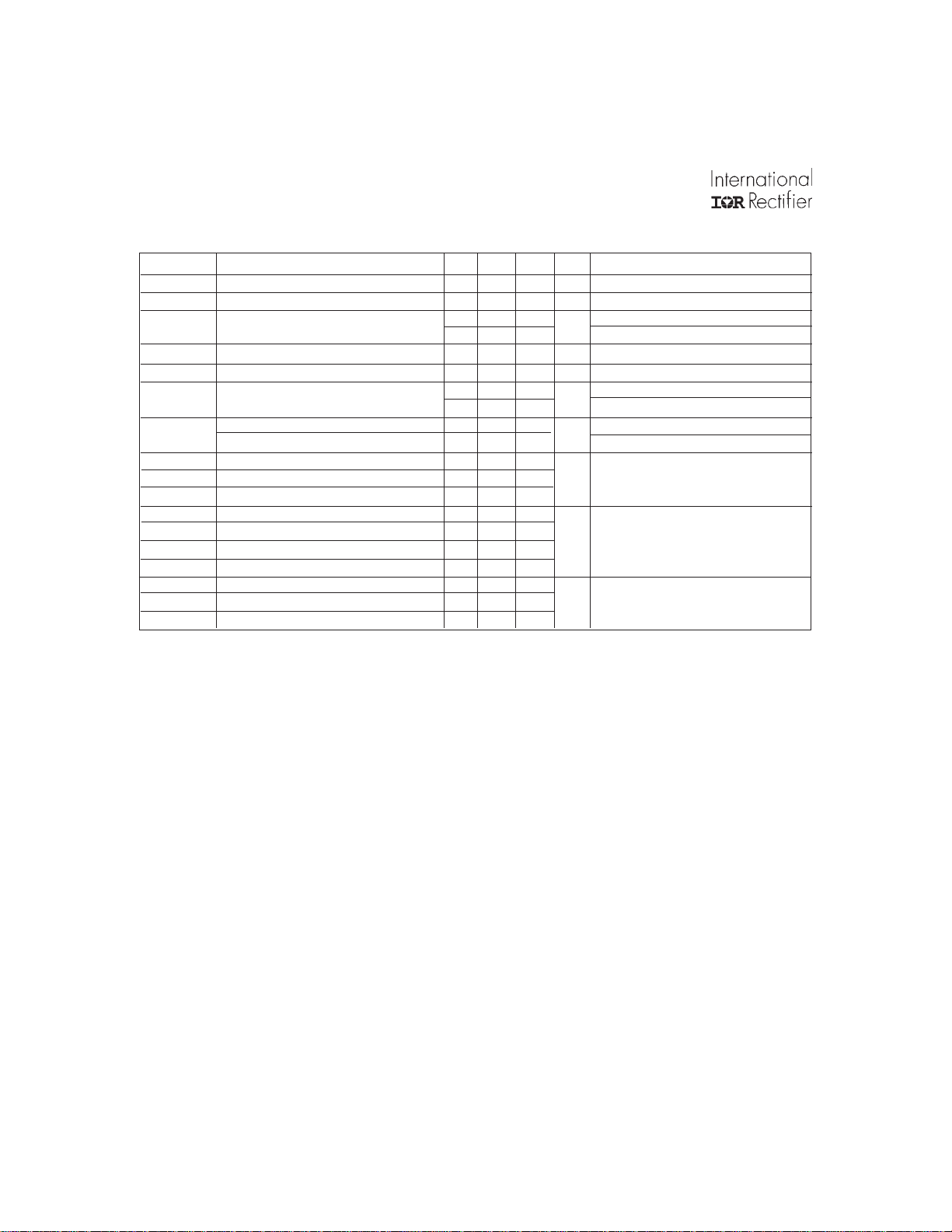
Electrical Characteristics @ TJ = 25°C (unless otherwise specified)
Parameter Min. Typ. Max. Units Conditions
V
(BR)SSS
∆V
(BR)SSS
R
SS(on)
V
GS(th)
g
fs
I
SSS
I
GSS
Q
g
Q
gs
Q
G1-S2
t
d(on)
t
r
t
d(off)
t
f
C
iss
C
oss
C
rss
Source-to-Source Breakdown Voltage -20 ––– ––– V VGS = 0V, ID = -250µA
/∆T
Breakdown Voltage Temp. Coefficient ––– -TBD –– – V/°C Reference to 25°C, ID = -1mA
J
Static Source-to-Source On-Resistance
––– ––– 0.036 V
––– ––– 0.052 V
Ω
GS1
GS1
= V
= V
GS2
GS2
Gate Threshold Voltage -0.45 ––– -1.2 V VSS = VGS, IS = -250µA
Forward Transconductance TBD ––– ––– S VSS = -10V, IS = -7.9A
Zero Gate Voltage Source Current
––– ––– -1.0
––– ––– -25 VSS = -16V, VGS = 0V, TJ = 125°C
Gate-to-Source Forward Leakage ––– ––– 100 VGS = 12V
Gate-to-Source Reverse Leakage ––– ––– -100
VSS = -20V, VGS = 0V
µA
nA
VGS = -12V
Total Gate Charge ––– TBD T B D IS = -TBDA
Gate-to-Source Charge ––– TBD TBD nC VSS = -16V
Miller Charge ––– TBD TBD VGS = -5.0V
Turn-On Delay Time ––– TB D ––– VSS = -10V
Rise Time ––– TBD ––– IS = -1.0A
Turn-Off Delay Time ––– TBD ––– RG = 6.0Ω
ns
Fall Time ––– TBD ––– VGS = -5.0V
Input Capacitance ––– TBD ––– VGS = 0V
Output Capacitance ––– TBD ––– pF VSS = -15V
Reverse Transfer Capacitance ––– TBD ––– ƒ = 1.0MHz
= -4.5V, IS = -7.9A
= -2.5V, IS = -6.3A
Notes:
Repetitive rating; pulse width limited by
max. junction temperature.
Pulse width ≤ 400µs; duty cycle ≤ 2%. Gate voltage applied to both gates.
When mounted on 1 inch square 2oz copper on FR-4
2 www.irf.com
Page 3
PROVISIONAL
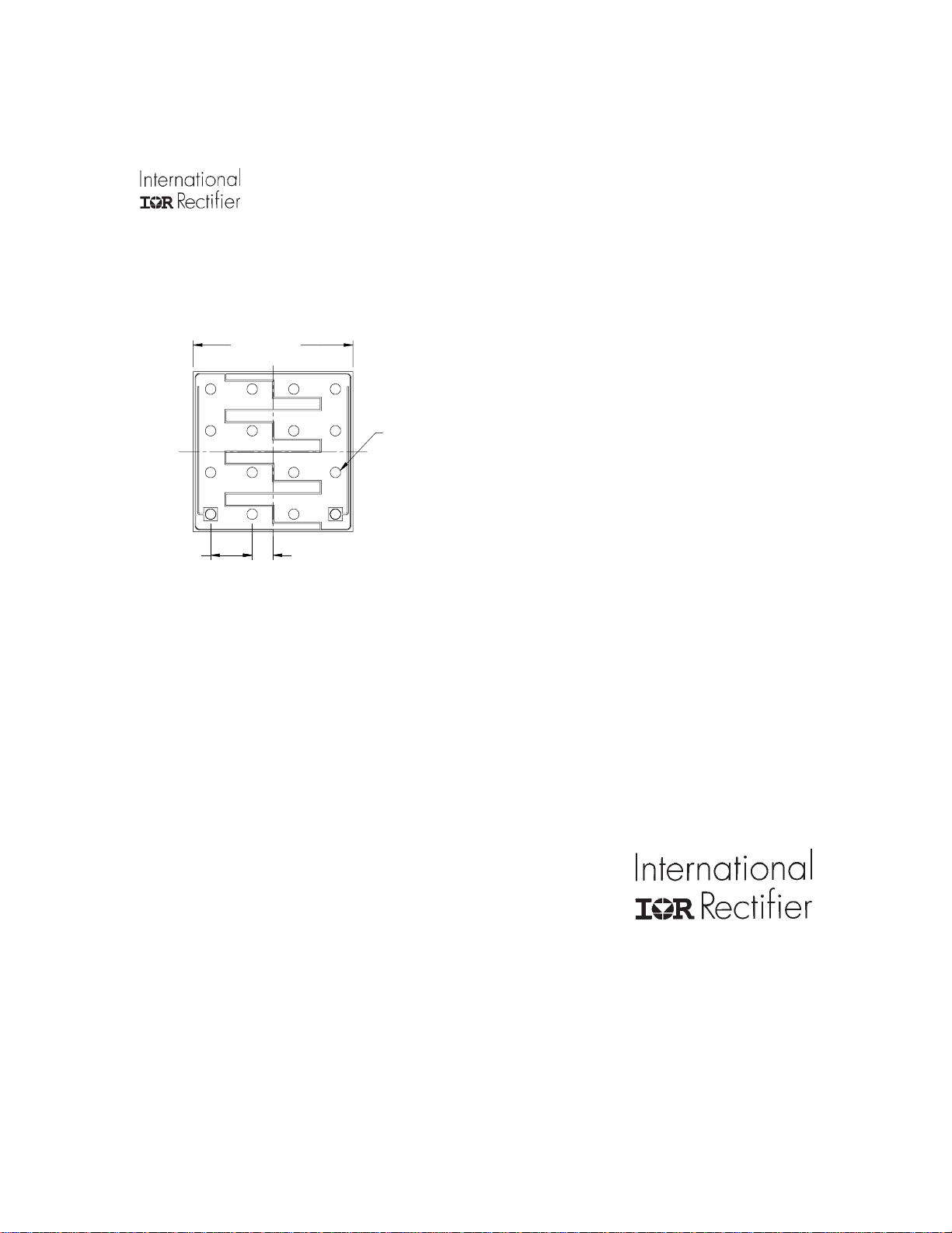
Bi-Directional MOSFET Outline Dimension
NOTES :
3.124
2X
[.123]
S1 S1 S2 S2
16X Ø
0.20
[.008]
0.80
[.032]
S1
G1 S 1
S1 S2 S2
S2 G2
0.40
4X4X
[.016]
S2S2S1S1
IRF6150
1. ALL DIMENSIONS ARE SHO WN IN MILLIMETERS [INCHES].
2. CONTROLLING DIMENSION: [INCH].
3. LETTER DES IGNATION:
S = SOURCE
G = GAT E
4. DIMENSIONA L TOLERAN CES:
BONDING PADS:
OVERALL DIE:
5. UNLESS OTHERWISE NOTED ALL DIE ARE GEN III
WIDT H
&
LENGTH
WIDT H
&
SK = SOUR CE KE LVIN
IS = CU RR ENTSENSE
< 0.635 TOLERANCE = + / - 0.0 13
< [.0250] TO LERANCE = + /- [.0005]
> 0.635 TOLERANCE = + / - 0.0 25
> [.0250] TO LERANCE = + /- [.0010]
< 1.270 TOLERANCE = + /- 0.102
< [.050] TOLERANCE = + /- [.004]
> 1.270 TOLERANCE = + /- 0.203
> [.050] TOLERANCE = + /- [.008]LENGTH
E = EMITTER
IR EUROPEAN REGIONAL CENTRE: 439/445 Godstone Rd, Whyteleafe, Surrey CR3 OBL, UK Tel: ++ 44 (0)20 8645 8000
IR WORLD HEADQUARTERS: 233 Kansas St., El Segundo, California 90245, USA Tel: (310) 252-7105
IR CANADA: 15 Lincoln Court, Brampton, Ontario L6T3Z2, Tel: (905) 453 2200
IR GERMANY: Saalburgstrasse 157, 61350 Bad Homburg Tel: ++ 49 (0) 6172 96590
IR ITALY: Via Liguria 49, 10071 Borgaro, Torino Tel: ++ 39 011 451 0111
IR JAPAN: K&H Bldg., 2F, 30-4 Nishi-Ikebukuro 3-Chome, Toshima-Ku, Tokyo 171 Tel: 81 (0)3 3983 0086
IR SOUTHEAST ASIA: 1 Kim Seng Promenade, Great World City West Tower, 13-11, Singapore 237994 Tel: ++ 65 (0)838 4630
IR TAIWAN:16 Fl. Suite D. 207, Sec. 2, Tun Haw South Road, Taipei, 10673 Tel: 886-(0)2 2377 9936
Data and specifications subject to change without notice.6/00
www.irf.com 3
 Loading...