

Page 1
PD-93998A
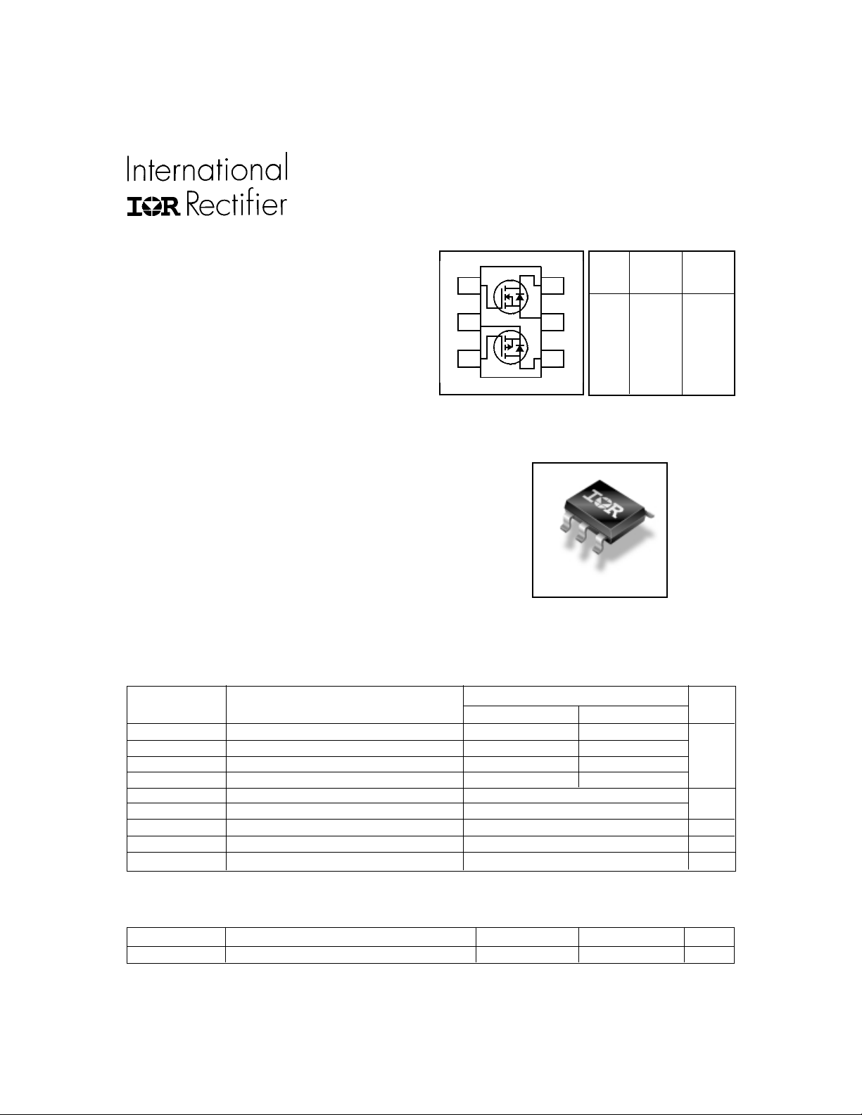
IRF5851
HEXFET® Power MOSFET
l Ultra Low On-Resistance
l Dual N and P Channel MOSFET
l Surface Mount
l Available in Tape & Reel
l Low Gate Charge
Description
These N and P channel MOSFETs from International
Rectifier utilize advanced processing techniques to achieve
the extremely low on-resistance per silicon area. This
benefit provides the designer with an extremely efficient
device for use in battery and load management
applications.
This Dual TSOP-6 package is ideal for applications
where printed circuit board space is at a premium and
where maximum functionality is required. With two die
per package, the IRF5851 can provide the functionality of
two SOT-23 packages in a smaller footprint. Its unique
thermal design and R
increase in current-handling capability.
reduction enables an
DS(on)
G1
S2
G2
N-Ch P-Ch
1
2
3
D1
6
V
S1
5
D2
4
R
DS(on)
TSOP-6
20V -20V
DSS
0.090Ω 0.135Ω
Absolute Maximum Ratings
Parameter
V
DS
ID @ TA = 25°C Continuous Drain Current, VGS @ 10V 2.7 -2.2
ID @ TA = 70°C Continuous Drain Current, VGS @ 10V 2.2 -1.7
I
DM
PD @TA = 25°C Power Dissipation 0.96 W
PD @TA = 70°C Power Dissipation 0.62
V
GS
T
J, TSTG
Drain-to-Source Voltage 20 -20
Pulsed Drain Current 11 -9.0
Linear Derating Factor 7.7 mW/°C
Gate-to-Source Voltage ± 12 V
Junction and Storage Temperature Range °C
N-Channel P-Channel
Max.
-55 to + 150
Units
A
Thermal Resistance
Parameter Typ. Max. Units
R
θJA
Maximum Junction-to-Ambient ––– 130 °C/W
www.irf.com 1
2/26/02
Page 2
IRF5851
Electrical Characteristics @ TJ = 25°C (unless otherwise specified)
V
(BR)DSS
∆V
(BR)DSS
R
DS(ON)
V
GS(th)
g
fs
I
DSS
I
GSS
Q
g
Q
gs
Q
gd
t
d(on)
t
r
t
d(off)
t
f
C
iss
C
oss
C
rss
Drain-to-Source Breakdown Voltage
/∆TJBreakdown Voltage Temp. Coefficient
Static Drain-to-Source On-Resistance
Gate Threshold Voltage
Forward Transconductance
Drain-to-Source Leakage Current
Gate-to-Source Forward Leakage N-P –– — ±100 VGS = ± 12V
Total Gate Charge
Gate-to-Source Charge
Gate-to-Drain ("Miller") Charge
Turn-On Delay Time
Rise Time
Turn-Off Delay Time
Fall Time
Input Capacitance
Output Capacitance
Reverse Transfer Capacitance
Parameter Min. Typ. Max. Units Conditions
N-Ch 20 —— VGS = 0V, ID = 250µA
P-Ch -20 —— V
N-Ch — 0.016 — Reference to 25°C, I
P-Ch — -0.011 — Reference to 25°C, I
——0.090 VGS = 4.5V, ID = 2.7A
N-Ch
——0.120 V
——0.135 V
P-Ch
——0.220 V
N-Ch 0.60 — 1.25 V
P-Ch -0.45 — -1.2 VDS = VGS, ID = -250µA
N-Ch 5.2 —— VDS = 10V, ID = 2.7A
P-Ch 3.5 —— V
N-Ch ——1.0 VDS = 16 V , VGS = 0V
P-Ch ——-1.0 VDS = -16V, VGS = 0V
N-Ch ——25 V
P-Ch ——-25 VDS = -16V, VGS = 0V, TJ = 70°C
N-Ch — 4.0 6.0
P-Ch — 3.6 5.4
N-Ch — 0.95 —
P-Ch — 0.66 —
N-Ch — 0.83 —
P-Ch — 5.7 —
N-Ch — 6.6 —
P-Ch — 8.3 —
N-Ch — 1.2 —
P-Ch — 14 —
N-Ch — 15 —
P-Ch — 31 —
N-Ch — 2.4 —
P-Ch — 28 —
N-Ch — 400 —
P-Ch — 320 —
N-Ch — 48 —
P-Ch — 56 —
N-Ch — 32 —
P-Ch — 40 —
V
= 0V, ID = -250µA
GS
V/°C
= 2.5V, ID = 2.2A
GS
Ω
= -4.5V, ID = -2.2A
GS
= -2.5V, ID = -1.7A
GS
= VGS, ID = 250µA
DS
V
S
= -10V, ID = -2.2A
DS
µA
= 16 V , VGS = 0V, TJ = 70°C
DS
N-Channel
= 2.7A, VDS = 10V, VGS = 4.5V
I
D
nC
P-Channel
ID = -2.2A, VDS = -10V, VGS = -4.5V
N-Channel
= 10V, ID = 1.0A, RG = 6.2Ω,
V
DD
VGS = 4.5V
ns
P-Channel
VDD = -10V, ID = -1.0A, RG = 6.0Ω,
VGS = -4.5V
N-Channel
= 0V, VDS = 15V, ƒ = 1.0MHz
V
GS
pF
P-Channel
VGS = 0V, VDS = -15V, ƒ = 1.0MHz
= 1mA
D
= -1mA
D
Source-Drain Ratings and Characteristics
Parameter Min. Typ. Max. Units Conditions
I
S
I
SM
V
SD
t
rr
Q
rr
Continuous Source Current (Body Diode)
Pulsed Source Current (Body Diode)
Diode Forward Voltage
Reverse Recovery Time
Reverse Recovery Charge
Notes:
Repetitive rating; pulse width limited by
max. junction temperature. ( See fig. 10 & 26 )
Pulse width ≤ 400µs; duty cycle ≤ 2%.
N-Ch ——0.96
P-Ch ——-0.96
N-Ch ——11
A
P-Ch ——-9.0
N-Ch ——1.2 T
P-Ch ——-1.2 TJ = 25°C, IS = -0.96A, VGS = 0V
N-Ch — 25 38
P-Ch — 23 35
N-Ch — 6.5 9.8
P-Ch — 7.7 12
= 25°C, IS = 0.96A, VGS = 0V
J
V
N-Channel
ns
T
= 25°C, IF = 0.96A, di/dt = 100A/µs
J
P-Channel
nC
T
= 25°C, IF = -0.96A, di/dt = -100A/µs
J
Surface mounted on FR-4 board, t ≤ 10sec.
2 www.irf.com
Page 3
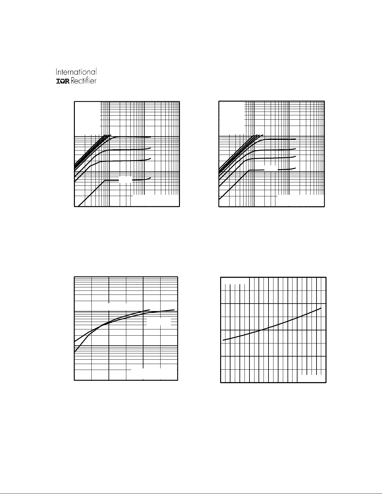
N-Channel
IRF5851
100
10
1
TOP
BOTTOM
VGS
7.5V
4.5V
3.5V
3.0V
2.5V
2.0V
1.75V
1.5V
1.50V
D
I , Drain-to-Source Current (A)
20µs PULSE WIDTH
°
T = 25 C
0.1
0.1 1 10 100
V , Drain-to-Source Voltage (V)
DS
J
Fig 1. Typical Output Characteristics
100
100
10
1
D
I , Drain-to-Source Current (A)
0.1
0.1 1 10 100
VGS
TOP
7.5V
4.5V
3.5V
3.0V
2.5V
2.0V
1.75V
BOTTOM
1.5V
1.50V
20µs PULSE WIDTH
T = 150 C
J
V , Drain-to-Sou rce Voltage (V)
DS
°
Fig 2. Typical Output Characteristics
2.0
I =
D
2.7A
°
T = 25 C
10
1
D
I , Drain-to-Source Current (A)
0.1
1.5 2.0 2.5 3.0
V , Gate-to-Source Voltage (V)
GS
J
T = 150 C
J
V = 15V
DS
20µs PULSE WIDTH
Fig 3. Typical Transfer Characteristics
°
1.5
1.0
(Normalized)
0.5
DS(on)
R , Drain-to-Source On Resistance
0.0
-60 -40 -20 0 20 40 60 80 100 120 140 160
T , Junction Temperature( C)
J
Fig 4. Normalized On-Resistance
V =
GS
°
4.5V
Vs. Temperature
www.irf.com 3
Page 4
IRF5851
N-Channel
600
500
400
300
200
C, Capacitance (pF)
100
0
1 10 100
V
=
0V,
GS
C
=
iss gs gd , ds
C
=
rss gd
C
=
oss ds gd
C
iss
C
oss
C
rss
V , Drain-to-Source Voltage (V)
DS
f = 1MHz
C
+ C
C
C
C SHORTED
+ C
Fig 5. Typical Capacitance Vs.
Drain-to-Source Voltage
100
10
I =
2.7A
D
8
6
4
2
GS
V , Gate-to-Source Voltage (V)
0
0 2 4 6 8
Q , Total Gate Charge (nC)
G
V = 16V
DS
V = 10V
DS
Fig 6. Typical Gate Charge Vs.
Gate-to-Source Voltage
100
OPERATION IN THIS ARE A LIMITED
BY R
DS(on)
10
°
T = 150 C
J
1
°
SD
I , Reverse Drain Current (A)
0.1
0.4 0.6 0.8 1.0 1.2 1.4
V ,Source-to-Drain Voltage (V)
SD
T = 25 C
J
V = 0 V
GS
Fig 7. Typical Source-Drain Diode
10
100us
1
D
I , Drain Current (A)I , Drain Current (A)
°
= 25 C
A
T T= 150 C
Single Pulse
0.1
0.1 1 10 100
°
J
V , Drain-to-Sou rce Voltage (V)
DS
1ms
10ms
Fig 8. Maximum Safe Operating Area
Forward Voltage
4 www.irf.com
Page 5
N-Channel
IRF5851
3.0
2.5
2.0
1.5
1.0
D
I , Drain Current (A)
0.5
0.0
25 50 75 100 125 150
T , Case Temperature ( C)
C
Fig 9. Maximum Drain Current Vs.
Case Temperature
1000
R
D.U.T.
D
+
V
DD
-
V
DS
V
GS
R
G
4.5V
Pulse Width ≤ 1 µs
Duty Factor ≤ 0.1 %
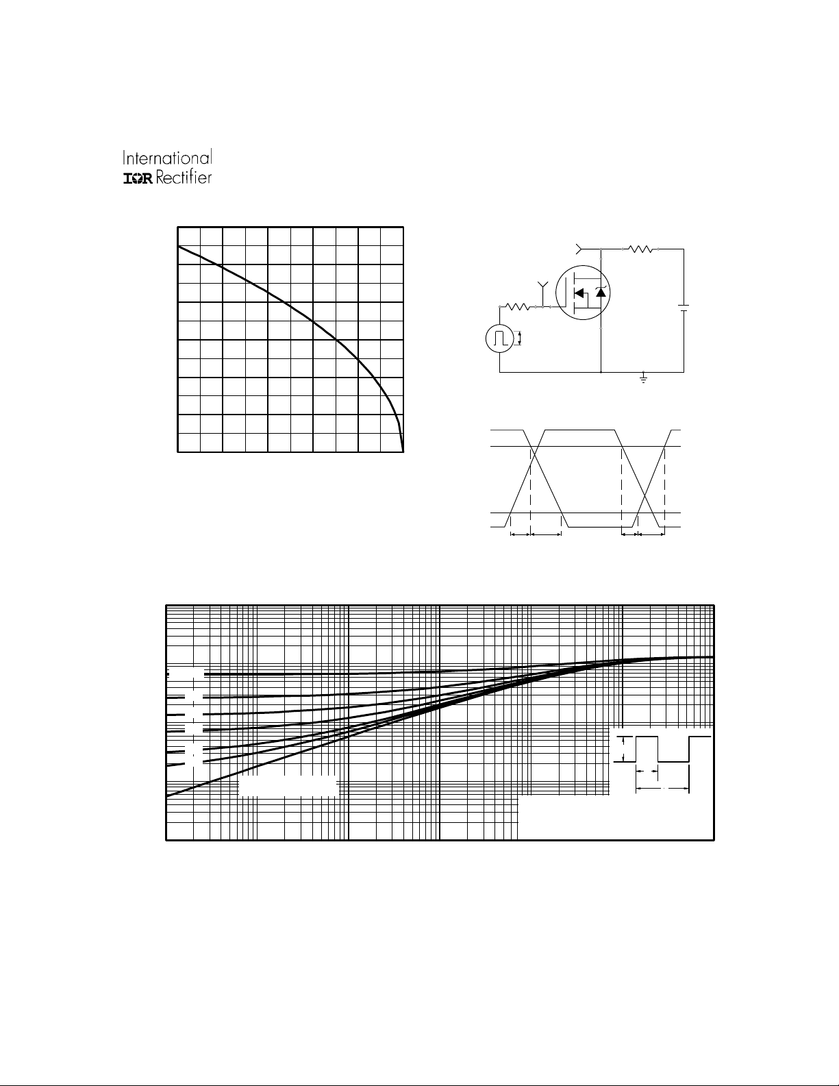
Fig 10a. Switching Time Test Circuit
V
DS
90%
°
10%
V
GS
t
d(on)tr
t
d(off)tf
Fig 10b. Switching Time Waveforms
100
thJA
D = 0.50
0.20
0.10
10
0.05
P
1 2
DM
t
1
t
2
0.02
0.01
1
Thermal R esponse (Z )
0.1
0.00001 0.0001 0.001 0.01 0.1 1 10
SINGLE PULSE
(THERMAL RESPONSE)
Notes:
1. Duty factor D = t / t
2. Peak T =P x Z + T
t , Rectangular Pulse Durati on (sec)
1
J DM thJA A
Fig 10. Typical Effective Transient Thermal Impedance, Junction-to-Ambient
www.irf.com 5
Page 6

IRF5851
)
0.14
Ω
(
e
c
n
a
t
s
i
s
0.12
e
R
n
O
e
c
r
u
0.10
o
S
o
t
-
n
i
a
r
0.08
D
,
)
n
o
(
S
D
0.06
R
2.0 3.0 4.0 5.0 6.0 7.0 8.0
V
GS,
ID = 2.7A
Gate -to - Source Voltage (V)
N-Channel
)
Ω
(
e
c
n
a
t
s
i
s
e
R
n
O
e
c
r
u
o
S
-
o
t
-
n
i
a
r
D
,
)
n
o
(
S
D
R
0.30
0.20
V
= 2.5V
GS
0.10
V
= 4.5V
GS
0.00
024681012
ID , Drain Current (A)
Fig 11. Typical On-Resistance Vs. Gate
Voltage
Q
G
4.5 V
Q
GS
V
G
Q
GD
Charge
Fig 13a. Basic Gate Charge Waveform
Fig 12. Typical On-Resistance Vs. Drain
Current
Current Regulator
Same Type as D.U.T.
50KΩ
.2µF
12V
V
GS
.3µF
D.U.T.
3mA
I
G
Current Sampling Resistors
+
V
DS
-
I
D
Fig 13b. Gate Charge Test Circuit
6 www.irf.com
Page 7

N-Channel
IRF5851
1.2
)
1.0
V
(
e
c
a
i
r
a
0.8
V
,
)
h
t
(
S
G
V
0.6
0.4
-75 -50 -25 0 25 50 75 100 125 150
TJ , Temperature ( °C )
ID = 250µA
Fig 14. Threshold Voltage Vs. Tempera-
ture
24
20
16
)
W
(
r
12
e
w
o
P
8
4
0
0.001 0.010 0.100 1.000 10.000
Time (sec)
Fig 15. Typical Power Vs. Time
www.irf.com 7
Page 8

IRF5851
P-Channel
100
10
1
0.1
D
-I , Drain-to-Source Current (A)
0.01
0.1 1 10 100
VGS
TOP
-7.0V
-5.0V
-4.5V
-2.5V
-2.0V
-1.8V
-1.5V
BOTTOM
-1.2V
-1.2V
20µs PULSE WIDTH
T = 25 C
J
-V , Drain-to-Sou rce Voltage (V)
DS
°
Fig 16. Typical Output Characteristics
10
°
T = 25 C
J
100
10
1
D
-I , Drain-to-Source Current (A)
0.1
0.1 1 10 100
VGS
TOP
-7.0V
-5.0V
-4.5V
-2.5V
-2.0V
-1.8V
-1.5V
BOTTOM
-1.2V
-1.2V
-V , Drain-to-Sou rce Voltage (V)
DS
20µs PULSE WIDTH
T = 150 C
J
°
Fig 17. Typical Output Characteristics
2.0
I =
D
-2.2A
°
T = 150 C
J
1
1.5
1.0
(Normalized)
D
-I , Drain-to-Source Current (A)
V = -15V
DS
0.1
1.2 1.6 2.0 2.4 2.8
-V , Gate-to-Source Voltage (V)
GS
20µs PULSE WIDTH
Fig 18. Typical Transfer Characteristics
0.5
DS(on)
R , Drain-to-Source On Resistance
0.0
-60 -40 -20 0 20 40 60 80 100 120 140 160
T , Junction Temperature ( C)
J
Fig 19. Normalized On-Resistance
V =
GS
°
-4.5V
Vs. Temperature
8 www.irf.com
Page 9

P-Channel
IRF5851
500
400
300
200
V
=
0V,
GS
C
=
C
iss gs gd , ds
C
=
C
rss gd
C
=
C
oss ds gd
C
iss
f = 1MHz
+ C
+ C
C SHORTED
C, Capacitance (pF)
100
C
oss
C
rss
0
1 10 100
-V , Drain-to-Source Voltage (V)
DS
Fig 20. Typical Capacitance Vs.
Drain-to-Source Voltage
10
10
I =
-2.2A
D
8
6
4
2
GS
-V , Gate-to-Source Voltage (V)
0
0 2 4 6 8
Q , Total Gate Charge (nC)
G
V =-16V
DS
V =-10V
DS
Fig 21. Typical Gate Charge Vs.
Gate-to-Source Voltage
100
OPERATION IN THIS AREA LIMITED
BY R
DS(on)
°
T = 150 C
J
1
°
T = 25 C
J
SD
-I , Reverse Drain Current (A)
V = 0 V
0.1
0.4 0.6 0.8 1.0 1.2 1.4
-V ,Source-to-Drain Voltage (V)
SD
GS
Fig 22. Typical Source-Drain Diode
10
100us
1
D
-I , Drain Current (A)I , Drain Current (A)
°
= 25 C
A
T T= 150 C
Single Pulse
0.1
0.1 1 10 100
°
J
-V , Drain-to-Source Voltage (V)
DS
1ms
10ms
Fig 23. Maximum Safe Operating Area
Forward Voltage
www.irf.com 9
Page 10

IRF5851
P-Channel
2.5
2.0
1.5
1.0
D
-I , Drain Current (A)
0.5
0.0
25 50 75 100 125 150
TJ , Junction Temperature (°C)
Fig 24. Maximum Drain Current Vs.
Junction Temperature
1000
R
D.U.T.
D
-
+
V
V
DS
V
GS
R
G
V
GS
Pulse Width ≤ 1 µs
Duty Factor ≤ 0.1 %
Fig 25a. Switching Time Test Circuit
V
10%
90%
V
GS
DS
t
d(on)tr
t
d(off)tf
Fig 25b. Switching Time Waveforms
DD
100
thJA
D = 0.50
0.20
0.10
10
0.05
P
1 2
DM
t
1
t
2
0.02
0.01
1
Thermal R esponse (Z )
0.1
0.00001 0.0001 0.001 0.01 0.1 1 10
SINGLE PULSE
(THERMAL RESPONSE)
Notes:
1. Duty factor D = t / t
2. Peak T =P x Z + T
t , Rectangular Pulse Durati on (sec)
1
J DM thJA A
Fig 26. Typical Effective Transient Thermal Impedance, Junction-to-Ambient
10 www.irf.com
Page 11

)
0.24
Ω
(
e
c
n
a
t
s
i
s
0.20
e
R
n
O
e
c
r
u
0.16
o
S
o
t
-
n
i
a
r
0.12
D
,
)
n
o
(
S
D
0.08
R
2.0 3.0 4.0 5.0 6.0 7.0
-V
Gate -to - Source Voltage (V)
GS,
ID = -2.2A
P-Channel
)
Ω
(
e
c
n
a
t
s
i
s
e
R
n
O
e
c
r
u
o
S
-
o
t
-
n
i
a
r
D
,
)
n
o
(
S
D
R
IRF5851
0.40
0.30
V
= -2.5V
GS
0.20
V
= -4.5V
GS
0.10
0246810
-ID , Drain Current (A)
Fig 27. Typical On-Resistance Vs. Gate
Voltage
Q
G
Q
GS
V
G
Q
GD
Charge
Fig 29a. Basic Gate Charge Waveform
Fig 28. Typical On-Resistance Vs. Drain
Current
Current Regulator
Same Type as D.U.T.
50KΩ
.2µF
12V
V
GS
.3µF
D.U.T.
-3mA
I
G
Current Sampling Resistors
V
DS
+
I
D
Fig 29b. Gate Charge Test Circuit
www.irf.com 11
Page 12

IRF5851
P-Channel
1.0
)
V
(
0.8
e
c
a
i
r
a
V
,
)
h
t
(
S
0.6
G
V
-
0.4
-75 -50 -25 0 25 50 75 100 125 150
TJ , Temperature ( °C )
ID = -250µA
Fig 30. Threshold Voltage Vs. Temperature
24
20
16
)
W
(
r
12
e
w
o
P
8
4
0
0.001 0.010 0.100 1.000 10.000
Time (sec)
Fig 31. Typical Power Vs. Time
12 www.irf.com
Page 13

TSOP-6 Package Outline
IRF5851
TSOP-6 Part Marking Information
EXAMPLE: THIS IS AN SI3443DV
PART NUMBER
WAFER L OT
NUMBER CODE
PA RT NUMBER C ODE REFERENC E:
3A = SI3443DV
3B = IRF5800
3C = IRF5850
3D = IRF5851
3E = IRF5852
3I = IRF5805
3J = IRF 5806
DATE CODE EXAMPLES :
YWW = 9603 = 6C
YW W = 9632 = FF
3A
XXXX
BOTTOM
YW
TOP
www.irf.com 13
WW = (1 -2 6) IF PRECEDED BY LAST DI GIT O F CALENDAR YE AR
WORK
DATE
CODE
2005
5
1996
6
1997
7
1998
8
9
1999
2000
0
WW = (27- 52) IF PRE CEDED BY A LETTER
Y
E
2005
F
1996
G
1997
H
1998
1999
J
K
2000
WE E K
WORK
WE E K
01
02
03
04
24
25 Y
26 Z
27
28
29
30
50
51 Y
WYEAR Y
A2001 1
B2002 2
C2003 3
D2004 4
X
WYEAR
A2001 A
B2002 B
C2003 C
D2004 D
X
Page 14

IRF5851
TSOP-6 Tape & Reel Information
Data and specifications subject to change without notice.
This product has been designed and qualified for the consumer market.
Qualification Standards can be found on IR’s Web site.
IR WORLD HEADQUARTERS: 233 Kansas St., El Segundo, California 90245, USA Tel: (310) 252-7105
TAC Fax: (310) 252-7903
Visit us at www.irf.com for sales contact information. 2/02
14 www.irf.com
 Loading...