

Page 1
l Ultra Low On-Resistance
l P-Channel MOSFET
l Surface Mount
l Available in Tape & Reel
l Low Gate Charge
PD -94029
IRF5805
HEXFET® Power MOSFET
V
DSS
-30V 0.098@VGS = -10V -3.8A
R
max I
DS(on)
D
0.165@VGS = -4.5V -3.0A
Description
These P-channel MOSFETs from International Rectifier
1
D
A
6
D
utilize advanced processing techniques to achieve the
extremely low on-resistance per silicon area. This
benefit provides the designer with an extremely efficient
device for use in battery and load management
applications.
The TSOP-6 package with its customized leadframe
produces a HEXFET
®
power MOSFET with R
DS(on)
D
G
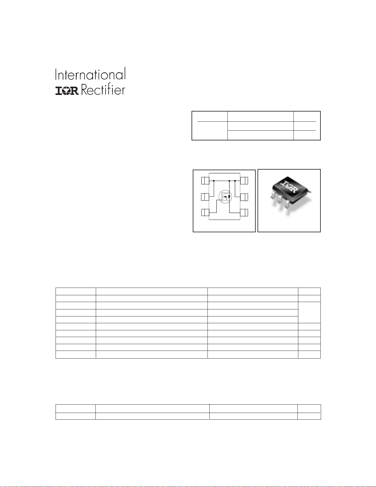
2
3
Top V iew
5
D
4
S
TSOP-6
60% less than a similar size SOT-23. This package is
ideal for applications where printed circuit board space
is at a premium. It's unique thermal design and R
DS(on)
reduction enables a current-handling increase of nearly
300% compared to the SOT-23.
Absolute Maximum Ratings
Parameter Max. Units
V
DS
ID @ TA = 25°C Continuous Drain Current, VGS @ -10V -3.8
ID @ TA = 70°C Continuous Drain Current, VGS @ -10V -3.0 A
I
DM
PD @TA = 25°C Maximum Power Dissipation 2W
P
= 70°C Maximum Power Dissipation 1.28 W
D @TA
Linear Derating Factor 0.02 W/°C
V
GS
TJ , T
STG
Drain-Source Voltage -30 V
Pulsed Drain Current -15
Gate-to-Source Voltage ± 20 V
Junction and Storage Temperature Range -55 to + 150 °C
Thermal Resistance
Parameter Max. Units
R
θJA
Maximum Junction-to-Ambient 62.5 °C/W
www.irf.com 1
11/6/00
Page 2
IRF5805
Electrical Characteristics @ TJ = 25°C (unless otherwise specified)
Parameter Min. Typ. Max. Units Conditions
V
(BR)DSS
∆V
(BR)DSS
R
DS(on)
V
GS(th)
g
fs
I
DSS
I
GSS
Q
g
Q
gs
Q
gd
t
d(on)
t
r
t
d(off)
t
f
C
iss
C
oss
C
rss
Drain-to-Source Breakdown Voltage -30 –– – –– – V VGS = 0V, ID = -250µA
/∆T
Breakdown Voltage Temp. Coefficient ––– 0.02 ––– V/°C Reference to 25°C, ID = -1mA
J
Static Drain-to-Source On-Resistance
––– ––– 0.098 VGS = -10V, ID = -3.8A
––– ––– 0.165 VGS = -4.5V, ID = -3.0A
Ω
Gate Threshold Voltage -1.0 ––– -2.5 V VDS = VGS, ID = -250µA
Forward Transconductance 3.5 ––– ––– S VDS = -10V, ID = -3.8A
Drain-to-Source Leakage Current
Gate-to-Source Forward Leakage ––– ––– -100 VGS = -20V
Gate-to-Source Reverse Leakage ––– ––– 100 VGS = 20V
––– ––– -15 VDS = -24V, VGS = 0V
––– ––– -25 VDS = -24V, VGS = 0V, TJ = 70°C
µA
nA
Total Gate Charge ––– 11 17 ID = -3.8A
Gate-to-Source Charge ––– 2.3 ––– nC VDS = -15V
Gate-to-Drain ("Miller") Charge ––– 1.5 ––– VGS = -10V
Turn-On Delay Time ––– 11 17 VDD = -15V, VGS = -10V
Rise Time ––– 14 21 ID = -1.0A
Turn-Off Delay Time ––– 90 1 35 RG = 6.0Ω
ns
Fall Time ––– 49 74 RD = 15Ω
Input Capacitance ––– 511 ––– VGS = 0V
Output Capacitance ––– 79 ––– pF VDS = -25V
Reverse Transfer Capacitance ––– 50 ––– ƒ = 1.0MHz
Source-Drain Ratings and Characteristics
Parameter Min. Typ. Max. Units Conditions
I
S
I
SM
V
SD
t
rr
Q
rr
Continuous Source Current MOSFET symbol
(Body Diode) showing the
Pulsed Source Current integral reverse
(Body Diode) p-n junction diode.
––– –––
–––
–––
-2.0
-15
A
G
Diode Forward Voltage ––– ––– -1.2 V TJ = 25°C, IS = -2.0A, VGS = 0V
Reverse Recovery Time ––– 19 29 ns TJ = 25°C, IF = -2.0A
Reverse Recovery Charge ––– 16 24 nC di/dt = -100A/µs
Notes:
Repetitive rating; pulse width limited by
Surface mounted on 1 in square Cu board, t ≤ 10sec.
max. junction temperature.
Pulse width ≤ 400µs; duty cycle ≤ 2%.
2 www.irf.com
D
S
Page 3
IRF5805
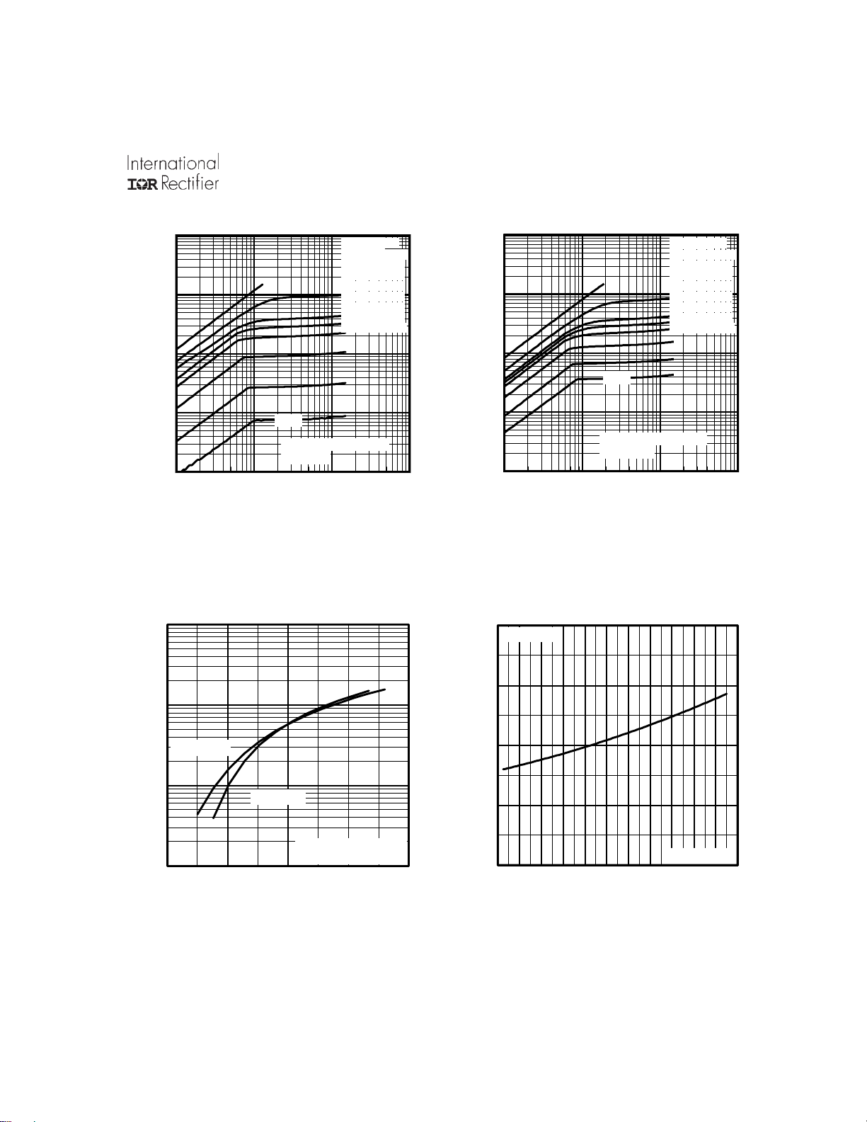
100
10
1
0.1
, Drain-to-Source Current (A)
D
-I
-2.5V
20µs PULSE WIDTH
Tj = 25°C
0.01
0.1 1 10 100
-VDS , Drain-to-Source Voltage (V)
100
VGS
TOP -10.0V
-4.5V
-3.7V
-3.5V
-3.3V
-3.0V
-2.7V
BOTTOM -2.5V
100
10
1
-2.5V
0.1
, Drain-to-Source Current (A)
D
-I
20µs PULSE WIDTH
Tj = 150°C
0.01
0.1 1 10 100
-VDS , Drain-to-Source Voltage (V)
Fig 2. Typical Output CharacteristicsFig 1. Typical Output Characteristics
2.0
-3.8A
I =
D
VGS
TOP -10.0V
-4.5V
-3.7V
-3.5V
-3.3V
-3.0V
-2.7V
BOTTOM -2.5V
1.5
10
T = 150 C
1
D
-I , Drain-to-Source Current (A)
0.1
2.0 3.0 4.0 5.0 6.0
°
J
°
T = 25 C
J
V = -15V
DS
20µs PULSE WIDTH
-V , Gate-to-Source Voltage (V)
GS
Fig 3. Typical Transfer Characteristics
1.0
(Normalized)
0.5
DS(on)
R , Drain-to-Source On Resistance
0.0
-60 -40 -20 0 20 40 60 80 100 120 140 160
T , Junction Temperature ( C)
J
Fig 4. Normalized On-Resistance
V =
GS
°
-10V
Vs. Temperature
www.irf.com 3
Page 4

IRF5805
800
600
400
C, Capacitance(pF)
200
0
1 10 100
V
= 0V, f = 1 MHZ
GS
C
= C
= C
= C
+ Cgd, C
gs
gd
ds
+ C
gd
iss
C
rss
C
oss
Ciss
Coss
Crss
VDS, Drain-to-Source Voltage (V)
Fig 5. Typical Capacitance Vs.
Drain-to-Source Voltage
100
SHORTED
ds
16
I =
-3.8A
D
12
8
4
GS
V =-24V
DS
V =-15V
DS
-V , Gate-to-Source Voltage (V)
0
0 2 4 6 8 10 12 14
Q , Total Gate Charge (nC)
G
Fig 6. Typical Gate Charge Vs.
Gate-to-Source Voltage
100
OPERATION IN THIS AREA LIMITED
BY R
DS(on)
10us
10
T = 150 C
1
SD
-I , Reverse Drain Current (A)
0.1
0.0 0.5 1.0 1.5 2.0 2.5 3.0
°
J
°
T = 25 C
J
V = 0 V
GS
-V ,Source-to-Drain Voltage (V)
SD
Fig 7. Typical Source-Drain Diode
10
1
D
-I , Drain Current (A)I , Drain Current (A)
°
= 25 C
C
T T= 150 C
Single Pulse
0.1
0.1 1 10 100
°
J
-V , Drain-to-Source Voltage (V)
DS
Fig 8. Maximum Safe Operating Area
100us
1ms
10ms
Forward Voltage
4 www.irf.com
Page 5

IRF5805
4.0
3.0
2.0
D
-I , Drain Current (A)
1.0
0.0
25 50 75 100 125 150
T , Case Temperature ( C)
C
°
Fig 9. Maximum Drain Current Vs.
Case Temperature
100
R
D.U.T.
D
-
+
V
V
DS
V
GS
R
G
V
GS
Pulse Width ≤ 1 µs
Duty Factor ≤ 0.1 %
Fig 10a. Switching Time Test Circuit
V
GS
10%
90%
V
DS
t
d(on)tr
t
d(off)tf
Fig 10b. Switching Time Waveforms
DD
D = 0.50
thJA
Thermal Response(Z )
0.20
10
0.10
0.05
0.02
0.01
1
0.1
0.00001 0.0001 0.001 0.01 0.1 1 10
SINGLE PULSE
(THERMAL RESPONSE)
Notes:
1. Duty factor D = t / t
2. Peak T = P x Z + T
t , Rectangular Pulse Duration (sec)
1
J DM thJA A
P
DM
t
1 2
1
t
2
Fig 11. Maximum Effective Transient Thermal Impedance, Junction-to-Ambient
www.irf.com 5
Page 6

IRF5805
0.500
)
0.450
0.400
0.350
0.300
0.250
0.200
0.150
, Drain-to -Source On Resistance (Ω
0.100
DS(on)
R
0.050
2.0 3.0 4.0 5.0 6.0 7.0 8.0 9.0 10.0
-V
Gate -to -Source Voltage (V)
GS,
ID = -3.8A
Fig 12. Typical On-Resistance Vs.
Gate Voltage
0.400
)
Ω
0.300
VGS = -4.5V
0.200
VGS = -10V
0.100
, Drain-to-Source On Resistance (
DS ( on )
R
0.000
0 5 10 15 20
-ID , Drain Current ( A )
Fig 13. Typical On-Resistance Vs.
Drain Current
Current Regulator
Same Type as D.U.T.
50KΩ
Q
G
Q
GS
V
G
Q
GD
Charge
Fig 14a. Basic Gate Charge Waveform
Fig 14b. Gate Charge Test Circuit
12V
.2µF
V
GS
.3µF
D.U.T .
-3mA
I
G
Current Sampling Resistors
V
DS
+
I
D
6 www.irf.com
Page 7

IRF5805
2.5
2.3
2.1
( V )
GS(th)
1.9
-V
1.7
1.5
-75 -50 -25 0 25 50 75 100 125 150
TJ , Temperature ( °C )
ID = -250µA
Fig 15. Typical Vgs(th) Vs.
Junction Temperature
30
25
20
15
Power (W)
10
5
0
0.001 0.010 0.100 1.000 10.000 100.000
Time (sec)
Fig 16. Typical Power Vs. Time
www.irf.com 7
Page 8

IRF5805
TSOP-6 Package Outline
TSOP-6 Part Marking Information
8 www.irf.com
Page 9

TSOP-6 Tape & Reel Information
IRF5805
IR EUROPEAN REGIONAL CENTRE: 439/445 Godstone Rd, Whyteleafe, Surrey CR3 OBL, UK Tel: ++ 44 (0)20 8645 8000
IR SOUTHEAST ASIA: 1 Kim Seng Promenade, Great World City West Tower, 13-11, Singapore 237994 Tel: ++ 65 (0)838 4630
IR WORLD HEADQUARTERS: 233 Kansas St., El Segundo, California 90245, USA Tel: (310) 252-7105
IR CANADA: 15 Lincoln Court, Brampton, Ontario L6T3Z2, Tel: (905) 453 2200
IR GERMANY: Saalburgstrasse 157, 61350 Bad Homburg Tel: ++ 49 (0) 6172 96590
IR ITALY: Via Liguria 49, 10071 Borgaro, Torino Tel: ++ 39 011 451 0111
IR JAPAN: K&H Bldg., 2F, 30-4 Nishi-Ikebukuro 3-Chome, Toshima-Ku, Tokyo 171 Tel: 81 (0)3 3983 0086
IR TAIWAN:16 Fl. Suite D. 207, Sec. 2, Tun Haw South Road, Taipei, 10673 Tel: 886-(0)2 2377 9936
Data and specifications subject to change without notice. 11/00
www.irf.com 9
 Loading...