

Page 1
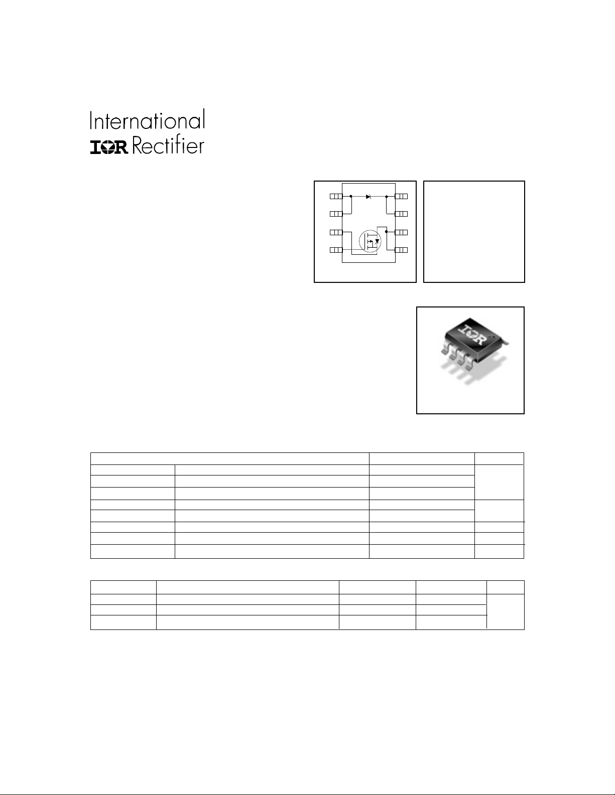
Co-packaged HEXFET Power
l
MOSFET and Schottky Diode
l Ideal For Buck Regulator Applications
l P-Channel HEXFET
l Low V
l SO-8 Footprint
Schottky Rectifier
F
Description
The FETKYTM family of Co-packaged HEXFETs and
Schottky diodes offer the designer an innovative board
space saving solution for switching regulator and
power management applications. HEXFETs utilize
advanced processing techniques to achieve extremely
low on-resistance per silicon area. Combining this
technology with International Rectifier's low forward
drop Schottky rectifiers results in an extremely efficient
device suitable for use in a wide variety of portable
electronics applications.
PD- 94016
IRF5803D2
FETKY MOSFET & Schottky Diode
A
A
S
G
TM
1
2
3
4
Top View
8
K
V
= -40V
R
DS(on)
DSS
= 112mΩ
7
K
6
D
5
D
Schottky Vf = 0.51V
The SO-8 has been modified through a customized
leadframe for enhanced thermal characteristics. The
SO-8
SO-8 package is designed for vapor phase, infrared or
wave soldering techniques.
Absolute Maximum Ratings (TA = 25°C Unless Otherwise Noted)
Parameter Maximum Units
ID @ TA = 25°C Continuous Drain Current, VGS @ -10V -3.4 A
ID @ TA = 70°C Continuous Drain Current, VGS @ -10V -2.7
I
DM
PD @TA = 25°C Power Dissipation 2.0 W
PD @TA = 70°C Power Dissipation 1.3
V
GS
T
J, TSTG
Pulsed Drain Current ➀ -27
Linear Derating Factor 16 mW/° C
Gate-to-Source Voltage ± 20 V
Junction and Storage Temperature Range -55 to +150 °C
Thermal Resistance
Symbol Parameter Typ. Max. Units
R
θJL
R
θJA
R
θJA
Notes:
Repetitive rating – pulse width limited by max. junction temperature (see fig. 11)
Pulse width ≤ 400µs – duty cycle ≤ 2%
Surface mounted on 1 inch square copper board, t ≤ 10sec.
Junction-to-Drain Lead, MOSFET ––– 20
Junction-to-Ambient , MOSFET ––– 62.5 °C/W
Junction-to-Ambient , SCHOTTKY ––– 62.5
www.irf.com 1
03/05/01
Page 2
IRF5803D2
Electrical Characteristics @ TJ = 25°C (unless otherwise specified)
Parameter Min. Typ. Max. Units Conditions
V
(BR)DSS
∆V
(BR)DSS
R
DS(on)
V
GS(th)
g
fs
I
DSS
I
GSS
Q
g
Q
gs
Q
gd
t
d(on)
t
r
t
d(off)
t
f
C
iss
C
oss
C
rss
MOSFET Source-Drain Ratings and Characteristics
I
S
I
SM
V
SD
t
rr
Q
rr
Schottky Diode Maximum Ratings
If (av) Max. Average Forward Current 3. 0 50% Duty Cycle. Rectangular Waveform, TA =30°C
I
SM
Schottky Diode Electrical Specifications
Vfm Max. Forward Voltage Drop 0.51 If = 5.0A, Tj = 25°C
Vrrm Max. Working Peak Reverse Voltage 40
Irm Max. Reverse Leakage Current 3.0 mA Vr = 40V Tj = 25°C
Ct Max. Junction Capacitance 405 pF Vr = 5Vdc ( 100kHz to 1 MHz) 25°C
Drain-to-Source Breakdown Voltage -40 ––– ––– VVGS = 0V, ID = -250µA
/∆T
Breakdown Voltage Temp. Coefficient ––– -0.03 ––– V/°C Reference to 25°C, ID = -1mA
J
Static Drain-to-Source On-Resistance
––– ––– 112 VGS = -10V, ID = -3.4A
––– ––– 190 V
mΩ
= -4.5V, ID = -2.7A
GS
Gate Threshold Voltage -1.0 ––– -3.0 V VDS = VGS, ID = -250µA
Forward Transconductance 4.0 ––– ––– SVDS = -10V, ID = -3.4A
Drain-to-Source Leakage Current
Gate-to-Source Forward Leakage ––– ––– -100 VGS = -20V
Gate-to-Source Reverse Leakage ––– ––– 100 VGS = 20V
––– ––– -10 VDS = -32V, VGS = 0V
––– ––– -25 VDS = -32V, VGS = 0V, TJ = 70°C
µA
nA
Total Gate Charge ––– 25 37 ID = -3.4A
Gate-to-Source Charge ––– 4.5 6.8 nC VDS = -20V
Gate-to-Drain ("Miller") Charge ––– 3.5 5.3 VGS = -10V, See Fig. 6 & 14
Turn-On Delay Time ––– 43 65 VDD = -20V
Rise Time ––– 550 825 ID = -1.0A
Turn-Off Delay Time ––– 88 130 RG = 6.0Ω
ns
Fall Time ––– 50 75 VGS = -10V,
Input Capacitance ––– 1110 ––– VGS = 0V
Output Capacitance ––– 93 ––– pF VDS = -25V
Reverse Transfer Capacitance ––– 73 ––– ƒ = 100kHz, See Fig. 5
Parameter Min. Typ. Max. Units Conditions
Continuous Source Current(Body Diode) ––– ––– -2.0
Pulsed Source Current (Body Diode) ––– ––– -27
A
Body Diode Forward Voltage ––– ––– -1.2 V TJ = 25°C, IS = -2.0A, VGS = 0V
Reverse Recovery Time (Body Diode) ––– 27 40 ns TJ = 25°C, IF = -2.0A
Reverse Recovery Charge ––– 34 50 nC di/dt = 100A/µs
Parameter Max. Units Conditions
A
See Fig.21
Max. peak one cycle Non-repetitive 34 0 5µs sine or 3µs Rect. pulse Following any rated
Surge current 70 10ms sine or 6ms Rect. pulse load condition &
A
with Vrrm applied
Parameter Max. Units Conditions
0.63 If = 10A, Tj = 25°C
V
0.44 If = 5.0A, Tj = 125°C
0.59 If = 10A, Tj = 125°C
V
37 Tj = 125°C
2 www.irf.com
Page 3
Power Mosfet Characteristics
IRF5803D2
100
10
1
0.1
, Drain-to-Source Current (A)
D
-I
20µs PULSE WIDTH
Tj = 25°C
-2.7V
0.01
0.1 1 10 100
-VDS, Drain-to-Source Voltage (V)
100
°
T = 25 C
J
VGS
TOP -15V
-10V
-4.5V
-3.7V
-3.5V
-3.3V
-3.0V
BOTTOM - 2.7V
100
10
1
-2.7V
0.1
, Drain-to-Source Current (A)
D
-I
20µs PULSE WIDTH
Tj = 125°C
0.01
0.1 1 10 100
-VDS, Drain-to-Source Voltage (V)
Fig 2. Typical Output CharacteristicsFig 1. Typical Output Characteristics
2.0
-3.4A
I =
D
VGS
TOP -15V
-10V
-4.5V
-3.7V
-3.5V
-3.3V
-3.0V
BOTTOM - 2.7V
1.5
10
T = 150 C
1
D
-I , Drain-to-Source Current (A)
V = -25V
DS
0.1
2.0 3.0 4.0 5.0 6.0 7.0 8.0
-V , Gate-to-Source Voltage (V)
GS
20µs PULSE WIDTH
Fig 3. Typical Transfer Characteristics
°
J
1.0
(Normalized)
0.5
DS(on)
R , Drain-to-Source On Resistance
0.0
-60 -40 -20 0 20 40 60 80 100 120 140 160
T , Junction Temperature ( C)
J
V =
GS
°
-
-10V
Fig 4. Normalized On-Resistance
Vs. Temperature
www.irf.com 3
Page 4
IRF5803D2
Power Mosfet Characteristics
2000
1500
Ciss
1000
C, Capacitance(pF)
500
Coss
Crss
0
1 10 100
-
V
= 0V, f = 100 KHZ
GS
C
= C
iss
SHORTED
C
= C
rss
C
= C
oss
VDS, Drain-to-Source Voltage (V)
gd
ds
+ C
gs
gd
+ Cgd, C
Fig 5. Typical Capacitance Vs.
Drain-to-Source Voltage
100
ds
12
I =
-3.4A
D
10
8
6
4
GS
2
-V , Gate-to-Source Voltage (V)
0
0 5 10 15 20 25 30
Q , Total Gate Charge (nC)
G
V =-32V
DS
V =-20V
DS
Fig 6. Typical Gate Charge Vs.
Gate-to-Source Voltage
100
OPERATION IN THIS AREA
LIMITED BY RDS(on)
T = 150 C
10
1
SD
-I , Reverse Drain Current (A)
0.1
0.4 0.8 1.2 1.6
-V ,Source-to-Drain Voltage (V)
SD
Fig 7. Typical Source-Drain Diode
°
J
10
°
T = 25 C
J
100µsec
1
1msec
10msec
V = 0 V
GS
, Drain-to-Source Current (A)
D
-I
TA = 25°C
TJ = 150°C
Single Pulse
0.1
1 10 100
-V
, Drain-toSource Voltage (V)
DS
Fig 8. Maximum Safe Operating Area
Forward Voltage
4 www.irf.com
Page 5

Power Mosfet Characteristics
(
)
IRF5803D2
3.5
3.0
2.5
2.0
1.5
D
1.0
-I , Drain Current (A)
0.5
0.0
25 50 75 100 125 150
T , Case Temperature ( C)
C
°
Fig 9. Maximum Drain Current Vs.
Case Temperature
100
R
D.U.T.
D
-
+
V
V
DS
V
GS
R
G
V
GS
Pulse Width ≤ 1 µs
Duty Factor ≤ 0.1 %
Fig 10a. Switching Time Test Circuit
V
GS
10%
90%
V
DS
t
d(on)tr
t
d(off)tf
Fig 10b. Switching Time Waveforms
DD
D = 0.50
thJA
0.20
10
0.10
0.05
0.02
0.01
1
SINGLE PULSE
THERMAL RESPONSE
Thermal Response (Z )
Notes:
1. Duty factor D = t / t
2. Peak T =P x Z + T
0.1
0.00001 0.0001 0.001 0.01 0.1 1 10 100
t , Rectangular Pulse Duration (sec)
1
J DM thJA A
P
DM
t
1
1 2
t
2
Fig 11. Maximum Effective Transient Thermal Impedance, Junction-to-Ambient
www.irf.com 5
Page 6

IRF5803D2
0.20
)
Ω
0.15
Power Mosfet Characteristics
0.40
)
Ω
0.30
VGS = -4.5V
0.10
0.05
, Drain-to -Source On Resistance (
DS(on)
R
0.00
4.0 8.0 12.0 16.0
-V
GS,
ID = -3.4A
Gate -to -Source Voltage (V)
Fig 12. Typical On-Resistance Vs.
Gate Voltage
Q
G
Q
GS
Q
GD
0.20
0.10
, Drain-to-Source On Resistance (
DS ( on )
R
0.00
VGS = -10V
0.0 5.0 10.0 15.0
-ID , Drain Current ( A )
Fig 13. Typical On-Resistance Vs.
Drain Current
Current Regulator
Same Type as D.U.T.
50KΩ
.2µF
12V
.3µF
D.U.T.
V
DS
+
V
V
G
Charge
Fig 14a. Basic Gate Charge Waveform
GS
-3mA
I
G
Current Sampling Resistors
I
D
Fig 14b. Gate Charge Test Circuit
6 www.irf.com
Page 7

Power Mosfet Characteristics
30
IRF5803D2
2.8
ID = -250µA
2.4
( V )
GS(th)
-V
2.0
1.6
-75 -50 -25 0 25 50 75 100 125 150
TJ , Temperature ( °C )
Fig 15. Typical Vgs(th) Vs.
Junction Temperature
25
20
15
Power (W)
10
5
0
0.001 0.010 0.100 1.000 10.000 100.000
Time (sec)
Fig 16. Typical Power Vs. Time
www.irf.com 7
Page 8

IRF5803D2
Schottky Diode Characteristics
100
F
T = 150°C
J
T = 125°C
J
10
T = 25 ° C
J
Reverse Curre nt - I ( m A)
100
T = 15 0°C
J
10
R
1
0.1
0.01
0.001
125°C
100°C
75°C
50°C
25°C
0 5 10 15 20 25 30 35 40
Reverse Voltag e - V (V)
R
Fig. 18 - Typical Values of
Reverse Current Vs. Reverse Voltage
T
1000
T = 25°C
J
Instantan e o u s F or w ard Cu rrent - I (A)
1
0 0.2 0.4 0.6 0.8 1 1.2 1.4 1.6 1.8 2 2.2
Fo rw ard Vo lt a ge Dr o p - V (V)
Fig. 17 - Maximum Forward Voltage Drop
Characteristics
FM
Junction Cap a c ita nce - C (p F )
100
0 5 10 15 20 25 30 35 40 45
Reverse Voltage - V (V)
R
Fig. 19 - Typical Junction Capacitance
Vs. Reverse Voltage
8 www.irf.com
Page 9

IRF5803D2
Schottky Diode Characteristics
100
D = 0.50
0.20
10
thJA
0.10
0.05
0.02
1
0.01
P
DM
t
SINGLE PULSE
0.1
Thermal Response (Z )
0.01
0.00001 0.0001 0.001 0.01 0.1 1 10 100
(THERMAL RESPONSE)
Notes:
1. Duty factor D =t / t
2. Peak T =P x Z + T
t , Rectangular Pulse Duration (sec)
1
J DM thJA A
Fig 20. Maximum Effective Transient Thermal Impedance, Junction-to-Ambient
180
1
1 2
t
2
160
°C)
R
140
120
100
80
60
see note (4)
40
Allowable Ambient Temprature - (
quare wave ( D = 0.50)
S
20
80 % Rated VR applied
0
0 1 2 3 4 5 6
DC
Average Forward Current - I
thJA
F(AV)
= 62.5 °C/W
(A)
Fig.21 - Maximum Allowable Ambient
Temp. Vs. Forward Current
Note (4) Formula used: TC = TJ - (Pd + Pd
Pd = Forward Power Loss = I
Pd
= Inverse Power Loss = VR1 x IR (1 - D); IR @ V
REV
F(AV)
x VFM @ (I
REV
) x R
F(AV)
thJA
/ D) ;
;
R1
= 80% rated V
R
www.irf.com 9
Page 10

IRF5803D2
SO-8 Package Details
D B
8X b
5
65
4312
e1
A1
H
0.25 [.010]
A
A
C
0.10 [.004]
A
87
6
E
e
6X
0.25 [.010] C A B
NOTES:
1. DIMENSIONING & T OLERANCING PER AS ME Y14.5M-1994.
2. CONTROLLING DIMENSION: MILLIMETER
3. DIMENSIONS ARE SHOWN IN MILLIMETERS [INCHES].
4. OUT LINE CONF ORMS T O JE DE C OUT LINE MS -012AA.
5 DIMENSION DOES NOT INCLUDE MOLD PROTRUSIONS.
MOLD PROTRUSIONS NOT TO EXCEED 0.15 [.006].
6 DIMENSION DOES NOT INCLUDE MOLD PROTRUSIONS.
MOLD PROTRUSIONS NOT TO EXCEED 0.25 [.010].
7 DIMENSION IS THE LENGTH OF LEAD FOR SOLDERING TO
A SUBSTRATE.
y
3X 1.27 [.05 0]
DIM
MIN MAX
A
.0532
A1
b
c .0075 .0098 0.19 0.25
D
E
e
e1
H
K
L
y
K x 45°
8X L
7
6.46 [.255]
.0688
.0040
.0098
.013
.020
.189
.1968
.1497
.1574
.050 BASIC
.025 BASIC 0.635 BAS IC
.2284
.2440
.0099
.0196
.016
.050
0°
8°
8X c
FOOT PRINT
8X 0.72 [.02 8]
MILLIMET ERSINCH ES
MIN MAX
1.35
1.75
0.10
0.25
0.33
0.51
4.80
5.00
3.80
4.00
1.27 BASIC
5.80
6.20
0.25
0.50
0.40
1.27
0°
8°
8X 1.78 [.07 0]
SO-8 Part Marking
EXAMPLE: THIS IS AN IRF7101 (MOSFET)
DATE CODE (YWW)
Y = LAST DIGIT OF THE YEAR
YW W
XXXX
INTERNATIONAL
F7101
RECT IFIER
LOGO
10 www.irf.com
WW = WEEK
LOT CODE
PART NUMBER
Page 11

(
)
)
)
)
)
)
)
SO-8 Tape and Reel
TE R MIN AL N U M BER 1
12.3 ( .484
11.7 ( .461
IRF5803D2
8.1 ( .318
7.9 ( .312
NOTES:
1. CONTROLLING DIMENSION : MILLIMETER.
2. ALL DIM ENSIONS ARE SHOWN IN MILLIM ETERS(INCHES).
3. OUT LINE CO N F O RMS TO EIA-481 & E IA-541.
330.00
12.992
MAX.
NOTES :
1. CONTRO LLING DIMEN SION : MILLIMETER.
2. OU TL INE CO NF O R M S TO EIA-481 & EIA-541.
FEED DIRECTION
Data and specifications subject to change without notice.
This product has been designed and qualified for the consumer market.
Qualification Standards can be found on IR’s Web site.
14.40 ( .566
12.40 ( .488
IR WORLD HEADQUARTERS: 233 Kansas St., El Segundo, California 90245, USA Tel: (310) 252-7105
TAC Fax: (310) 252-7903
Visit us at www.irf.com for sales contact information.03/01
www.irf.com 11
 Loading...