

Page 1
Parameter Max. Units
V
DS
Drain- Source Voltage -40 V
ID @ TA = 25°C Continuous Drain Current, VGS @ -10V -3.4
ID @ TA= 70°C Continuous Drain Current, VGS @ -10V -2.7 A
I
DM
Pulsed Drain Current -27
PD @TA = 25°C Power Dissipation 2.0
PD @TA = 70°C Power Dissipation 1.3
Linear Derating Factor 16 mW/°C
V
GS
Gate-to-Source Voltage ± 20 V
T
J, TSTG
Junction and Storage Temperature Range -55 to + 150 °C
03/05/01
www.irf.com 1
IRF5803
HEXFET® Power MOSFET
Parameter Max. Units
R
θJA
Maximum Junction-to-Ambient 62.5 °C/W
Thermal Resistance
Absolute Maximum Ratings
W
V
DSS
R
DS(on)
max (m
Ω)Ω)
Ω)Ω)
Ω) I
D
-40V 112@VGS = -10V -3.4A
190@VGS = -4.5V -2.7A
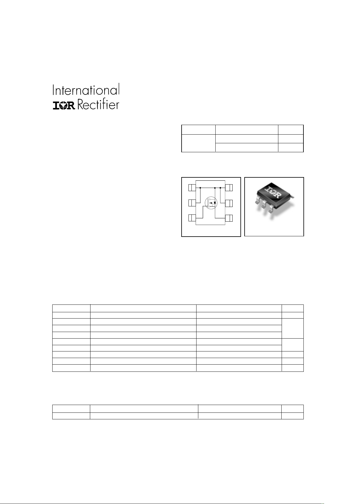
TSOP-6
These P-channel HEXFET® Power MOSFETs from
International Rectifier utilize advanced processing
techniques to achieve the extremely low on-resistance
per silicon area. This benefit provides the designer
with an extremely efficient device for use in battery and
load management applications.
The TSOP-6 package with its customized leadframe
produces a HEXFET
®
power MOSFET with R
DS(on)
60% less than a similar size SOT-23. This package is
ideal for applications where printed circuit board space
is at a premium. It's unique thermal design and R
DS(on)
reduction enables a current-handling increase of nearly
300% compared to the SOT-23.
Description
l Ultra Low On-Resistance
l P-Channel MOSFET
l Surface Mount
l Available in Tape & Reel
l Low Gate Charge
Top View
1
2
D
G
A
D
D
D
S
3
4
5
6
PD-94015
Page 2
IRF5803
2 www.irf.com
Parameter Min. Typ. Max. Units Conditions
V
(BR)DSS
Drain-to-Source Breakdown Voltage -40 ––– ––– VVGS = 0V, ID = -250µA
∆V
(BR)DSS
/∆T
J
Breakdown Voltage Temp. Coefficient ––– 0.03 ––– V/°C Reference to 25°C, ID = -1mA
––– ––– 112 VGS = -10V, ID = -3.4
––– ––– 190 V
GS
= -4.5V, ID = -2.7A
V
GS(th)
Gate Threshold Voltage -1.0 ––– -3.0 V VDS = VGS, ID = -250µA
g
fs
Forward Transconductance 4.0 ––– ––– SVDS = -10V, ID = -3.4A
––– ––– -10 VDS = -32V, VGS = 0V
––– ––– -25 VDS = -32V, VGS = 0V, TJ = 70°C
Gate-to-Source Forward Leakage ––– ––– -100 VGS = -20V
Gate-to-Source Reverse Leakage ––– ––– 100 VGS = 20V
Q
g
Total Gate Charge ––– 25 37 ID = -3.4A
Q
gs
Gate-to-Source Charge ––– 4.5 6.8 nC VDS = -20V
Q
gd
Gate-to-Drain ("Miller") Charge ––– 3.5 5.3 VGS = -10V
t
d(on)
Turn-On Delay Time ––– 43 ––– VDD = -20V
t
r
Rise Time ––– 550 ––– ID = -1.0A
t
d(off)
Turn-Off Delay Time ––– 88 ––– RG = 6.0Ω
t
f
Fall Time ––– 50 ––– VGS = -10V
C
iss
Input Capacitance ––– 1110 ––– VGS = 0V
C
oss
Output Capacitance ––– 93 ––– pF VDS = -25V
C
rss
Reverse Transfer Capacitance ––– 73 ––– ƒ = 100kHz
Parameter Min. Typ. Max. Units Conditions
I
S
Continuous Source Current MOSFET symbol
(Body Diode) showing the
I
SM
Pulsed Source Current integral reverse
(Body Diode) p-n junction diode.
V
SD
Diode Forward Voltage ––– ––– -1.2 V TJ = 25°C, IS = -2.0A, VGS = 0V
t
rr
Reverse Recovery Time ––– 27 40 ns TJ = 25°C, IF = -2.0A
Q
rr
Reverse Recovery Charge ––– 34 50 nC di/dt = -100A/µs
Source-Drain Ratings and Characteristics
A
-27
–––
–––
–––
-2.0
–––
S
D
G
Repetitive rating; pulse width limited by
max. junction temperature.
Notes:
Pulse width ≤ 400µs; duty cycle ≤ 2%.
Electrical Characteristics @ TJ = 25°C (unless otherwise specified)
I
GSS
µA
mΩ
R
DS(on)
Static Drain-to-Source On-Resistance
I
DSS
Drain-to-Source Leakage Current
nA
ns
Surface mounted on 1 in square Cu board
Page 3
IRF5803
www.irf.com 3
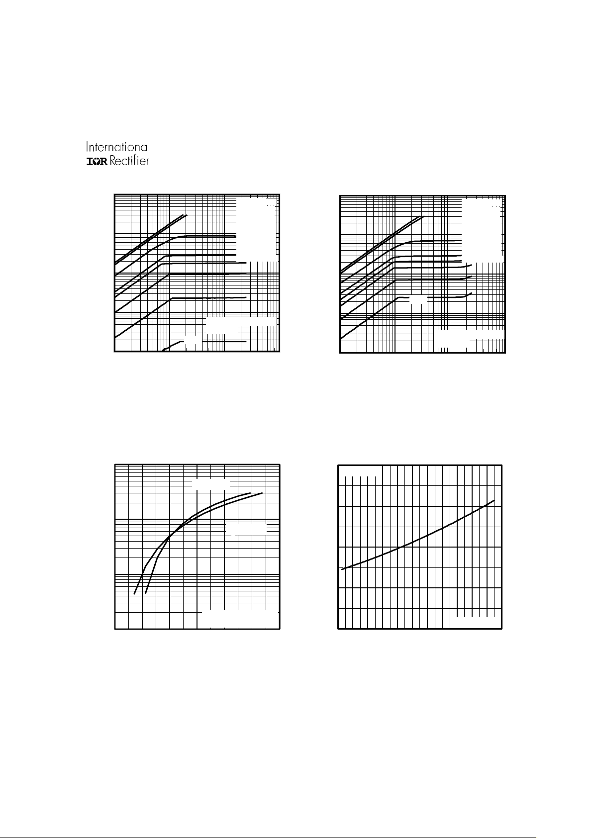
Fig 4. Normalized On-Resistance
Vs. Temperature
Fig 2. Typical Output CharacteristicsFig 1. Typical Output Characteristics
Fig 3. Typical Transfer Characteristics
-
0.1
1
10
100
2.0 3.0 4.0 5.0 6.0 7.0 8.0
V = -25V
20µs PULSE WIDTH
DS
-V , Gate-to-Source Voltage (V)
-I , Drain-to-Source Current (A)
GS
D
T = 25 C
J
°
T = 150 C
J
°
-60 -40 -20 0 20 40 60 80 100 120 140 160
0.0
0.5
1.0
1.5
2.0
T , Junction Temperature ( C)
R , Drain-to-Source On Resistance
(Normalized)
J
DS(on)
°
V =
I =
GS
D
-10V
-3.4A
0.1 1 10 100
-VDS, Drain-to-Source Voltage (V)
0.01
0.1
1
10
100
-I
D
, Drain-to-Source Current (A)
-2.7V
20µs PULSE WIDTH
Tj = 25°C
VGS
TOP -15V
-10V
-4.5V
-3.7V
-3.5V
-3.3V
-3.0V
BOTTOM - 2.7V
0.1 1 10 100
-VDS, Drain-to-Source Voltage (V)
0.01
0.1
1
10
100
-I
D
, Drain-to-Source Current (A)
-2.7V
20µs PULSE WIDTH
Tj = 125°C
VGS
TOP -15V
-10V
-4.5V
-3.7V
-3.5V
-3.3V
-3.0V
BOTTOM - 2.7V
Page 4

IRF5803
4 www.irf.com
Fig 8. Maximum Safe Operating Area
Fig 6. Typical Gate Charge Vs.
Gate-to-Source Voltage
Fig 5. Typical Capacitance Vs.
Drain-to-Source Voltage
Fig 7. Typical Source-Drain Diode
Forward Voltage
-
1 10 100
VDS, Drain-to-Source Voltage (V)
0
500
1000
1500
2000
C, Capacitance(pF)
Coss
Crss
Ciss
V
GS
= 0V, f = 100 KHZ
C
iss
= C
gs
+ Cgd, C
ds
SHORTED
C
rss
= C
gd
C
oss
= C
ds
+ C
gd
0 5 10 15 20 25 30
0
2
4
6
8
10
12
Q , Total Gate Charge (nC)
-V , Gate-to-Source Voltage (V)
G
GS
I =
D
-3.4A
V =-20V
DS
V =-32V
DS
0.1
1
10
100
0.4 0.8 1.2 1.6
-V ,Source-to-Drain Voltage (V)
-I , Reverse Drain Current (A)
SD
SD
V = 0 V
GS
T = 25 C
J
°
T = 150 C
J
°
1 10 100
-V
DS
, Drain-toSource Voltage (V)
0.1
1
10
100
-I
D
, Drain-to-Source Current (A)
TA = 25°C
TJ = 150°C
Single Pulse
1msec
10msec
OPERATION IN THIS AREA
LIMITED BY RDS(on)
100µsec
Page 5

IRF5803
www.irf.com 5
Fig 11. Maximum Effective Transient Thermal Impedance, Junction-to-Ambient
Fig 9. Maximum Drain Current Vs.
Case Temperature
V
DS
V
GS
Pulse Width ≤ 1 µs
Duty Factor ≤ 0.1 %
R
D
V
GS
V
DD
R
G
D.U.T.
+
-
V
DS
90%
10%
V
GS
t
d(on)tr
t
d(off)tf
Fig 10a. Switching Time Test Circuit
Fig 10b. Switching Time Waveforms
25 50 75 100 125 150
0.0
0.5
1.0
1.5
2.0
2.5
3.0
3.5
T , Case Temperature ( C)
-I , Drain Current (A)
°
C
D
0.1
1
10
100
0.00001 0.0001 0.001 0.01 0.1 1 10 100
Notes:
1. Duty factor D = t / t
2. Peak T =P x Z + T
1 2
J DM thJA A
P
t
t
DM
1
2
t , Rectangular Pulse Duration (sec)
Thermal Response (Z )
1
thJA
0.01
0.02
0.05
0.10
0.20
D = 0.50
SINGLE PULSE
(
THERMAL RESPONSE
)
Page 6

IRF5803
6 www.irf.com
Fig 13. Typical On-Resistance Vs.
Drain Current
Fig 12. Typical On-Resistance Vs.
Gate Voltage
Fig 14b. Gate Charge Test Circuit
Fig 14a. Basic Gate Charge Waveform
Q
G
Q
GS
Q
GD
V
G
Charge
D.U.T .
V
DS
I
D
I
G
-3mA
V
GS
.3µF
50KΩ
.2µF
12V
Current Regulator
Same Type as D.U.T.
Current Sampling Resistors
+
-
0.0 5.0 10.0 15.0
-ID , Drain Current ( A )
0.00
0.10
0.20
0.30
0.40
R
DS ( on )
, Drain-to-Source On Resistance (
Ω
)
VGS = -4.5V
VGS = -10V
4.0 8.0 12.0 16.0
-V
GS,
Gate -to -Source Voltage (V)
0.00
0.05
0.10
0.15
0.20
R
DS(on)
, Drain-to -Source On Resistance (
Ω
)
ID = -3.4A
Page 7

IRF5803
www.irf.com 7
Fig 16. Typical Power Vs. Time
Fig 15. Typical Threshold Voltage Vs.
Junction Temperature
-75 -50 -25 0 25 50 75 100 125 150
TJ , Temperature ( °C )
1.6
2.0
2.4
2.8
-V
GS(th)
( V )
ID = -250µA
0.001 0.010 0.100 1.000 10.000 100.000
Time (sec)
0
5
10
15
20
25
30
Power (W)
Page 8

IRF5803
8 www.irf.com
TSOP-6 Package Outline
TSOP-6 Part Marking Information
WW = (1-26) IF PRE CEDED BY LAS T DIGIT OF CALENDAR YEAR
01
02
03
04
24
WYEAR Y
A2001 1
B2002 2
C2003 3
D2004 4
X
1999
0
W W = (2 7-52) IF PRECED ED BY A LETTER
WEEK
27
28
29
30
50
WYEAR
A2001 A
B2002 B
C2003 C
D2004 D
X
J
YWW = 9632 = FF
YWW = 9603 = 6C
DATE C ODE EXAMPLES:
2005
1996
1997
1998
1999
2000
E
F
G
H
K
Y
2005
1996
1997
1998
2000
9
8
7
6
5
PART NUMBER
EXAMPLE: THIS IS AN SI3443DV
YW
TOP
DATE
CODE
WORK
WEEK
WORK
3A = SI3443DV
PART NUM B ER CODE REFER ENCE:
25 Y
51 Y
26 Z
WAFE R LOT
BOTTOM
NUMBER CODE
3A
XXXX
3B = IRF5800
3C = IRF5850
3D = IRF5851
3E = IRF5852
3J = IRF5806
3I = IRF5805
Page 9

IRF5803
www.irf.com 9
TSOP-6 Tape & Reel Information
Data and specifications subject to change without notice.
This product has been designed and qualified for the consumer market.
Qualification Standards can be found on IR’s Web site.
IR WORLD HEADQUARTERS: 233 Kansas St., El Segundo, California 90245, USA Tel: (310) 252-7105
TAC Fax: (310) 252-7903
Visit us at www.irf.com for sales contact information.03/01
 Loading...