

Page 1
PD - 93936A
IRF3706
IRF3706SSMPS MOSFET
IRF3706L
HEXFET® Power MOSFET
Applications
l High Frequency Isolated DC-DC
Converters with Synchronous Rectification
V
DSS
20V 8.5mΩ 77A
for Telecom and Industrial Use
l High Frequency Buck Converters for
Computer Processor Power
Benefits
l Ultra-Low Gate Impedance
l Very Low R
l Fully Characterized Avalanche Voltage
and Current
DS(on)
at 4.5V V
GS
TO-220AB
IRF3706
Absolute Maximum Ratings
Symbol Parameter Max. Units
V
DS
V
GS
ID @ TC = 25°C Continuous Drain Current, VGS @ 10V 77
ID @ TC = 100°C Continuous Drain Current, VGS @ 10V 54 A
I
DM
PD @TC = 25°C Maximum Power Dissipation 88 W
PD @TC = 100°C Maximum Power Dissipation 44 W
Linear Derating Factor 0.59 W/°C
TJ , T
STG
Drain-Source Voltage 20 V
Gate-to-Source Voltage ± 12 V
Pulsed Drain Current 280
Junction and Storage Temperature Range -55 to + 175 °C
R
DS(on)
D2Pak
IRF3706S
max I
TO-262
IRF3706L
D
Thermal Resistance
Parameter Typ. Max. Units
R
θJC
R
θCS
R
θJA
R
θJA
Junction-to-Case ––– 1.7
Case-to-Sink, Flat, Greased Surface 0.50 ––– °C/W
Junction-to-Ambient ––– 62
Junction-to-Ambient (PCB mount) ––– 40
Notes through are on page 11
www.irf.com 1
7/5/00
Page 2
IRF3706/3706S/3706L
Static @ TJ = 25°C (unless otherwise specified)
Parameter Min. Typ. Max.Units Conditions
V
(BR)DSS
∆V
(BR)DSS
R
DS(on)
V
GS(th)
I
DSS
I
GSS
Dynamic @ TJ = 25°C (unless otherwise specified)
Symbol Parameter Min. Typ. Max. Units Conditions
g
fs
Q
g
Q
gs
Q
gd
Q
oss
t
d(on)
t
r
t
d(off)
t
f
C
iss
C
oss
C
rss
Drain-to-Source Breakdown Voltage 20 ––– ––– V VGS = 0V, ID = 250µA
/∆T
Breakdown Voltage Temp. Coefficient
J
––– 0.021 ––– V/°C Reference to 25°C, ID = 1mA
––– 6.0 8.5 VGS = 10V, ID = 36A
Static Drain-to-Source On-Resistance
––– 7.3 10.5 mΩ VGS = 4.5V, ID = 28A
––– 11 22 VGS = 2.8V, ID = 18A
Gate Threshold Voltage 0.6 ––– 2.0 V VDS = VGS, ID = 250µA
Drain-to-Source Leakage Current
––– ––– 20
––– ––– 100 VDS = 16V, VGS = 0V, TJ = 125°C
Gate-to-Source Forward Leakage ––– ––– 200 VGS = 12V
Gate-to-Source Reverse Leakage ––– ––– -200
VDS = 16V, VGS = 0V
µA
nA
VGS = -12V
Forward Transconductance 53 ––– ––– S VDS = 16V, ID = 57A
Total Gate Charge ––– 23 35 ID = 28A
Gate-to-Source Charge ––– 8.0 12 nC VDS = 10V
Gate-to-Drain ("Miller") Charge ––– 5.5 8.3 VGS = 4.5V
Output Gate Charge ––– 16 24 VGS = 0V, VDS = 10V
Turn-On Delay Time ––– 6.8 ––– VDD = 10V
Rise Time ––– 87 ––– ID = 28A
Turn-Off Delay Time ––– 17 –– – RG = 1.8Ω
ns
Fall Time ––– 4.8 ––– VGS = 4.5V
Input Capacitance ––– 2410 ––– VGS = 0V
Output Capacitance ––– 1070 ––– VDS = 10V
Reverse Transfer Capacitance ––– 140 ––– pF ƒ = 1.0MHz
Avalanche Characteristics
Symbol Parameter Typ. Max. Units
E
AS
I
AR
Single Pulse Avalanche Energy ––– 220 mJ
Avalanche Current ––– 28 A
Diode Characteristics
Symbol Parameter Min. Typ. Max. Units Conditions
I
S
I
SM
V
SD
t
rr
Q
rr
t
rr
Q
rr
Continuous Source Current MOSFET symbol
(Body Diode)
Pulsed Source Current integral reverse
(Body Diode)
Diode Forward Voltage
––– –––
––– –––
––– 0.88 1.3 V TJ = 25°C, IS = 36A, VGS = 0V
––– 0.82 ––– TJ = 125°C, IS = 36A, VGS = 0V
77
280
showing the
A
p-n junction diode.
G
Reverse Recovery Time ––– 45 68 ns TJ = 25°C, IF = 36A, VR=20V
Reverse Recovery Charge ––– 65 98 nC di/dt = 100A/µs
Reverse Recovery Time ––– 49 74 ns TJ = 125°C, IF = 36A, VR=20V
Reverse Recovery Charge ––– 78 120 nC di/dt = 100A/µs
2 www.irf.com
D
S
Page 3
IRF3706/3706S/3706L
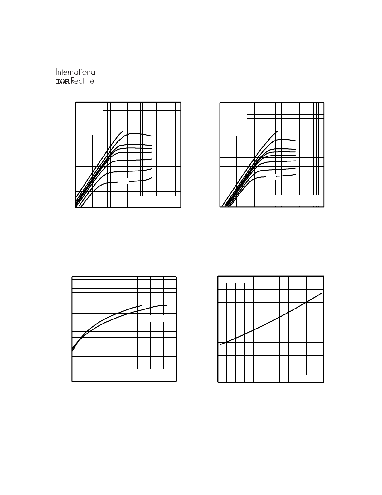
1000
100
D
I , Drain-to-Source Current (A)
10
0.1 1 10 100
1000
VGS
TOP
10V
4.5V
3.7V
3.5V
3.3V
3.0V
2.7V
BOTTOM
2.5V
2.5V
20µs PULSE WIDTH
T = 25 C
J
V , Drain-to-Source Voltage (V)
DS
°
1000
100
D
I , Drain-to-Source Current (A)
10
0.1 1 10 100
VGS
TOP
10V
4.5V
3.7V
3.5V
3.3V
3.0V
2.7V
BOTTOM
2.5V
2.5V
20µs PULSE WIDTH
T = 175 C
V , Drain-to-Source Voltage (V)
DS
°
J
Fig 2. Typical Output CharacteristicsFig 1. Typical Output Characteristics
2.0
71A
I =
D
°
T = 25 C
J
T = 175 C
J
100
D
I , Drain-to-Source Current (A)
V = 15V
DS
10
2.5 3.5 4.5 5.5 6.5
V , Gate-to-Source Voltage (V)
GS
20µs PULSE WIDTH
Fig 3. Typical Transfer Characteristics
°
1.5
1.0
(Normalized)
0.5
DS(on)
R , Drain-to-Source On Resistance
0.0
-60 -40 -20 0 20 40 60 80 100 120 140 160 180
T , Junction Temperature ( C)
J
Fig 4. Normalized On-Resistance
V =
10V
GS
°
Vs. Temperature
www.irf.com 3
Page 4
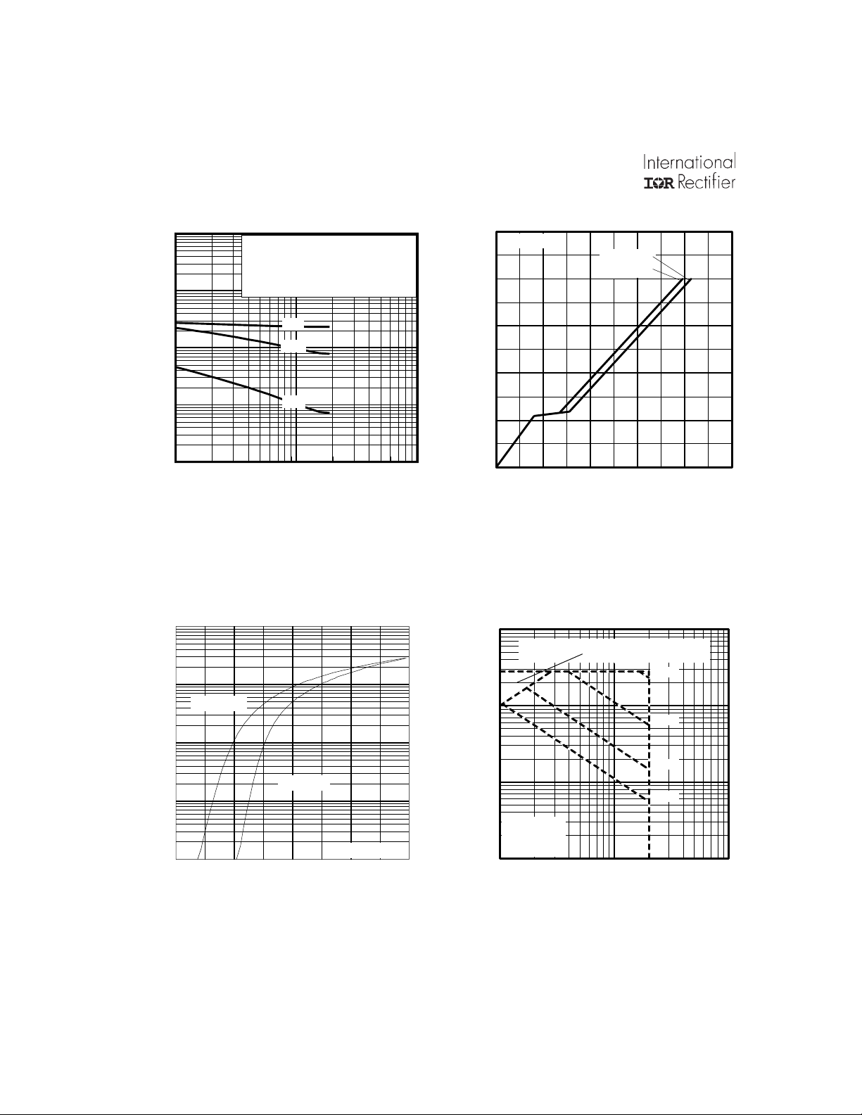
IRF3706/3706S/3706L
100000
10000
1000
C, Capacitance(pF)
100
10
1 10 100
V
= 0V, f = 1 MHZ
GS
C
= C
= C
= C
Coss
gs
gd
ds
Ciss
Crss
+ Cgd, C
+ C
gd
iss
C
rss
C
oss
VDS, Drain-to-Source Voltage (V)
Fig 5. Typical Capacitance Vs.
Drain-to-Source Voltage
1000
100
°
T = 175 C
J
SHORTED
ds
10
I =
28A
D
V = 16V
DS
V = 10V
8
6
4
2
GS
V , Gate-to-Source Voltage (V)
0
0 10 20 30 40 50
Q , Total Gate Charge (nC)
G
DS
Fig 6. Typical Gate Charge Vs.
Gate-to-Source Voltage
1000
100
OPERATION IN THIS AREA LIMITED
BY R
DS(on)
10us
100us
10
1ms
°
T = 25 C
J
1
SD
I , Reverse Drain Current (A)
V = 0 V
0.1
0.2 0.6 1.0 1.4 1.8
V ,Source-to-Drain Voltage (V)
SD
GS
Fig 7. Typical Source-Drain Diode
10
D
I , Drain Current (A)I , Drain Current (A)
°
= 25 C
C
T T= 175 C
Single Pulse
1
1 10 100
°
J
V , Drain-to-Source Voltage (V)
DS
10ms
Fig 8. Maximum Safe Operating Area
Forward Voltage
4 www.irf.com
Page 5

IRF3706/3706S/3706L
R
D.U.T.
D
+
V
DD
-
80
60
40
V
DS
V
GS
R
G
4.5V
Pulse Width ≤ 1 µs
Duty Factor ≤ 0.1 %
D
I , Drain Current (A)
20
0
25 50 75 100 125 150 175
T , Case Temperature ( C)
C
°
Fig 9. Maximum Drain Current Vs.
Fig 10a. Switching Time Test Circuit
V
DS
90%
10%
V
GS
t
d(on)tr
t
d(off)tf
Case Temperature
Fig 10b. Switching Time Waveforms
10
thJC
1
D = 0.50
0.20
0.10
0.05
0.1
0.02
0.01
SINGLE PULSE
(THERMAL RESPONSE)
Thermal Response (Z )
Notes:
1. Duty factor D = t / t
2. Peak T =P x Z + T
0.01
0.00001 0.0001 0.001 0.01 0.1
t , Rectangular Pulse Duration (sec)
1
J DM thJC C
P
DM
t
1 2
1
t
2
Fig 11. Maximum Effective Transient Thermal Impedance, Junction-to-Case
www.irf.com 5
Page 6

IRF3706/3706S/3706L
A
15V
DRIVER
+
-
V
R
20V
V
DS
G
t
L
D.U.T
I
AS
0.01
p
Ω
Fig 12a. Unclamped Inductive Test Circuit
V
(B R)DSS
t
p
I
AS
Fig 12b. Unclamped Inductive Waveforms
DD
500
TOP
400
300
200
100
AS
E , Single Pulse Avalanche Energy (mJ)
0
25 50 75 100 125 150 175
Starting T , Junction Temperature ( C)
J
BOTTOM
Fig 12c. Maximum Avalanche Energy
Vs. Drain Current
I
°
D
12A
24A
28A
Current Regulator
Same Type as D.U.T.
Q
G
4.5 V
Q
GS
V
G
Q
GD
Charge
Fig 13a. Basic Gate Charge Waveform
12V
V
GS
Fig 13b. Gate Charge Test Circuit
50KΩ
.2µF
.3µF
3mA
Current Sampling Resistors
+
V
D.U.T.
I
G
DS
-
I
D
6 www.irf.com
Page 7

IRF3706/3706S/3706L
Peak Diode Recovery dv/dt Test Circuit
D.U.T
+
-
R
G
Driver Gate Drive
P.W.
+
Circuit Layout Considerations
• Low Stray Inductance
• Ground Plane
• Low Leakage Inductance
Current Transformer
-
-
• dv/dt controlled by R
• Driver same type as D.U.T.
G
• ISD controlled by Duty Factor "D"
• D.U.T. - Device Under Test
Period
D =
Period
P.W.
+
+
V
DD
-
VGS=10V
*
D.U.T. ISDWaveform
Reverse
Recovery
Current
Re-Applied
Voltage
D.U.T. VDSWaveform
Inductor Curent
* V
= 5V for Logic Level Devices
GS
Body Diode Forward
Current
di/dt
Diode Recovery
dv/dt
Body Diode Forward Drop
Ripple ≤ 5%
V
DD
I
SD
Fig 14. For N-Channel HEXFET® Power MOSFETs
www.irf.com 7
Page 8

IRF3706/3706S/3706L
A
TO-220AB Package Outline
Dimensions are shown in millimeters (inches)
10.54 (.415)
2.87 (.113)
2.62 (.103)
15.24 (.600)
14.84 (.584)
14.09 (.555)
13.47 (.530)
1.40 (.055)
3X
1.15 (.045)
2.54 (.100)
NOTES:
1 DIMEN S IONING & TO LE RAN C ING P E R AN S I Y14.5M, 1982. 3 O UTL INE C O N F O R MS TO JED E C O U TLINE TO -220A B.
2 C O N TR O L L IN G DIMEN S IO N : IN C H 4 H EA TS IN K & L EA D M E A S UREME NT S DO NOT INCLUDE BURRS.
2X
10.29 (.405)
4
1 2 3
3X
0.36 ( .0 1 4 ) M B A M
6.47 (.255)
6.10 (.240)
1.15 (.045)
MIN
4.06 (.160)
3.55 (.140)
0.93 (.037)
0.69 (.027)
3.78 (.149)
3.54 (.139)
- A -
4.69 (.185)
4.20 (.165)
- B -
1.32 (.052)
1.22 (.048)
2.92 (.115)
2.64 (.104)
LEAD ASSIGNMENTS
1 - G AT E
2 - D RA IN
3 - S OU R C E
4 - D RA IN
0.55 (.022)
3X
0.46 (.018)
TO-220AB Part Marking Information
EXAM PLE : THIS IS AN IRF1010
W IT H A SS EMB L Y
LOT CO D E 9 B 1 M
INTERNA TIONAL
RECTIFIER
LOG O
ASSEMBLY
LO T C ODE
IRF1010
9246
9B 1M
PART NUMBER
DATE CODE
(YYWW)
YY = YEAR
W W = W E E K
8 www.irf.com
Page 9

D2Pak Package Outline
A
IRF3706/3706S/3706L
10.54 (.415)
1.40 (.055)
MAX.
1.78 (.070)
1.27 (.050)
1.40 (.055)
3X
1.14 (.045)
5.08 (.200)
NOTE S:
1 DIMENSIONS AFTER SOLDER DIP.
2 DIMENSIONING & TOLERANCING PER ANSI Y14.5M, 1982.
3 CONTROLLING DIMENSION : INCH.
4 HEATSINK & LEAD DIMENSIONS DO NOT INCLUDE BURRS.
10.29 (.405)
- A 2
1 3
15.49 (.610)
14.73 (.580)
0.93 (.037)
3X
0.69 (.027)
0.2 5 ( .0 10 ) M B A M
4.69 (.185)
4.20 (.165)
D2Pak Part Marking Information
5.28 (.208)
4.78 (.188)
0.55 (.022)
0.46 (.018)
- B -
1.32 (.052)
1.22 (.048)
2.79 (.110)
2.29 (.090)
1.39 (.055)
1.14 (.045)
LEAD ASSIGNMENTS
1 - G ATE
2 - D RA IN
3 - S OURCE
10.16 (.400)
REF.
6.47 (.255)
6.18 (.243)
2.61 (.103)
2.32 (.091)
8.89 (.350)
REF.
MINIMUM RECOMMENDED FOOTPRINT
11.43 (.450)
8.89 (.350)
17.78 (.700)
3.81 (.150)
2.08 (.082)
2X
2.54 (.100)
2X
INTERNATIONAL
RE CTIFIER
LOGO
A S SEMBLY
LO T CO D E
F530S
9246
9 B 1M
PART NUM B ER
DATE CODE
(YYW W )
YY = YEAR
WW = WEEK
www.irf.com 9
Page 10

IRF3706/3706S/3706L
TO-262 Package Outline
TO-262 Par t Mar king Information
10 www.irf.com
Page 11

D2Pak Tape & Reel Information
TRR
FEED DIRECTION
TRL
FEED DIRECTION
1.85 (.073)
1.65 (.065)
10.90 (.429)
10.70 (.421)
1.60 (.063)
1.50 (.059)
4.10 (.161)
3.90 (.153)
IRF3706/3706S/3706L
1.60 (.063)
11.60 (.457)
11.40 (.449)
16.10 (.634)
15.90 (.626)
1.50 (.059)
1.75 (.069)
1.25 (.049)
15.42 (.609)
15.22 (.601)
0.368 (.0145)
0.342 (.0135)
24.30 (.957)
23.90 (.941)
4.72 (.136)
4.52 (.178)
330.00
(14.173)
MAX.
NOTES :
1. COM FORMS TO EIA-418.
2. CONTROLLING DIMENSION: MILLIMETER.
3. DIMENSION MEASURED @ HUB.
Notes:
4. INCLUDES FLANGE DISTORTION @ OUTER EDGE.
Repetitive rating; pulse width limited by
max. junction temperature.
Starting T
RG = 25Ω, I
This is applied to D
= 25°C, L = 0.54mH
J
= 28A.
AS
2
Pak, when mounted on 1" square PCB ( FR-4 or G-10 Material ).
13.50 (.532)
12.80 (.504)
Pulse width ≤ 400µs; duty cycle ≤ 2%.
This is only applied to TO-220AB package
27.40 (1.079)
23.90 (.941)
4
26.40 (1.03 9)
24.40 (.961 )
3
60.00 (2.362)
MIN.
30.40 (1.197)
MAX.
4
For recommended footprint and soldering techniques refer to application note #AN-994.
IR WORLD HEADQUARTERS: 233 Kansas St., El Segundo, California 90245, USA Tel: (310) 252-7105
IR EUROPEAN REGIONAL CENTER: 439/445 Godstone Rd, Whyteleafe, Surrey CR3 OBL, UK Tel: ++ 44 (0)20 8645 8000
IR CANADA: 15 Lincoln Court, Brampton, Ontario L6T3Z2, Tel: (905) 453 2200
IR GERMANY: Saalburgstrasse 157, 61350 Bad Homburg Tel: ++ 49 (0) 6172 96590
IR ITALY: Via Liguria 49, 10071 Borgaro, Torino Tel: ++ 39 011 451 0111
IR JAPAN: K&H Bldg., 2F, 30-4 Nishi-Ikebukuro 3-Chome, Toshima-Ku, Tokyo 171 Tel: 81 (0)3 3983 0086
IR SOUTHEAST ASIA: 1 Kim Seng Promenade, Great World City West Tower, 13-11, Singapore 237994 Tel: ++ 65 (0)838 4630
IR TAIWAN:16 Fl. Suite D. 207, Sec. 2, Tun Haw South Road, Taipei, 10673 Tel: 886-(0)2 2377 9936
Data and specifications subject to change without notice. 7/00
www.irf.com 11
 Loading...