

Page 1
PD- 91899B
SMPS MOSFET
IRF3515S
IRF3515L
HEXFET® Power MOSFET
Applications
l Switch Mode Power Supply (SMPS)
lUninterruptible Power Supply
l High speed power switching
Benefits
l Low Gate Charge Qg results in Simple
Drive Requirement
l Improved Gate, Avalanche and dynamic
dv/dt Ruggedness
l Fully Characterized Capacitance and
Avalanche Voltage and Current
l Effective Coss Specified (See AN 1001)
Absolute Maximum Ratings
Parameter Max. Units
ID @ TC = 25°C Continuous Drain Current, VGS @ 10V 41
ID @ TC = 100°C Continuous Drain Current, VGS @ 10V 29 A
I
DM
PD @TC = 25°C Power Dissipation 200 W
V
GS
dv/dt Peak Diode Recovery dv/dt 4.3 V/ns
T
J
T
STG
Pulsed Drain Current 164
Linear Derating Factor 1.3 W/°C
Gate-to-Source Voltage ± 30 V
Operating Junction and -55 to + 175
Storage Temperature Range
Soldering Temperature, for 10 seconds 300 (1.6mm from case )
V
DSS
R
DS(on)
max I
150V 0.045Ω 41A
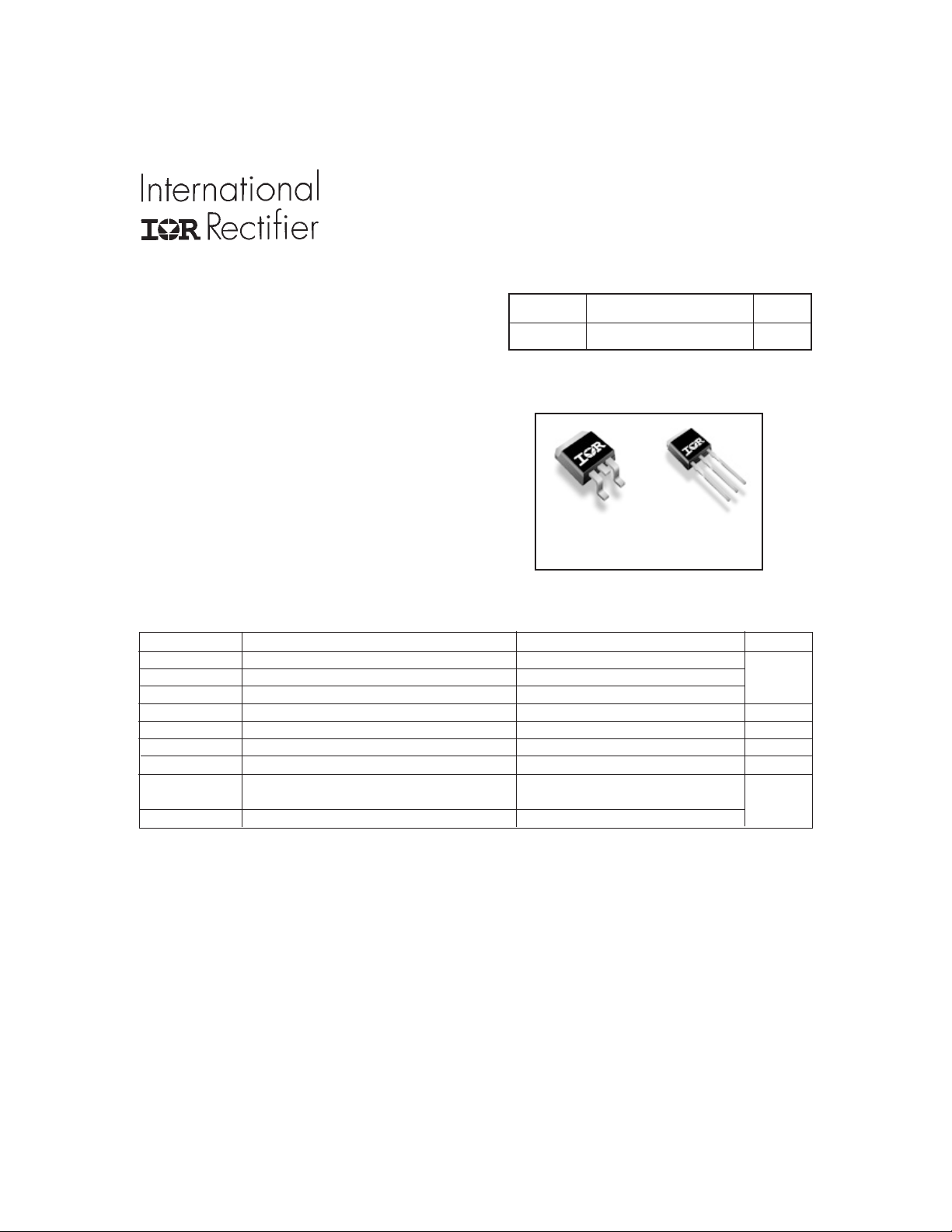
D2Pak
IRF3515S
TO-262
IRF3515L
°C
D
Applicable Off Line SMPS Topologies
l Telcom 48V input DC/DC Active Clamp Reset Forward Converter
Notes through are on page 10
www.irf.com 1
10/28/99
Page 2
IRF3515S/L
Static @ TJ = 25°C (unless otherwise specified)
Parameter Min. Typ. Max. Units Conditions
V
(BR)DSS
∆V
(BR)DSS
R
DS(on)
V
GS(th)
I
DSS
I
GSS
Dynamic @ TJ = 25°C (unless otherwise specified)
g
fs
Q
g
Q
gs
Q
gd
t
d(on)
t
r
t
d(off)
t
f
C
iss
C
oss
C
rss
C
oss
C
oss
C
eff. Effective Output Capacitance ––– 280 ––– VGS = 0V, VDS = 0V to 120V
oss
Avalanche Characteristics
E
AS
I
AR
E
AR
Thermal Resistance
R
θJC
R
θJA
Diode Characteristics
I
S
I
SM
V
SD
t
rr
Q
rr
t
on
2 www.irf.com
Drain-to-Source Breakdown Voltage 150 ––– ––– V VGS = 0V, ID = 250µA
/∆T
Breakdown Voltage Temp. Coefficient ––– 0.21 ––– V/°C Reference to 25°C, ID = 1mA
J
Static Drain-to-Source On-Resistance ––– ––– 0.045 Ω VGS = 10V, ID = 25A
Gate Threshold Voltage 3.0 ––– 4.5 V VDS = VGS, ID = 250µA
Drain-to-Source Leakage Current
––– ––– 25
––– ––– 250 VDS = 120V, VGS = 0V, TJ = 150°C
Gate-to-Source Forward Leakage ––– ––– 100 VGS = 30V
Gate-to-Source Reverse Leakage ––– ––– -100
VDS = 150V, VGS = 0V
µA
nA
VGS = -30V
Parameter Min. Typ. Max. Units Conditions
Forward Transconductance 15 ––– ––– S VDS = 50V, ID = 25A
Total Gate Charge ––– ––– 107 ID = 25A
Gate-to-Source Charge ––– ––– 23 nC VDS = 120V
Gate-to-Drain ("Miller") Charge ––– ––– 65 VGS = 10V, See Fig. 6 and 13
Turn-On Delay Time ––– 17 ––– VDD = 75V
Rise Time ––– 120 ––– ID = 25A
Turn-Off Delay Time ––– 34 ––– RG = 2.5Ω
ns
Fall Time ––– 63 ––– RD = 3.0Ω,See Fig. 10
Input Capacitance ––– 2260 ––– VGS = 0V
Output Capacitance ––– 530 ––– VDS = 25V
Reverse Transfer Capacitance ––– 170 ––– pF ƒ = 1.0MHz, See Fig. 5
Output Capacitance ––– 3330 ––– VGS = 0V, VDS = 1.0V, ƒ = 1.0MHz
Output Capacitance ––– 230 ––– VGS = 0V, VDS = 120V, ƒ = 1.0MHz
Parameter Typ. Max. Units
Single Pulse Avalanche Energy ––– 670 mJ
Avalanche Current ––– 25 A
Repetitive Avalanche Energy ––– 20 mJ
Parameter Typ. Max. Units
Junction-to-Case ––– 0.75 °C/W
Junction-to-Ambient ( PCB Mounted, steady-state)* ––– 40
Parameter Min. Typ. Max. Units Conditions
Continuous Source Current MOSFET symbol
(Body Diode)
Pulsed Source Current integral reverse
(Body Diode)
––– –––
––– –––
Diode Forward Voltage ––– ––– 1.3 V TJ = 25°C, IS = 25A, VGS = 0V
Reverse Recovery Time ––– 200 300 n s TJ = 25°C, IF = 25A
Reverse RecoveryCharge – –– 1.6 2.4 µC di/dt = 100A/µs
Forward Turn-On Time Intrinsic turn-on time is negligible (turn-on is dominated by LS+LD)
41
164
showing the
A
p-n junction diode.
G
D
S
Page 3
IRF3515S/L
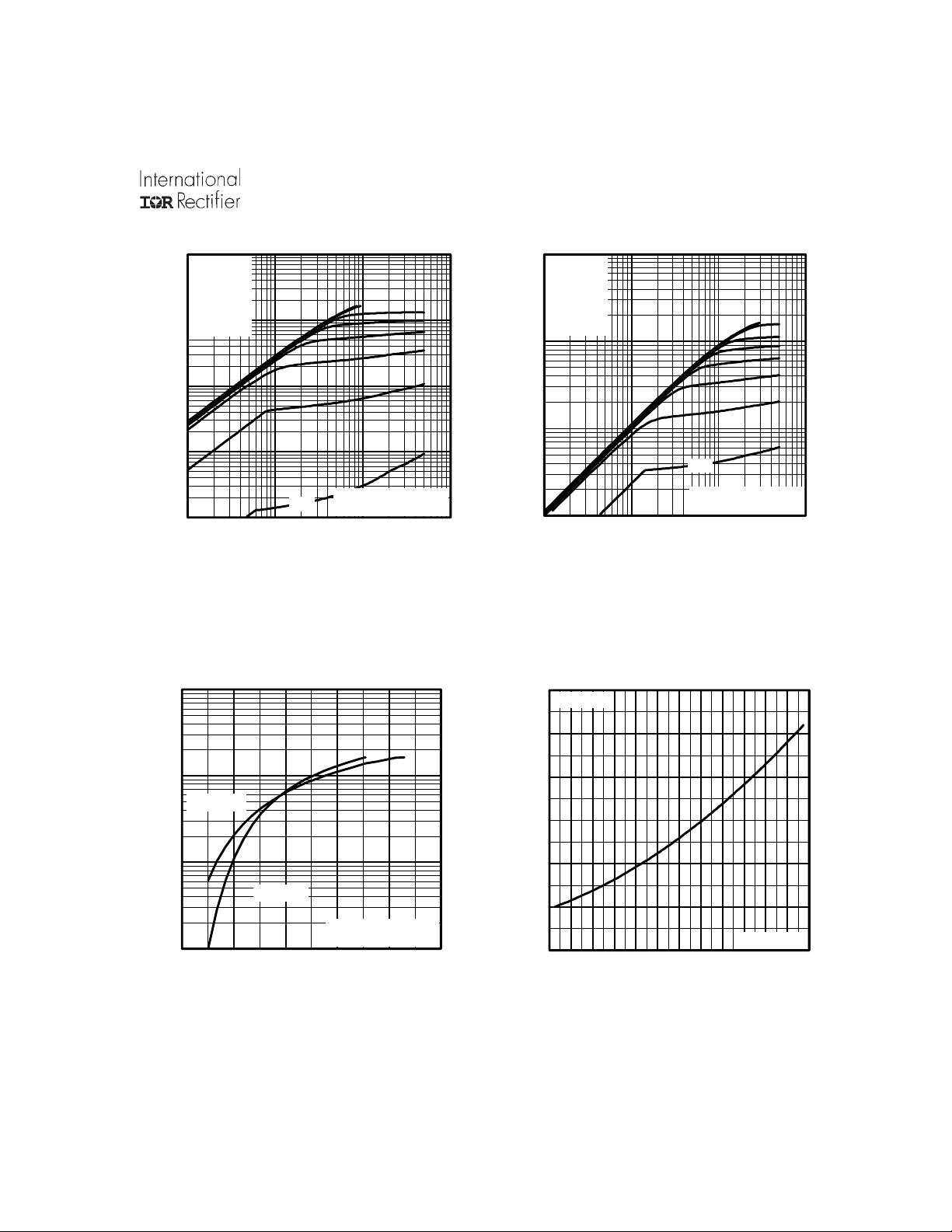
1000
100
10
1
D
I , Drain-to-Source Current (A)
0.1
0.1 1 10 100
1000
VGS
TOP
15V
12V
10V
9.0V
8.0V
7.0V
6.0V
BOTTOM
5.0V
5.0V
V , Drain-to-Source Voltage (V)
DS
20µs PULSE WIDTH
T = 25 C
J
°
1000
100
10
D
I , Drain-to-Source Current (A)
1
0.1 1 10 100
VGS
TOP
15V
12V
10V
9.0V
8.0V
7.0V
6.0V
BOTTOM
5.0V
5.0V
20µs PULSE WIDTH
T = 175 C
J
V , Drain-to-Source Voltage (V)
DS
°
Fig 2. Typical Output CharacteristicsFig 1. Typical Output Characteristics
3.0
I =
D
41A
2.5
100
°
T = 175 C
J
10
°
T = 25 C
D
I , Drain-to-Source Current (A)
1
4 6 8 10 12 14
J
V = 50V
DS
20µs PULSE WIDTH
V , Gate-to-Source Voltage (V)
GS
Fig 3. Typical Transfer Characteristics
2.0
1.5
(Normalized)
1.0
0.5
DS(on)
R , Drain-to-Source On Resistance
0.0
-60 -40 -20 0 20 40 60 80 100 120 140 160 180
T , Junction Temperature ( C)
J
Fig 4. Normalized On-Resistance
V =
GS
°
10V
Vs. Temperature
www.irf.com 3
Page 4

IRF3515S/L
100000
10000
V
= 0V, f = 1 MHZ
GS
C
= C
iss
gs
C
= C
rss
gd
C
= C
ds
+ C
oss
+ Cgd, C
gd
Ciss
1000
C, Capacitance(pF)
Coss
Crss
100
1 10 100
VDS, Drain-to-Source Voltage (V)
Fig 5. Typical Capacitance Vs.
Drain-to-Source Voltage
1000
SHORTED
ds
20
I =
25A
D
16
12
8
4
GS
V , Gate-to-Source Voltage (V)
V = 120V
DS
V = 75V
DS
V = 30V
DS
FOR TEST CIRCUIT
0
0 20 40 60 80 100 120
Q , Total Gate Charge (nC)
G
SEE FIGURE
Fig 6. Typical Gate Charge Vs.
Gate-to-Source Voltage
1000
OPERATION IN THIS AREA LIMITED
BY R
DS(on)
13
100
°
T = 175 C
J
10
°
T = 25 C
J
1
SD
I , Reverse Drain Current (A)
V = 0 V
0.1
0.2 0.6 1.0 1.4 1.8
V ,Source-to-Drain Voltage (V)
SD
GS
Fig 7. Typical Source-Drain Diode
100
10
D
I , Drain Current (A)I , Drain Current (A)
°
= 25 C
C
T T= 175 C
Single Pulse
1
1 10 100 1000
°
J
V , Drain-to-Source Voltage (V)
DS
Fig 8. Maximum Safe Operating Area
10us
100us
1ms
10ms
Forward Voltage
4 www.irf.com
Page 5

50
40
30
20
D
I , Drain Current (A)
10
0
25 50 75 100 125 150 175
T , Case Temperature ( C)
C
°
Fig 9. Maximum Drain Current Vs.
Case Temperature
IRF3515S/L
R
D.U.T.
t
d(off)tf
D
V
DS
V
GS
R
G
10V
Pulse Width ≤ 1 µs
Duty Factor ≤ 0.1 %
Fig 10a. Switching Time Test Circuit
V
DS
90%
10%
V
GS
t
d(on)tr
Fig 10b. Switching Time Waveforms
+
V
DD
-
1
D = 0.50
thJC
Thermal Response (Z )
0.001
0.20
0.1
0.10
0.05
0.02
0.01
0.01
0.00001 0.0001 0.001 0.01 0.1 1
SINGLE PULSE
(THERMAL RESPONSE)
t , Rectangular Pulse Duration (sec)
1
P
DM
Notes:
1. Duty factor D = t / t
2. Peak T = P x Z + T
1 2
J DM thJC C
t
1
t
2
Fig 11. Maximum Effective Transient Thermal Impedance, Junction-to-Case
www.irf.com 5
Page 6

IRF3515S/L
A
15V
DRIVER
+
-
V
R
20V
V
DS
G
t
L
D.U.T
I
AS
0.01
p
Ω
Fig 12a. Unclamped Inductive Test Circuit
V
(BR)DSS
t
p
I
AS
Fig 12b. Unclamped Inductive Waveforms
Q
G
10 V
Q
GS
Q
GD
DD
1600
TOP
1200
800
400
AS
E , Single Pulse Avalanche Energy (mJ)
0
25 50 75 100 125 150 175
Starting T , Junction Temperature ( C)
J
BOTTOM
Fig 12c. Maximum Avalanche Energy
Vs. Drain Current
I
°
D
10A
17A
25A
V
G
Charge
Fig 13a. Basic Gate Charge Waveform
Current Regulator
Same Type as D.U.T.
50KΩ
.2µF
12V
V
GS
.3µF
D.U.T.
3mA
I
G
Current Sampling Resistors
+
V
DS
-
I
D
Fig 13b. Gate Charge Test Circuit
6 www.irf.com
Page 7

IRF3515S/L
Peak Diode Recovery dv/dt Test Circuit
D.U.T
+
Circuit Layout Considerations
• Low Stray Inductance
• Ground Plane
• Low Leakage Inductance
Current Transformer
-
+
-
-
+
R
G
Driver Gate Drive
P.W.
• dv/dt controlled by R
• Driver same type as D.U.T.
G
• ISD controlled by Duty Factor "D"
• D.U.T. - Device Under Test
Period
D =
Period
P.W.
+
-
VGS=10V
V
DD
*
D.U.T. ISDWaveform
Reverse
Recovery
Current
Re-Applied
Voltage
D.U.T. VDSWaveform
Inductor Curent
* V
= 5V for Logic Level Devices
GS
Fig 14. For N-Channel HEXFET
Body Diode Forward
Current
di/dt
Diode Recovery
dv/dt
Body Diode Forward Drop
Ripple ≤ 5%
V
DD
I
SD
®
Power MOSFETS
www.irf.com 7
Page 8

IRF3515S/L
A
D2Pak Package Outline
10.54 (.415)
1.40 (.055)
MAX.
1.78 (.070)
1.27 (.050)
1.40 (.055)
3X
1.14 (.045)
5.08 (.200)
NOTE S:
1 DIMENSIONS AFTER SOLDER DIP.
2 DIMENSIONING & TOLERANCING PER ANSI Y14.5M , 1982.
3 CONTROLLING DIMENSION : INCH.
4 HEATSINK & LEAD DIMENSIONS DO NOT INCLUDE BURRS.
10.29 (.405)
- A 2
1 3
15.49 (.610)
14.73 (.580)
0.93 (.037)
3X
0.69 (.027)
0.25 (.0 1 0) M B A M
4.69 (.185)
4.20 (.165)
D2Pak Part Marking Information
5.28 (.208)
4.78 (.188)
0.55 (.022)
0.46 (.018)
- B -
1.32 (.052)
1.22 (.048)
2.79 (.110)
2.29 (.090)
1.39 (.055)
1.14 (.045)
LEAD ASSIGNM E N TS
1 - G ATE
2 - D RA IN
3 - SOURCE
10.16 (.400)
REF .
6.47 (.255)
6.18 (.243)
2.61 (.103)
2.32 (.091)
8.89 (.350)
REF .
MINIMUM RECOMMENDED FOOTPRINT
11.43 (.450)
8.89 (.350)
17.78 (.700)
3.81 (.150)
2.08 (.082)
2X
2.54 (.100)
2X
INTERNATIONAL
RE CTIFIE R
LO G O
A S SEMBLY
LO T CO D E
F530S
9246
9 B 1M
PART NUM B ER
DATE CODE
(YYW W )
YY = YEAR
WW = WEEK
8 www.irf.com
Page 9

TO-262 Package Outline
IRF3515S/L
TO-262 Part Marking Information
www.irf.com 9
Page 10

IRF3515S/L
D2Pak Tape & Reel Information
TRR
FEED DIRECTION
TRL
FEED DIRECTION
1.85 (.073)
1.65 (.065)
10.90 (.429)
10.70 (.421)
1.60 (.063)
1.50 (.059)
4.10 (.161)
3.90 (.153)
11.60 (.457)
11.40 (.449)
16.10 (.634)
15.90 (.626)
1.60 (.063)
1.50 (.059)
1.75 (.069)
1.25 (.049)
15.42 (.609)
15.22 (.601)
0.368 (.0145)
0.342 (.0135)
24.30 (.957)
23.90 (.941)
4.72 (.136)
4.52 (.178)
13.50 (.532)
12.80 (.504)
330.00
(14.173)
MAX.
NOTES :
1. COM FORMS TO EIA-418.
2. CONTROLLING DIMENSION: MILLIMETER.
3. DIMENSION MEASURED @ HUB.
4. INCLUDES FLANGE DISTORTION @ OUT ER EDGE.
27.40 (1.079)
23.90 (.941)
4
26.40 (1.039)
24.40 (.961)
3
60.00 (2.362)
MIN.
30.40 (1.197)
MA X.
4
Notes:
Repetitive rating; pulse width limited by
Pulse width ≤ 300µs; duty cycle ≤ 2%.
max. junction temperature. (See fig. 11)
C
eff. is a fixed capacitance that gives the same charging time
Starting T
RG = 25Ω, I
I
SD
= 25°C, L = 2.2mH
J
AS
≤ 5.0A, di/dt ≤ 330A/µs, V
= 25A. (See Figure 12)
≤ V
DD
(BR)DSS
,
oss
as C
oss
while V
is rising from 0 to 80% V
DS
DSS
TJ ≤ 175°C
* When mounted on FR-4 board using minimum recommended footprint.
For recommended footprint and soldering techniques refer to application note #AN-994.
WORLD HEADQUARTERS: 233 Kansas St., El Segundo, California 90245, Tel: (310) 322 3331
IR GREAT BRITAIN: Hurst Green, Oxted, Surrey RH8 9BB, UK Tel: ++ 44 1883 732020
IR CANADA: 15 Lincoln Court, Brampton, Ontario L6T3Z2, Tel: (905) 453 2200
IR GERMANY: Saalburgstrasse 157, 61350 Bad Homburg Tel: ++ 49 6172 96590
IR ITALY: Via Liguria 49, 10071 Borgaro, Torino Tel: ++ 39 11 451 0111
IR JAPAN: K&H Bldg., 2F, 30-4 Nishi-Ikebukuro 3-Chome, Toshima-Ku, Tokyo Japan 171 Tel: 81 3 3983 0086
IR SOUTHEAST ASIA: 1 Kim Seng Promenade, Great World City West Tower, 13-11, Singapore 237994 Tel: ++ 65 838 4630
IR TAIWAN:16 Fl. Suite D. 207, Sec. 2, Tun Haw South Road, Taipei, 10673, Taiwan Tel: 886-2-2377-9936
Data and specifications subject to change without notice. 10/99
10 www.irf.com
 Loading...