

Page 1
R
Overview
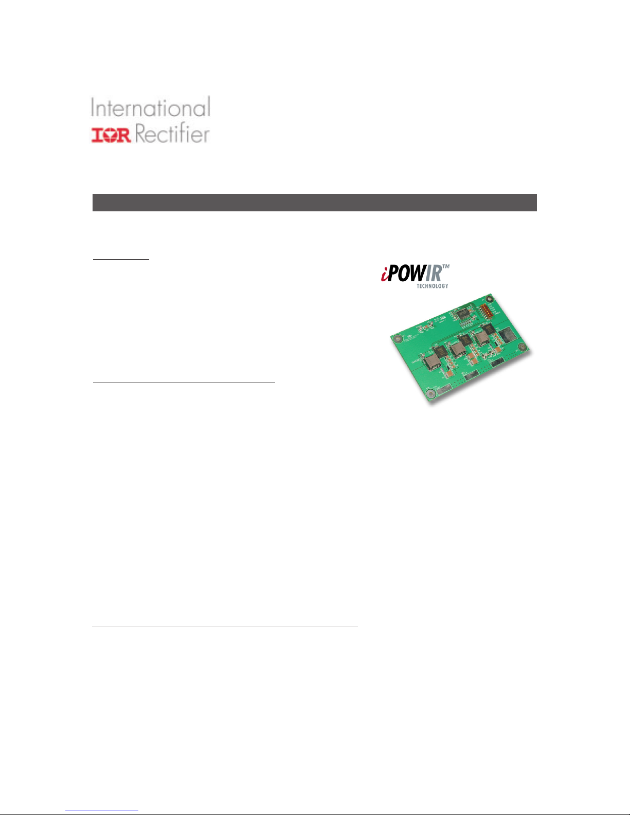
In this document, table 1 and figure 1 are provided to enable engineers to
easily evaluate the iP2001 in a 3-phase configuration that is capable of
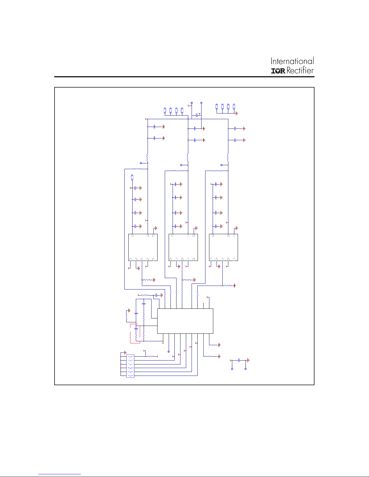
providing up to 60A in a lab environment without airflow. Figures 3, 4, 5 and
6 and the complete bill of materials in table 2 are provided as a reference
design to enable engineers to very quickly and easily design a 3-phase
converter. In order to optimize this design to your specific requirements
refer to the data sheet for the controller listed in the bill of materials. A variety
of other controllers may also be used, but the design will require layout and
control circuit modifications.
Demoboard Quick Start Guide
Initial Settings:
z The output is set to 1.7V, but can be adjusted from 1.1 to 1.85V by setting
z The switching frequency per phase is set to 500kHz with the frequency set resistor R4. This creates an effective
Procedure for Connecting and Powering Up Demoboard:
1. Apply input voltage (5-12V) across VIN (TP18) and PGND (TP14). Note that this input source must be applied first during
2. Apply +5V logic power across +5V (TP19) and PGND (TP20).
3. Apply load across VOUT pads (TP10 - TP12) and PGND pads (TP14 - TP16)
4. Set ENABLE high.
5. Monitor switch node signals (optional) via TP6 - TP8.
6. Adjust load accordingly.
EFERENCE
R
EFERENCE
International Rectifier • 233 Kansas Street, El Segundo, CA 90245 USA
IRDCiP2001-B, 500kHz, 60A, 3-phase Synchronous Buck
S1 according to the VID codes provided in Table 1. Droop control is set to 50mV at 60A, but can be adjusted by
following the instructions in the data sheet for the PWM controller.
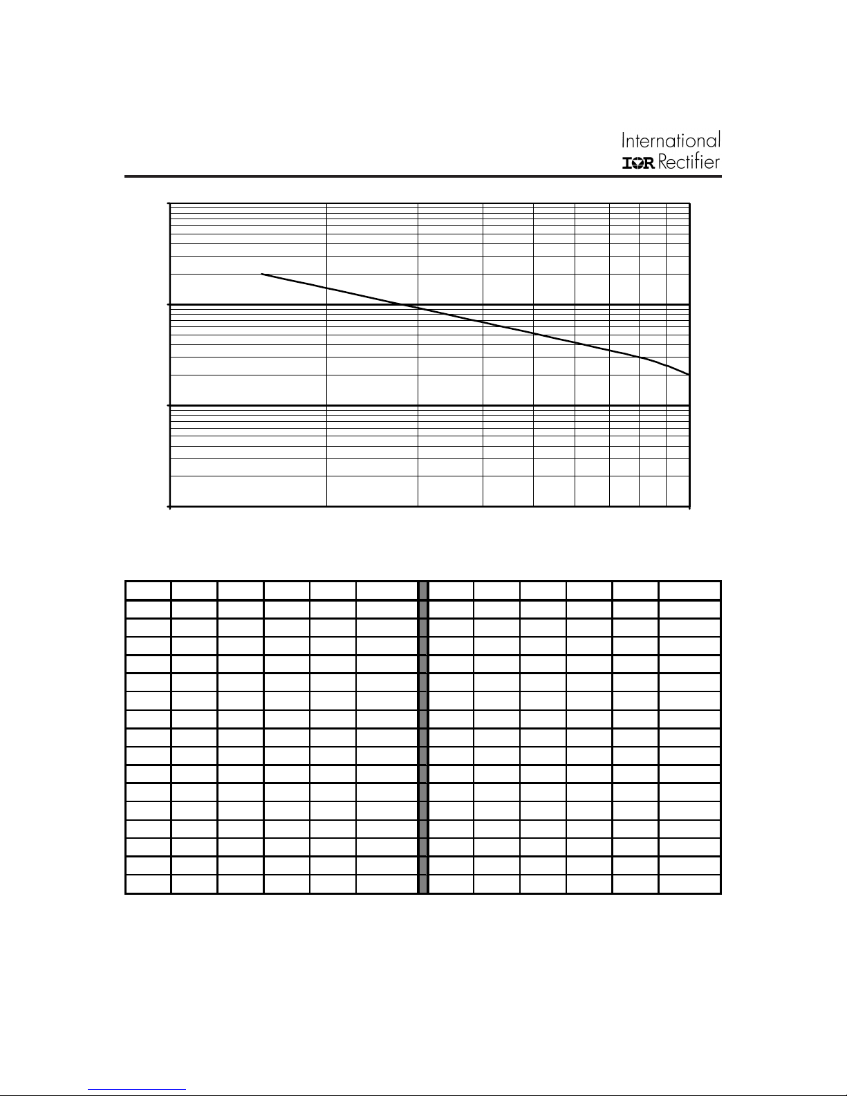
output frequency of 1.5MHz. The graph in figure 1 shows the relationship between R4 and the switching frequency
per phase. This frequency may be adjusted by changing R4 according to this graph; however, extreme changes
from the 500kHz set point may require redesigning the control loop and adjusting the values of input and output
capacitors. Also, refer to the SOA graph in the iP2001 datasheet for maximum operating current at different
frequencies.
the power-up sequence.
D
D
Converter using iP2001
ESIGN
ESIGN
IRDCiP2001-B
iP2001 Recommended Operating Conditions
(refer to the iP2001 datasheet for maximum operating conditions)
Input voltage: 5 - 12V
Output voltage: 1.1 - 1.85V
Output current: 20A per phase, 60A total for 3-phase demo board.
Switching Freq: 500kHz per phase, 1.5MHz effective output frequency.
07/19/02
Page 2
IRDCiP2001-B
1000
100
)
Ω
Resistance (k
10
1
100 1000
Output Frequency (kHz)
Figure 1 - R4 vs. Frequency per Phase
VID4 VID3 VID2 VID1 VID0 VDAC VID4 VID3 VID2 VID1 VID0 VDAC
11111 Off 011111.475
111101.100 011101.500
111011.250 011011.525
111001.150 011001.550
110111.175 010111.575
110101.200 010101.600
110011.225 010011.625
110001.250 010001.650
101111.275 001111.675
101101.300 001101.700
101011.325 001011.725
101001.350 001001.750
100111.375 000111.775
100101.400 000101.800
100011.425 000011.825
100001.450 000001.850
Table 1 - PWM IC Voltage Identification Codes
www.irf.com2
Page 3
IRDCiP2001-B
92%
90%
88%
fSW= 500kHz
86%
VIN = 12V
= 1.6V
V
OUT
= 25°C
T
A
0 102030405060
fSW= 1MHz
84%
82%
80%
Efficiency
Output Current (A)
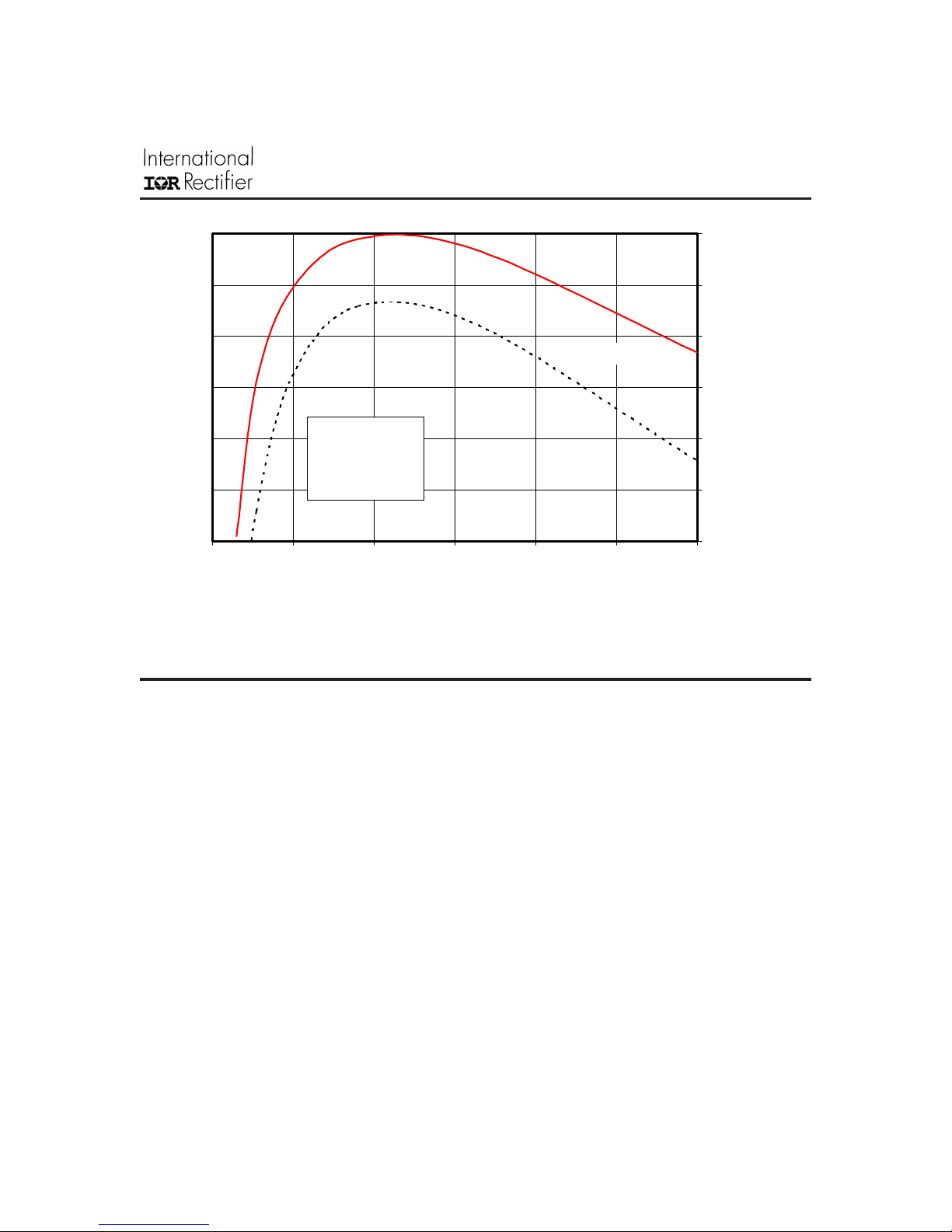
Figure 2 - Typical Efficiency vs. Current
Refer to the following application notes for detailed guidelines and suggestions when
implementing iPOWIR Technology products:
AN-1028: Recommended Design, Integration and Rework Guidelines for International Rectifier’s
iPOWIR Technology BGA Packages
This paper discusses the assembly considerations that need to be taken when mounting iPOWIR BGA’s
on printed circuit boards. This includes soldering, pick and place, reflow, inspection, cleaning and
reworking recommendations.
AN-1029: Optimizing a PCB Layout for an iPOWIR Technology Design
This paper describes how to optimize the PCB layout design for both thermal and electrical performance.
This includes placement, routing, and via interconnect suggestions.
AN-1030: Applying iPOWIR Products in Your Thermal Environment
This paper explains how to use the Power Loss and SOA curves in the data sheet to validate if the
operating conditions and thermal environment are within the Safe Operating Area of the iPOWIR product.
www.irf.com 3
Page 4
IRDCiP2001-B
VOUT
TP22
TP14
PGND
TP15
PGND
TP17
PGND
TP16
VOUT
C17
100uF
C16
Open
VOUT SENSE
C33
0.01uF X7R
VOUT SENSENE
C20
100uF
C19
100uF
PGND SENSE
PGNDSENSE
TP21
TP13
VOUT
TP12
VOUT
TP11
VOUT
TP10
PGND
C23
100uF
C22
Open
L1
0.54uH
TP6
SWNODE1
R5
2K 1%
TP18
Vin
C30
10uF
Vin
C5
10uF
C4
10uF
C3
10uF
VIN
VIN
VSW1
VSW1
IP2001 U2
VDD
SGND
PWM1
ENABLE
VDD
SGND
PWM1
ENABLE
+5V
ENABLE SWNODE1
R15
10K
0
R14
+5V
C1
0.022uF
22pF
C28
R1
R3
7
8
9
10
11
12
1k
open
Cx
4700pF
R2
1K
Rx
51
Rx &Cx are not parts of PCB
*
S1
R6
ENABLE
6
5
4
3
2
1
U3
PGND
PGND
IP2001
PRDY
PRDY
+5V
C2
10uF
20
16
VCC
ISEN1
COMP
6
FB
7
VSEN
U1
10
TP5
10K
VOUT SENSE
+5V
TP7
SWNODE2
R7
2K 1%
C31
10uF
Vin
C8
10uF
C7
10uF
C6
10uF
VIN
VIN
VDD
SGND
PWM2
VDD
SGND
PWM2
R10
0
R11
15
14
13
ISEN2
PWM1
PWM2
VID4
VID3
PGOOD19VID2
1
2
PGOOD
VID2
VID3
VID4
SWNODE2
ENABLE
0
3
L2
0.54uH
U4
VSW2
PGND
VSW2
PGND
ENABLE
ENABLE
R16
VID1
IP2001
PRDY
PRDY
+5V
10K
R12
0
+5V
18
11
17
12
ISEN4
ISEN3
PWM3
VID1
VID0
FS/DIS
4
5
8
9
VID0
PWM4
GND
R4
Freq. Set Resistor
L3
0.54uH
TP8
SWNODE3
R8
2K 1%
C32
10uF
Vin
C11
10uF
C10
10uF
C9
10uF
SWNODE3
VIN
VIN
VSW3
PGND
VSW3
PGND
VDD
SGND
PWM3
ENABLE
SGND
PRDY
PWM3
ENABLE
PRDY
ENABLE
R17
10K
Note: Rx and Cx are add on components
*
C27
10uF
+5V
TP19
TP20
+5V
PGND
VDD
HIP6311
51K
Fig. 3 - Reference Design Schematic
www.irf.com4
Page 5
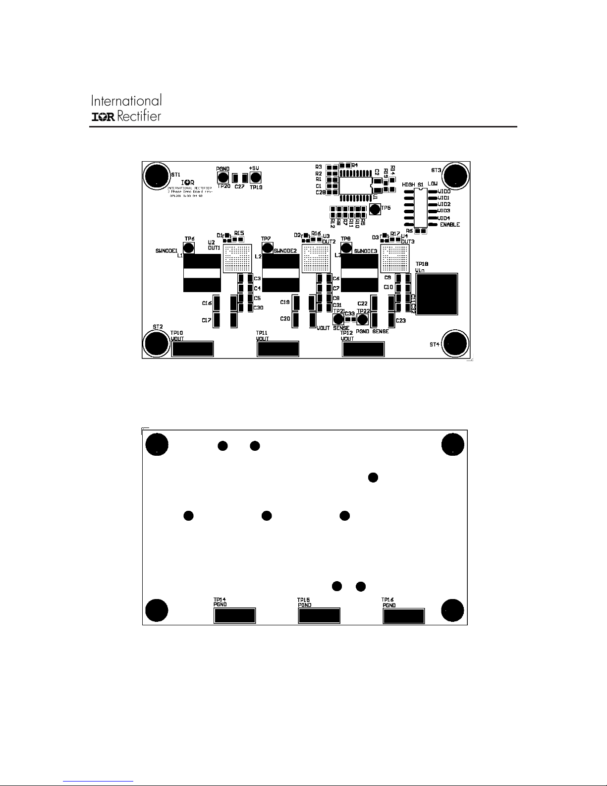
Fig. 4 - Component Placement Top Layer
IRDCiP2001-B
www.irf.com 5
Fig. 5 - Component Placement Bottom Layer
Page 6
IRDCiP2001-B
r
V
K
K
p
K
K
A
A
p
y
r
Designato
alue 1Value 2 Type Toler ance Package Mfr. Mfr. Part No.
C1 0.022uF 50V X7R 10% 0805 TDK C2012X7R1H223
C2 - C11, C27, C30 - C32 10.0uF 16V X5R 10% 1210 T DK C3225X5R1C106
C16, C22, D1 - D3, R3, R19 - - - - - - -
C17, C19, C20, C23 100uF 6.3V X5R 10% 2220 T DK C5750X5R0J107K
C28 22.0
F 50V COG 5% 0805 TDK C2012COG1H220J
C33 0.010uF 50V X7R 10% 0805 TDK C2012X7R1H103
Cx 4700pF 50V X7R 10% 0603 T DK C1608X7R1H472
L1 - L3 0.54uH 27A Ferrite 20% SMT Panasonic ETQP6F0R6BF
R1, R2 1K 1/8W Thick fi lm 5% 0805 ROHM MCR10EZHJ102
R10 - R12, R14 0 1/8W Thick film <50m 0805 ROHM MCR10EZHJ000
R6, R15 - R17 10K 1/8W Thick fil m 5% 0805 ROHM MCR10EZHJ103
R4 51K 1/8W T hick film 5% 0805 ROHM MCR10EZHJ513
R5, R7, R8 2K 1/8W Thick fi lm 5% 0805 ROHM MCR10EZHJ202
Rx 51 1/10W Thick film 5% 0603 KO
S1 SPST 6
osition Switch - SMT C&K Components SD06H0SK
ST1 - ST4 4-40 - - - - Ke
U1 - - PWM controlle
0 - 70°C SOIC20 Intersil HIP6311CB
stone 8412
RM73B1J510J
U2 - U4 - - DC-DC - 11 x 11 x 3mm IR IP2001
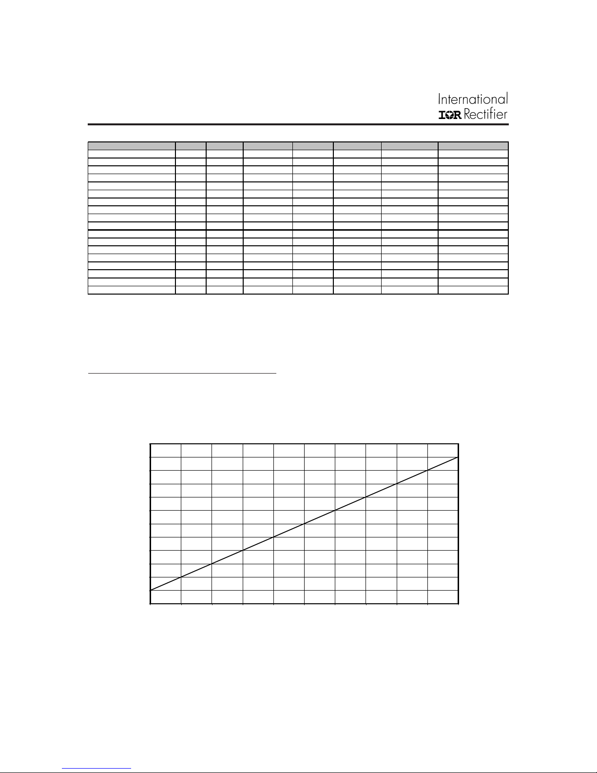
Table 2 - Reference Design Bill of Materials
Adjusting the Over-Current Limit
R7 & R8 are the resistors used to adjust the over-current trip point. The trip point is a function of the controller and
corresponds to 165% of the output current indicated on the x-axis of Fig. 6. For example, selecting a resistance of 1.5K
at each phase will set the trip point to 165% of 15A, or 24.75A. The trip point for each phase on the demoboard is currently
set to 165% of 20A, or 33A.
2100
2000
1900
1800
1700
1600
)
:
(
1500
ISEN
R
1400
1300
1200
1100
1000
900
10 11 12 13 14 15 16 17 18 19 20
Fig. 6 - R
Output Current (A)
vs Current (per Phase)
ISEN
www.irf.com6
Page 7
IRDCiP2001-B
Sequencing Tip
It’s important to have proper sequencing between the control IC and the iP2001 blocks. This assures the soft-start
routine of the IC will properly ramp-up the output voltage during a power-up or restart from shut down event. Figure
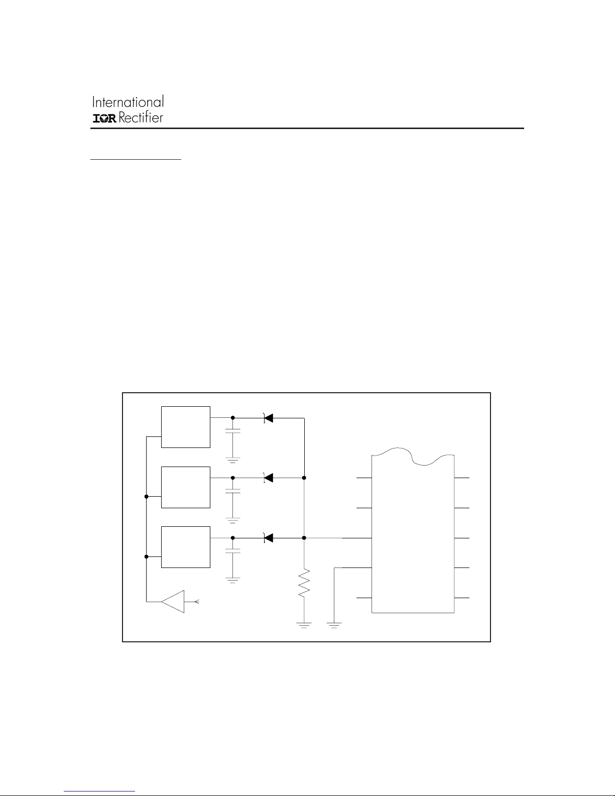
7 shows a simple and cost effective way to synchronize the iP2001 blocks with an HIP6311 control IC in a 3 Phase
configuration.
Placing Schottky diodes between the iP2001’s PRDY pin and the IC’s FS/DIS pin creates an interface analogous to an
AND operation. With this configuration, no single iP2001 can enable the IC independently. This configuration also
resolves any differences in timing and logic thresholds between iP2001 devices. The capacitors are used to filter
high frequency noise on the PRDY line. Additionally, the ENABLE pin of the iP2001 blocks can be used as the master
control switch for the system.
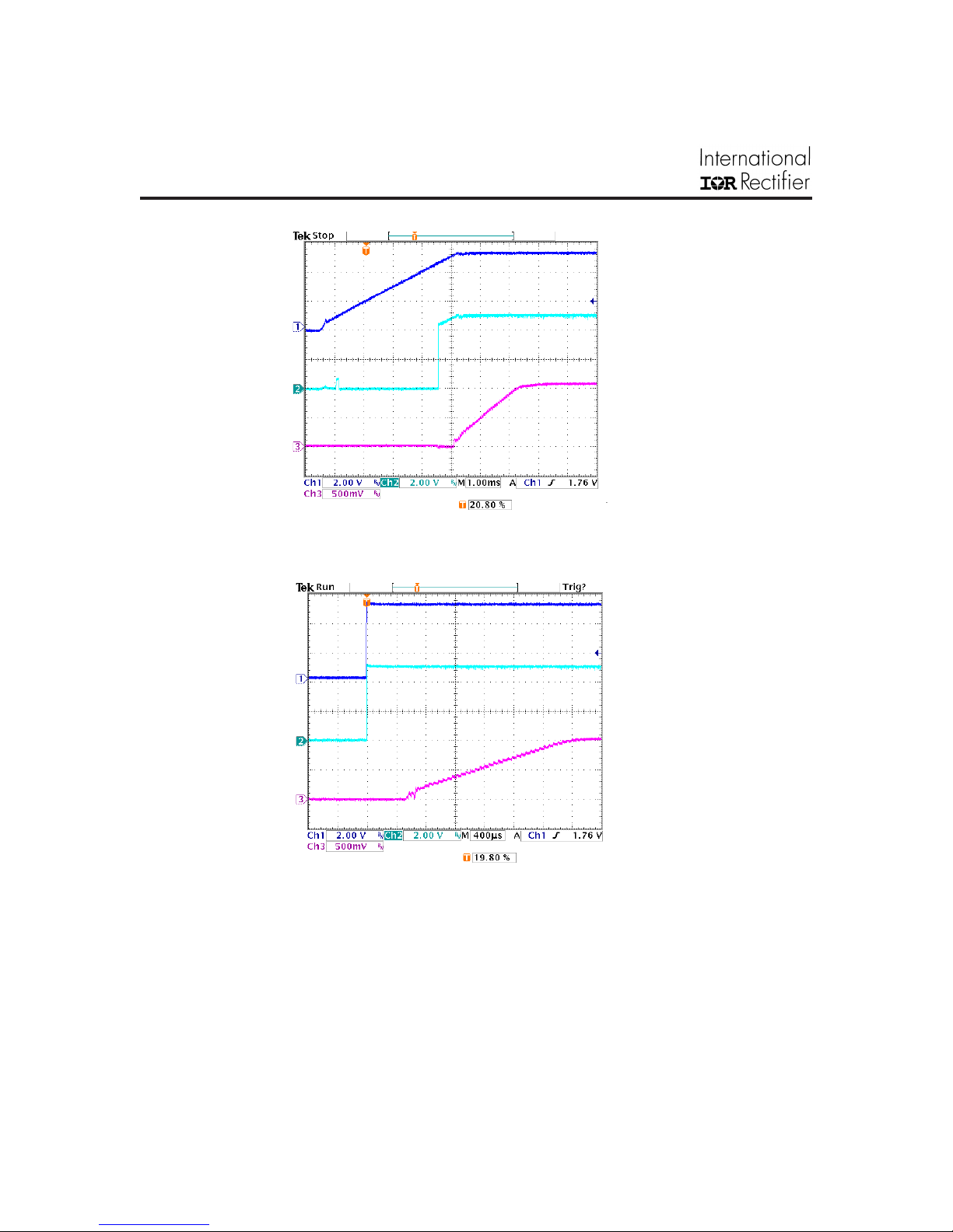
During power-up, the PRDY pin is held low until VDD reaches a typical voltage of 4.4V. Until then, the schottky diode is
forward biased and clamps the FS/DIS pin well below the disable voltage of the HIP6311 IC (typically 1V). Upon
reaching 4.4V, the PRDY pin transitions to a logic-level high state and releases the clamp on the FS/DIS pin. This
enables the IC and allows its soft start routine to begin (see figure 8), assuming the voltage at the IC’s VCC pin is
greater than its power-on reset threshold.
When the ENABLE pin is held to a logic-level low state (shut down mode), the PRDY pin clamps the FS/DIS pin of the
IC below the disable voltage. After the ENABLE pin transitions to a logic-level high state, the PRDY releases the
clamp on the FS/DIS pin, enabling the IC and allowing its soft start routine to begin (see figure 9).
During power-down, the PRDY pin transitions to a logic-level low state when the VDD reaches the under voltage lock
out threshold of the iP2001 blocks. The FS/DIS pin is then clamped below the disable voltage, disabling the control IC.
BAT54
PRDY1
ENABLE
0.22µF
iP2001
BAT54
PRDY2
ENABLE
iP2001
0.22µF
COMP
FB
PWM1
PWM2
BAT54
PRDY3
ENABLE
iP2001
0.22µF
51k
Master
FS/DIS
GND
VSEN
ISEN2
ISEN3
PWM3
Control
HIP6311
Fig. 7 - Sequencing Schematic
www.irf.com 7
Page 8
IRDCiP2001-B
Fig. 8 - VDD Rise vs. Output Timing
Ch 1: V
DD
Ch 2: PRDY
Ch 3: V
OUT
Ch 1: ENABLE
Ch 2: PRDY
Ch 3: V
OUT
Fig. 9 - Enable On vs. Output Timing
Use of this design for any application should be fully verified by the customer. International
Rectifier cannot guarantee suitability for your applications, and is not liable for any result of
usage for such applications including, without limitation, personal or property damage or
violation of third party intellectual property rights.
IR WORLD HEADQUARTERS: 233 Kansas St., El Segundo, California 90245, USA Tel: (310) 252-7105
TAC Fax: (310) 252-7903
www.irf.com8
 Loading...