

Page 1

IRU3073 EVALUATION BOARD USER GUIDE
SPECIFICATION DATAINTRODUCTION
The IRU3073 controller IC is designed to provide a low
cost synchronous Buck regulator for on-board DC to DC
converter for multiple output applications.
The outputs can be programmed as low as 0.8V for low
voltage applications.
Selectable over-current protection is provided by using
external MOSFET's on-resistance for optimum cost and
performance.
This device features a programmable frequency set from
200KHz to 400KHz, under-voltage lockout for all input
supplies, an external programmable soft-start function
as well as output under-voltage detection that latches off
the device when an output short is detected.
Switcher:
VIN = 5V
VOUT1 = 2.5V
IOUT1 = 8A
DVOUT = 50mV
FS = 200KHz
IRDC3073EVAL
Linear
Regulator:
VIN = 2.5V
(from switch)
VOUT2 = 1.6V
IOUT2 = 2A
Supply Voltage:
VCC = VC = 12V
INPUT/OUTPUT CONNECTIONS
The following is the input/output connections:
Inputs:
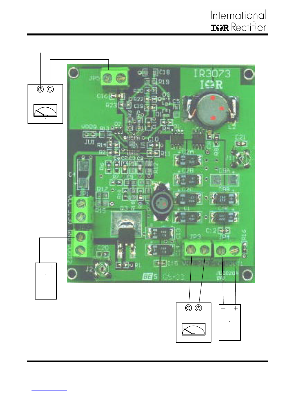
JP3: Input (+5V), Gnd
JP1: Input (+12V)
Outputs:
JP4: VOUT1 (+2.5V), Gnd
JP2: VOUT2 (+1.6V), Gnd
Note: For proper operation, +5V supply should ramp up first.
The connection points is shown in Figure 1. Connect the
power supply cables according to this figure, minimize
wire lengths to reduce losses in the wire. Test point J1
provides easy connections for the oscilloscope voltage
probe to monitor the output voltage.
Rev. 1.0
06/30/03
www.irf.com
1
Page 2
IRDC3073EVAL
CONNECTION DIAGRAM
Gnd
+12V
Power Supply
1A Supply
Load2
2A
Figure 1 - Connection diagram of evaluation-board for IRU3073.
2
www.irf.com
Gnd
+5V
Power Supply
10A Supply
Load1
0 - 10A
Rev. 1.0
06/30/03
Page 3
LAYOUT
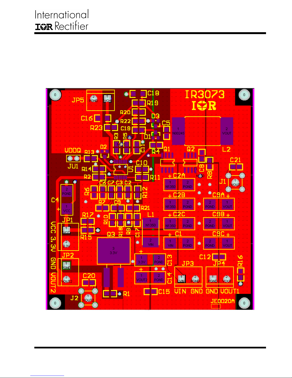
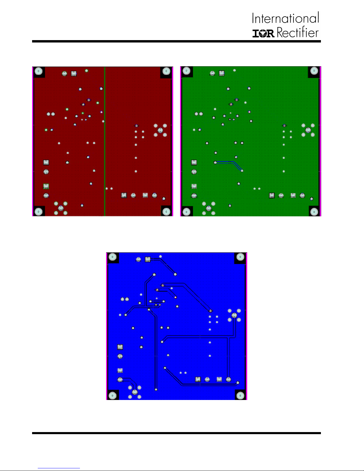
The four layers for IRU3073 evaluation board are shown
in Figures 2.1-2.4. The layout is designed both for direct
FET package and SOIC package for power MOSFETs.
The input capacitors are all located close to the
MOSFETs. All the decoupling capacitors and feedback
components are located close to IC. The feedback re-
IRDC3073EVAL
sistors are tied to the output voltage at the point of regulation.
The middle layers are dedicated to Power Ground and
Analog Ground. Analog Ground is kept separated from
the Power Ground and it is connected at a single point
as shown in figure 2.3.
Figure 2.1 - Top layer of evaluation-board for IRU3073.
Rev. 1.0
06/30/03
www.irf.com
3
Page 4
IRDC3073EVAL
LAYOUT
Figure 2.2 - Middle layer 1. Figure 2.3 - Middle layer 2.
4
Figure 2.4 - Bottom layer.
www.irf.com
Rev. 1.0
06/30/03
Page 5
SCHEMATIC
IRDC3073EVAL
Rev. 1.0
06/30/03
www.irf.com
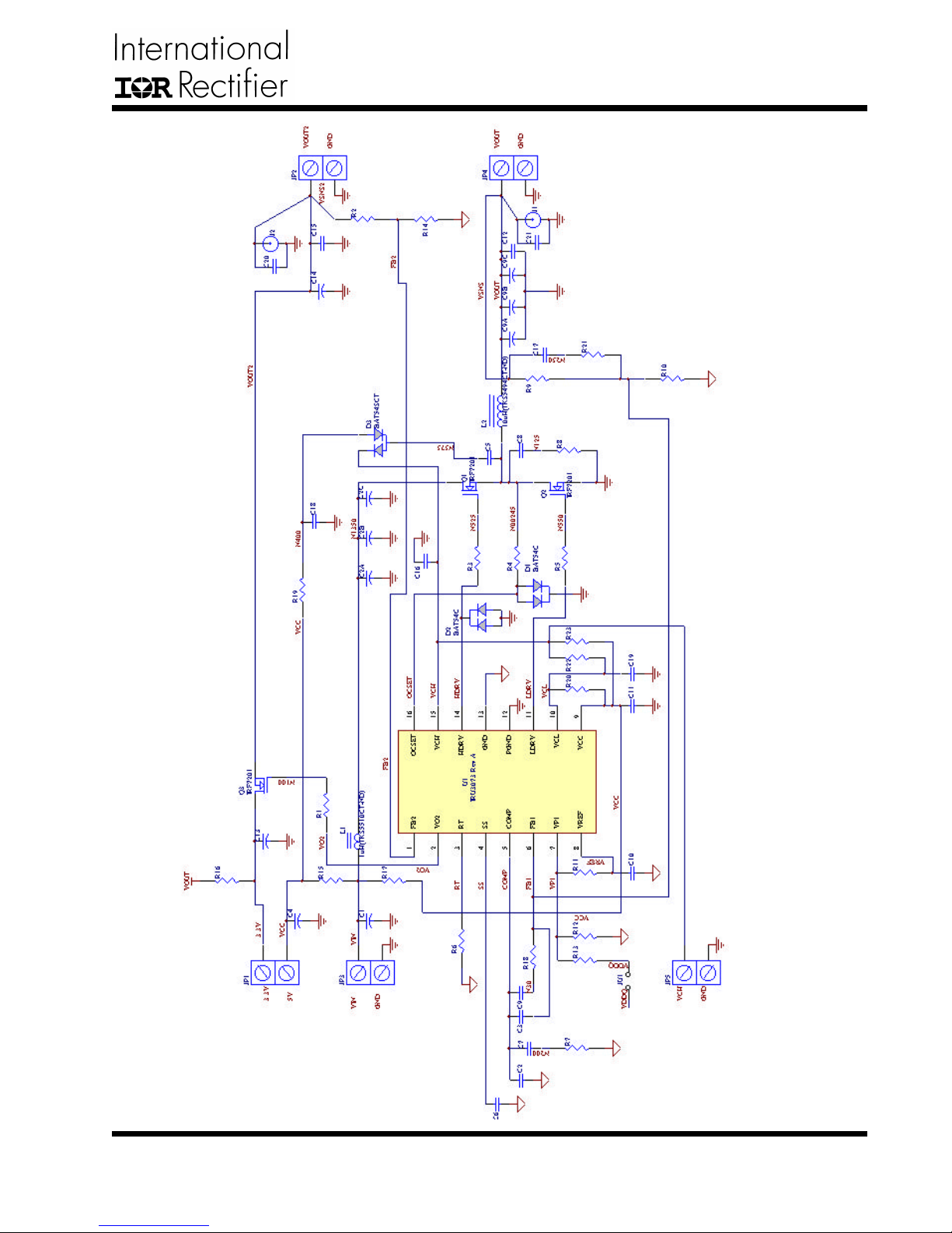
Figure 3 - Schematic of evaluation-board for IRU3073.
5
Page 6
IRDC3073EVAL
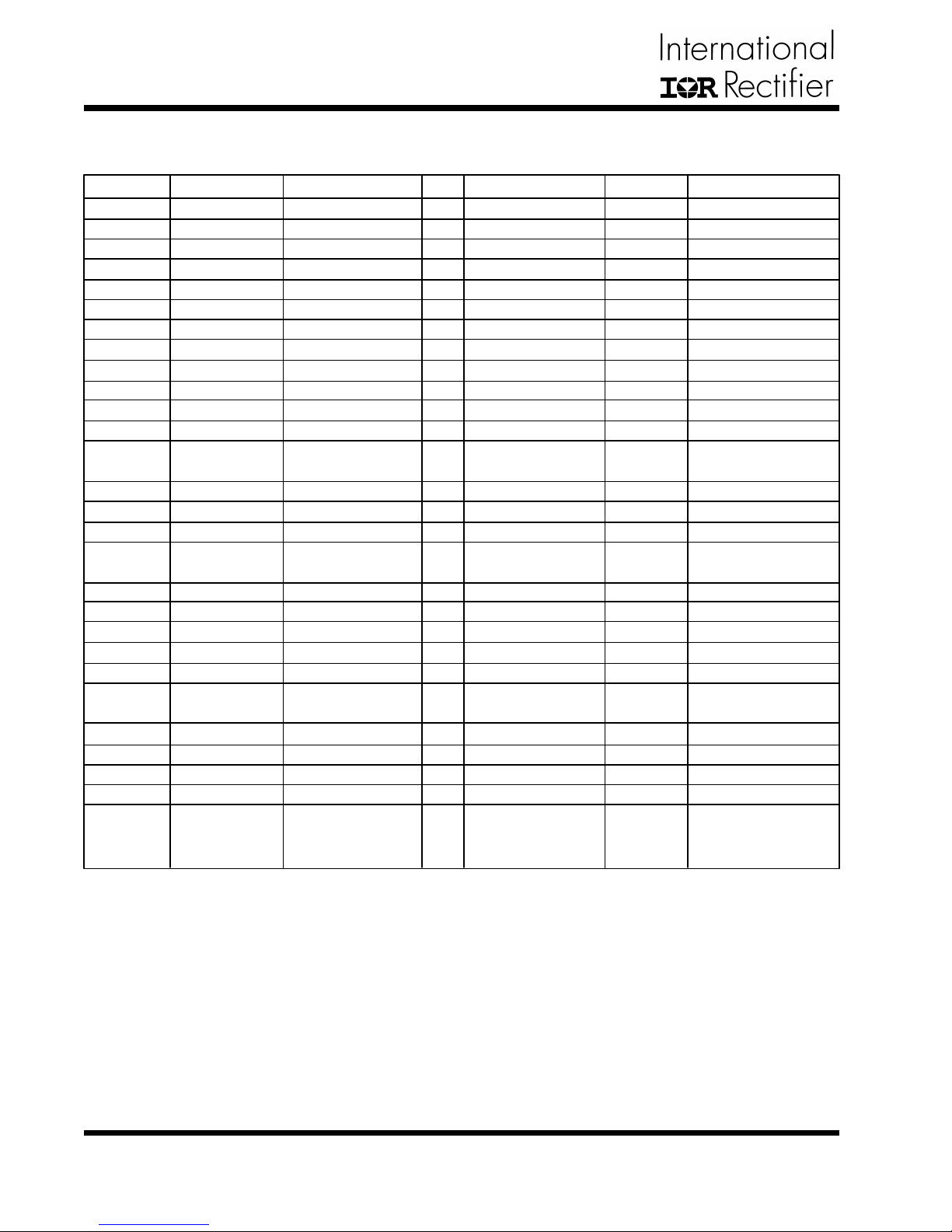
BILL OF MATERIAL
Ref Desig Description Value Qty Part# Manuf Web site (www.)
Q1,Q2
Q3
U1
D2
L1
L2
C1,C2A,B,C
C2
C6,C10
C7
C8
C9B,C
C11,12,15,
16,19,20,21
C13,C14
R1
R2,10,14
R3,5,11,16,
20,22,23
R4
R6
R7
R8
R9
R12,13,15,
17,18,19,21
C3,4,5,9,17
D1,D3
JP1,2,3,4,5
J1,J2
Circuit
Board
Spacer
MOSFET
MOSFET
Controller
Schottky Diode
Inductor
Inductor
Cap, Poscap
Cap, Ceramic
Cap, Ceramic
Cap, Ceramic
Cap, Ceramic
Cap, Poscap
Cap, Ceramic
Cap, Poscap
Resistor
Resistor
Resistor
Resistor
Resistor
Resistor
Resistor
Resistor
Resistor
Capacitor
Diode
Connector
Scope Probe
Spacer
1mH, 5.6A
3.3mH, 17A
47mF, 16V
33pF, NPO, 5%
0.1mF, Y5V, 25V
2200pF, X7R, 50V
470pF, X7R, 50V
330mF, 40mV
1mF, Y5V, 16V
150mF, 6.3V
10V
1K, 1%
0V
5.1K, 1%
100K
24K, 1%
4.7V, 1%
2.15K, 1%
NA (Open)
NA (Open)
NA (Open)
2-Pos Terminal
Bumpon
2
IRF7832
1
IRLR2703
1
IRU3073CQ
1
BAT54
1
DO3316P-102
1
DO5022P-332HC
4
16TPB47M
1
ECU-V1H330JCV
2
ECJ-2VF1E104
1
ECU-V1H222KBV
1
ECJ-2VC1H471J
2
6TPB330M
7
ECJ-2VF1C1O5Z
2
6TPB150M
1
3
7
1
1
1
1
1
7
5
2
5
ED1973-ND
2
131-5031-00
4
SJ-67A3 Black
IR
IR
IR
IR
Coilcraft
Coilcraft
Sanyo
Panasonic
Panasonic
Panasonic
Panasonic
Sanyo
Panasonic
Sanyo
Any
Any
Any
Any
Any
Any
Any
Any
Any
Digikey
Tetronix
3M
irf.com
coilcraft.com
sanyo.com
maco.panasonic.co.jp
sanyo.com
maco.panasonic.co.jp
sanyo.com
6
www.irf.com
Rev. 1.0
06/30/03
Page 7
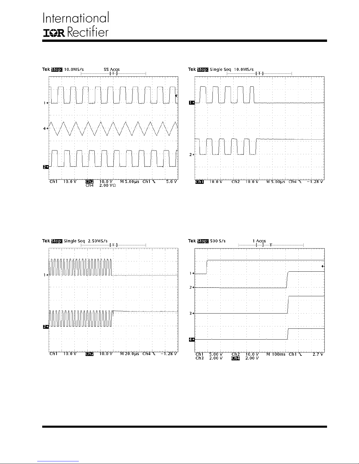
TYPICAL OPERATING CHARACTERISTICS
IRDC3073EVAL
Figure 1 - Normal condition at no load.
Ch1: HDrv
Ch2: LDrv
Ch4: Inductor Current
Figure 3 - Gate signals when SS pin pulls low.
Ch1: HDrv
Ch2: LDrv
Figure 2 - Gate signals when SS pin pulls low.
Ch1: HDrv
Ch2: LDrv
Rev. 1.0
06/30/03
www.irf.com
Figure 4 - Soft-Start.
Ch1: VIN (5V)
Ch2: Bias Voltage (12V)
Ch3: VOUT
Ch4: IOUT
7
Page 8
IRDC3073EVAL
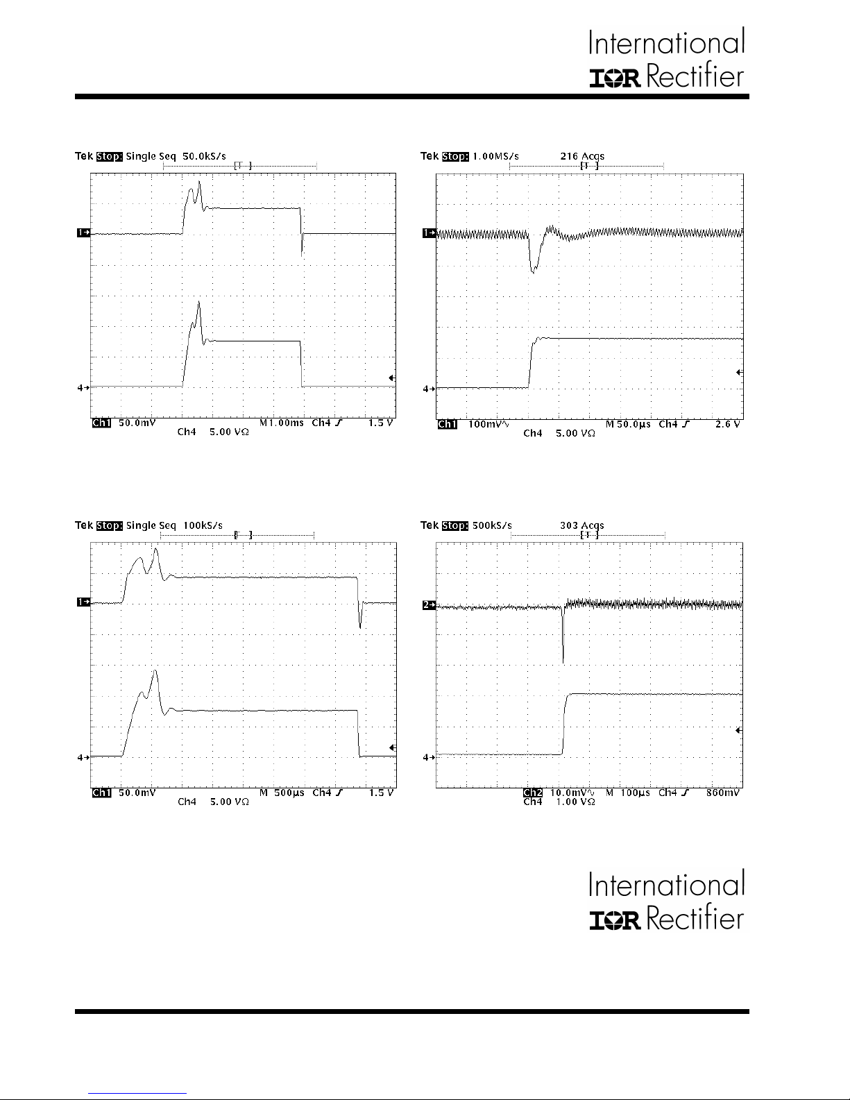
TYPICAL OPERATING CHARACTERISTICS
Figure 6 - Output Shorted at start-up.
Ch1: VOUT
Ch2: IOUT
Figure 7 - Output Shorted at start-up.
Ch1: VOUT
Ch2: IOUT
Figure 8 - Load Transient Response
(PWM Section).
Figure 10 - Load Transient Response
(PWM Section).
IR WORLD HEADQUARTERS: 233 Kansas St., El Segundo, California 90245, USA Tel: (310) 252-7105
8
TAC Fax: (310) 252-7903
Visit us at www.irf.com for sales contact information
Data and specifications subject to change without notice. 02/01
www.irf.com
Rev. 1.0
06/30/03
 Loading...