

Page 1
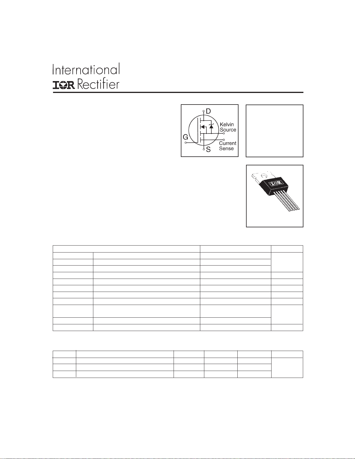
HEXFET® Power MOSFET
l Dynamic dv/dt Rating
l Current Sense
l 175°C Operating Temperature
l Fast Switching
l Ease of Paralleling
l Simple Drive Requirements
Description
Third Generation HEXFETs from International Rectifier provide the designer with
the best combination of fast switching, ruggedized device, low on-resistance and
cost-effectiveness.
The HEXSense device provides an accurate fraction of the drain current through
the additional two leads to be used for control or protection of the device. These
devices exhibit similar electrical and thermal characteristics as their IRF-series
equivalent part numbers. The provision of a kelvin source connection effectively
eliminates problems of common source inductance when the HEXSence is
used as a fast, high-current switch in non current-sensing applications.
PD - 9.529B
IRCZ44
V
= 60V
DSS
R
= 0.028Ω
DS(on)
ID = 50*A
TO-220 HexSense
Absolute Maximum Ratings
Parameter Max. Units
ID @ TC = 25°C Continuous Drain Current, VGS @ 10V 50*
ID @ TC = 100°C Continuous Drain Current, VGS @ 10V 37
I
DM
PD @TC = 25°C Power Dissipation 150 W
V
GS
E
AS
dv/dt Peak Diode Recovery dv/dt 4.5 V/ns
T
J
T
STG
Pulsed Drain Current 210
Linear Derating Factor 1.0 W/°C
Gate-to-Source Voltage ±20 V
Single Pulse Avalanche Energy 30 mJ
Operating Junction and -55 to + 175
Storage Temperature Range
Soldering Temperature, for 10 seconds 300 (1.6mm from case)
Mounting Torque, 6-32 or M3 screw 10 lbf•in (1.1 N•m)
Thermal Resistance
Parameter Min. Typ. Max. Units
R
θJC
R
θCS
R
θJA
Junction-to-Case — — 1.0
Case-to-Sink, Flat, Greased Surface — 0.50 —
Junction-to-Ambient — — — 62
°C/W
A
°C
C-13
Page 2
IRCZ44
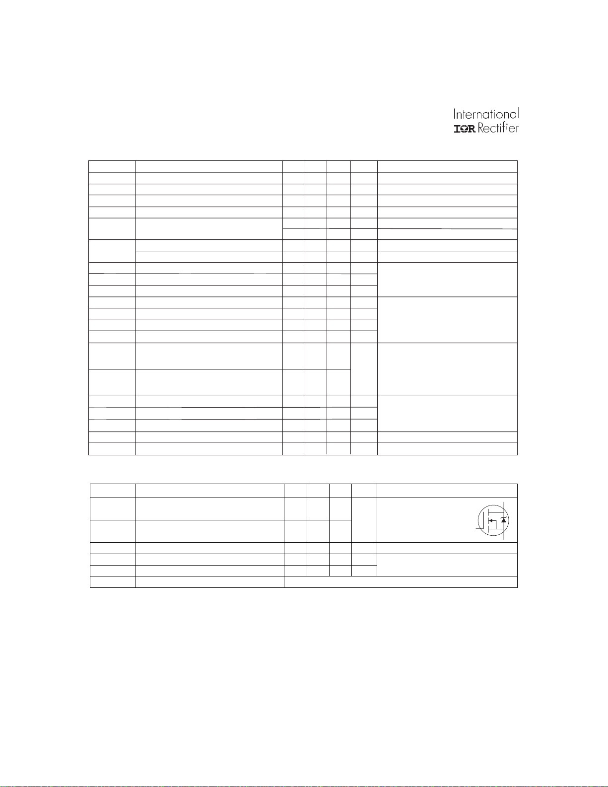
Electrical Characteristics @ TJ = 25°C (unless otherwise specified)
Parameter Min. Typ. Max. Units Conditions
V
(BR)DSS
∆V
(BR)DSS
R
DS(ON)
V
GS(th)
g
fs
DSS
I
GSS
Q
g
Q
gs
Q
gd
t
d(on)
t
r
t
d(off)
t
f
L
D
L
C
C
iss
C
oss
C
rss
r Current Sensing Ratio 2460 ––– 2720 ––– ID = 52A, VGS = 10V
C
oss
Drain-to-Source Breakdown Voltage 60 ––– ––– V VGS = 0V, ID = 250µA
/∆T
Breakdown Voltage Temp. Coefficient ––– 0.060 ––– V/°C Reference to 25°C, ID = 1mA
J
Static Drain-to-Source On-Resistance ––– ––– 0.028 Ω VGS = 10V, ID = 31A
Gate Threshold Voltage 2.0 ––– 4. 0 V VDS = VGS, ID = 250µA
Forward Transconductance 18 ––– ––– S VDS = 25V, ID = 31A
Drain-to-Source Leakage CurrentI
––– ––– 25 VDS = 60V, VGS = 0V
––– ––– 250 VDS = 48V, VGS = 0V, TJ = 150°C
Gate-to-Source Forward Leakage ––– ––– 100 VGS = 20V
Gate-to-Source Reverse Leakage ––– ––– -100 VGS = -20V
Total Gate Charge ––– ––– 95 ID = 52A
Gate-to-Source Charge ––– ––– 27 nC VDS = 48V
Gate-to-Drain ("Miller") Charge ––– ––– 4 6 VGS = 10V, See Fig. 6 and 13
Turn-On Delay Time ––– 19 ––– VDD = 30V
Rise Time ––– 120 ––– ID = 52A
Turn-Off Delay Time ––– 55 ––– RG = 9.1Ω
Fall Time ––– 86 ––– RD = 0.54Ω, See Fig. 10
Between lead,
Internal Drain Inductance ––– 4.5 –––
Internal Source Inductance ––– 7.5 – ––
nH
6 mm (0.25in.)
from package
and center of
die contact
Input Capacitance ––– 2500 ––– VGS = 0V
Output Capacitance ––– 1200 ––– pF VDS = 25V
Reverse Transfer Capacitance ––– 200 ––– ƒ = 1.0MHz, See Fig. 5
Output Capacitance of Sensing Cells ––– 9.0 –– – pF VGS = 0V, VDS = 25V, ƒ = 1.0MHz
Source-Drain Ratings and Characteristics
Parameter Min. Typ. Max. Units Conditions
I
S
I
SM
V
SD
t
rr
Q
rr
t
on
Notes:
Repetitive rating; pulse width limited by
max. junction temperature. ( See fig. 11 )
V
DD
R
G
C-14
Continuous Source Current MOSFET symbol
(Body Diode) showing the
Pulsed Source Current integral reverse
(Body Diode) p-n junction diode.
––– ––– 50*
––– ––– 210
Diode Forward Voltage ––– ––– 2.5 V TJ = 25°C, IS = 52A, VGS = 0V
Reverse Recovery Time ––– 140 300 ns TJ = 25°C, IF = 52A
Reverse Recovery Charge ––– 1.2 2. 8 nC di/dt = 100A/µs
Forward Turn-On Time
= 25V, starting TJ = 25°C, L = 0.013mH
= 25Ω, I
= 52A. (See Figure 12)
AS
Intrinsic turn-on time is negligible (turn-on is dominated by LS+LD)
I
≤ 52A, di/dt ≤ 250A/µs, V
SD
≤ 175°C
T
J
Pulse width ≤ 300µs; duty cycle ≤ 2%.
D
A
DD
≤ V
(BR)DSS
,
G
S
Page 3
IRCZ44
, Drain Current (Amps)
D
I
VDS, Drain-to-Source Voltage (Volts)
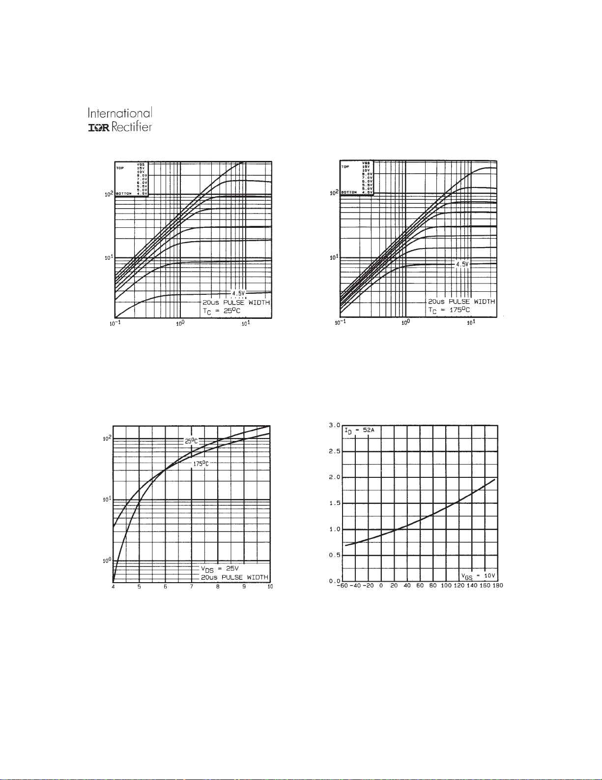
Fig. 1 Typical Output Characteristics,
TC=25°C
, Drain Current (Amps)
D
I
, Drain Current (Amps)
D
I
VDS, Drain-to-Source Voltage (Volts)
Fig. 2 Typical Output Characteristics,
TC=175°C
(Normalized)
, Drain to Source On-Resistance
DS(on)
VDS, Gate-to-Source Voltage (Volts)
R
TJ, Junction Temperature (°C)
Fig. 3 Typical Transfer Characteristics Fig. 4 Normalized On-Resistance vs.
Temperature
C-15
Page 4
IRCZ44
Capacitance (pF)
, Gate-to-Source Voltage (Volts)
GS
V
VDS, Drain-to-Source V oltage (V olts)
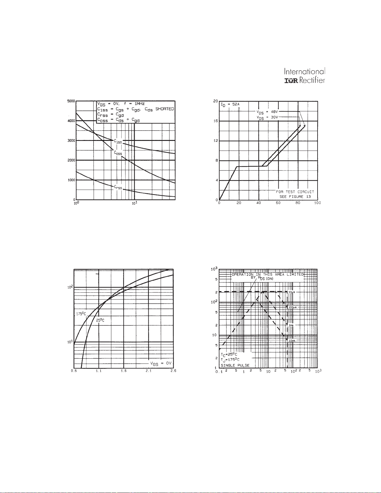
Fig. 5 Typical Capacitance vs. Drain-to-
Source V oltage
, Reverse Drain Current (Amps)
SD
I
VSD, Source-to-Drain V oltage (V olts)
Fig. 7 Typical Source-Drain Diode
Forward V oltage
QG, Total Gate Charge (nC)
Fig. 6 T ypical Gate Char ge vs. Gate-to-
Source V oltage
Drain Current (Amps)
D
I
VDS, Drain-to-Source Voltage (Volts)
Fig. 8 Maximum Safe Operating Area
C-16
Page 5
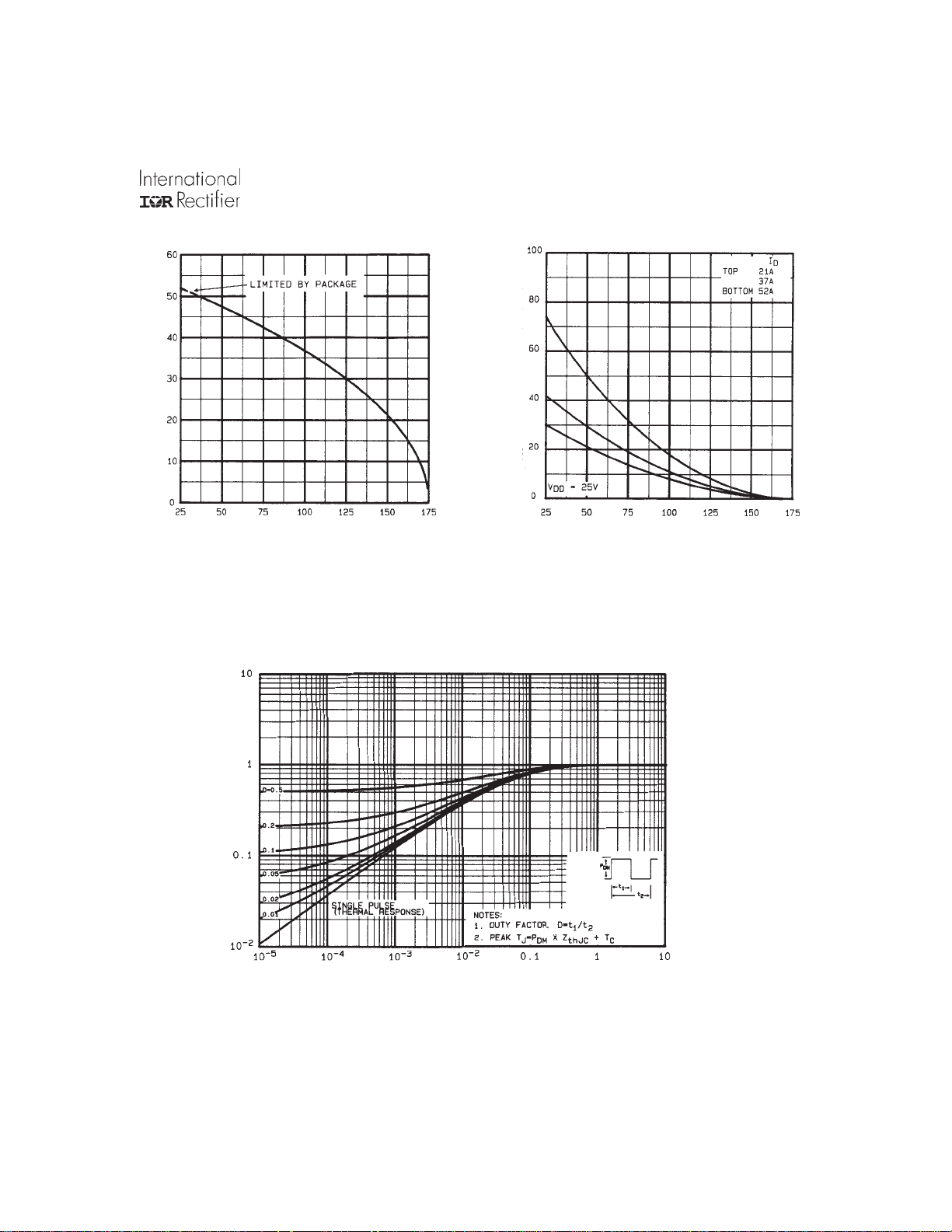
IRCZ44
, Drain Current (Amps)
D
I
TC, Case Temperature (°C)
Fig. 9 Maximum Drain Current vs.
Case Temperature
)
ΘJC
Thermal Repsonse (Z
, Drain Current (Amps)
D
I
Starting TJ, Junction Temperature (°C)
Fig. 12c Maximum Avalanche Energy
vs. Drain Current
t1, Rectiangular Pulse Duration (seconds)
Fig. 11 Maximum Effective Transient Thermal Impedance, Junction-to-Case
C-17
Page 6
IRCZ44
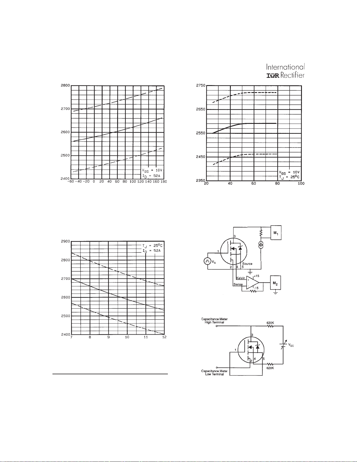
Sense Ratio (r)Sense Ratio (r)
TJ, Junction T emperature (°C)
Fig. 15 Typical HEXSense Ratio vs.
Junction Temperature
Sense Ratio (r)
ID, Drain Current (Amps)
Fig. 16 T ypical HEXSense Ratio vs.
Drain Current
Fig. 18 HEXSense Ratio Test Circuit
VGS, Gate-to-Source V oltage (Volts)
Fig. 17 Typical HEXSense Ratio vs.
Gate V oltage
Mechanical drawings, Appendix A
Part marking information, Appendix B
Test Circuit diagrams, Appendix C
C-18
Fig. 19 HEXSense Sensing Cell Output
Capacitance Test Circuit
 Loading...