

Page 1

In the absence of confirmation by device specification sheets, SHARP takes no responsibility for any defects that may occur in equipment using any SHARP devices shown in
catalogs, data books, etc. Contact SHARP in order to obtain the latest device specification sheets before using any SHARP device.
1
DESCRIPTION
The IR3Y38M is a bipolar single-chip signal
processing IC for CCD area sensors which includes
correlated double sampling circuit (CDS), clamp
circuit, automatic gain control amplifier (AGC),
reference voltage generator, black level detection
circuit, 10-bit analog-to-digital converter (ADC), and
serial interface for internal circuits.
FEATURES
• Low power consumption : 315 mW (TYP.)
• Wide AGC range : 12 to 43.5 dB
• High speed sample-and-hold circuits :
pulse width 12 ns (MIN.)
• Built-in standby mode for power saving
applications
• Built-in serial interface to control the AGC gain,
maximum gain and offset adjustment
• 10-bit ADC operating up to 18 MHz
• Digital interface for operating 3.3 V logic ICs
• Single +5 V power supply
• Package :
48-pin QFP (QFP048-P-0707) 0.5 mm pin-pitch
PIN CONNECTIONS
IR3Y38M
CCD Signal Process & Digital Interface IC
IR3Y38M
1
48 47 4645 44 4342 41 4039 37
13 14 1516 17 1819 20 2122 23 24
2
3
4
5
6
7
8
9
10
11
12
36
35
34
33
32
31
30
29
28
27
26
25
DO
0
DO1
DO2
DO3
DO4
GND6
VCC6
DO5
DO6
DO7
DO8
DO9
VCC2
Ô
OFSCTL
OBCAP
Î
fl/H
3
fl/H2
fl/H1
Â
‰
REFCAP
V
CC1
ADCK
GND
5
VCC5
SCK
V
CC4
GND4
SDATA
CLPCAP
CCDIN
REFIN
GND
1
SHISET
V
LOGIC
VRB
VRT
ÅNCADIN
ADOFS
AGCCTL
GND3AGCOUT
V
CC3
GND2
38
48-PIN QFP
TOP VIEW
(QFP048-P-0707)
Page 2
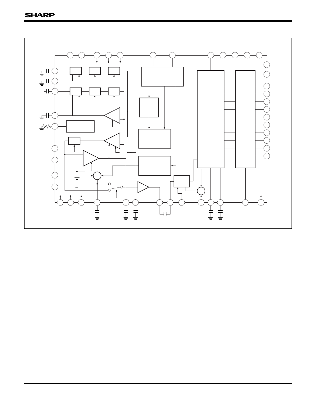
IR3Y38M
2
BLOCK DIAGRAM
CLAMP
6-BIT
OFFSET CONTROL
D/A CONVERTER
8-BIT
AGC GAIN CONTROL
D/A CONVERTER
MAX. GAIN
SELECTOR
SERIAL
PARALLEL
CONVERTER
25 23 28 29 30 16 19 13 17 18 15 14
V
CC1 GND1 Â fl/H1 SCK SDATA ADCK VCC4 GND4 VCC5 GND5fl/H2
7
6
12
11
10
9
8
5
4
3
2
1
V
CC6
GND6
DO9
DO8
DO7
DO6
DO5
DO4
DO3
DO2
DO1
DO0
2748464742454339413334353231
‰
V
LOGICVRTVRB
ADOFS
Å
ADIN
AGCOUTAGCCTL
OBCAP
OFSCTL
ÔÎfl/H3
40
38
37
36
24
20
21
26
22
GND
3
VCC3
GND2
VCC2
SHISET
CLPCAP
CCDIN
REFCAP
REFIN
CLAMP
S/H1 S/H2
CLP
fl/H
1
fl/H2
CLAMP
S/H1 S/H2
CLP
fl/H
1
OBP
OBP
BLK
fl/H
2
OUTPUT
BUFFER
BIAS ERROR
AMP
AGC
AMP
CLAMP & S/H
CURRENT SETUP
S/H3
fl/H3
BIAS GAIN
+
–
+
–
+
–
+
+
10-BIT
A/D
CONVERTER
Page 3

3
IR3Y38M
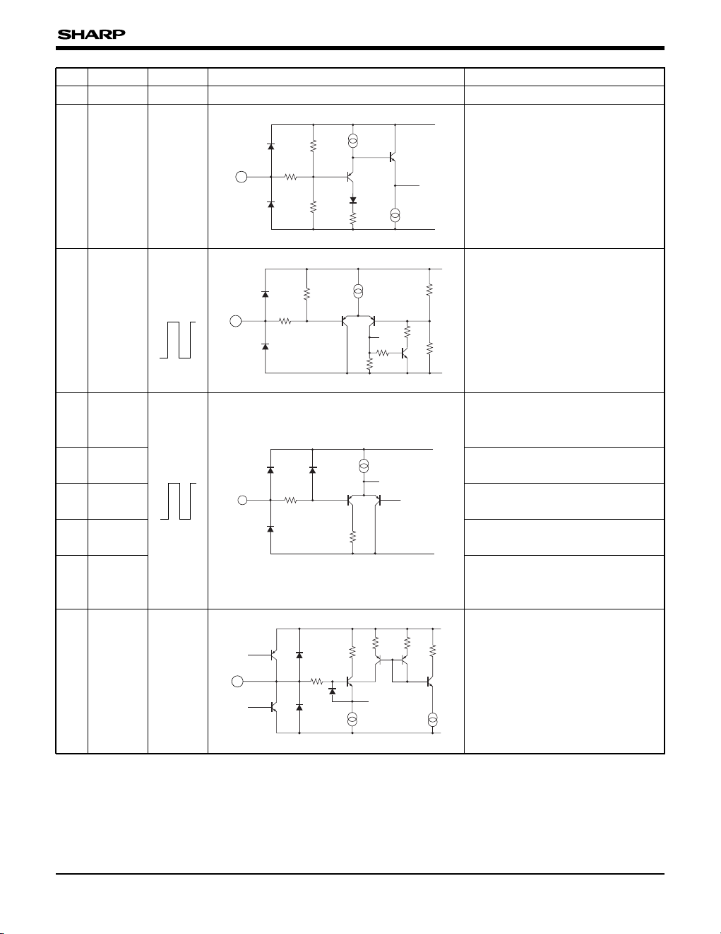
PIN DESCRIPTION
(The voltage is measured on condition that VCC1 to VCC6 = +5.0 V, VLOGIC = +3.3 V.)
1
DO
0
Digital data output pins of the A/D
converter. DO0 is LSB.
The data format is a straight binary
code.
V
OL : 0.2 V (TYP.)
V
OH : VLOGIC – 0.2 V (TYP.)
PIN NO.
PIN NAME VOLTAGE
EQUIVALENT CIRCUIT DESCRIPTION
200
VCC6
GND6
500
10 k
GND pin of the output buffer of the
A/D converter.
0.0 V
GND
6
6
7
V
CC6
5.0 V
200
VCC6
GND6
500
10 k
Digital data output pins of the A/D
converter. DO9 is MSB.
The data format is a straight binary
code.
V
OL : 0.2 V (TYP.)
VOH : VLOGIC – 0.2 V (TYP.)
DO
5
8
VCC5
200
150 µ
GND5
13
Clock input pin of the A/D
converter.
The A/D conversion is executed at
the rising edge of the ADCK, and
the data is output at the falling edge
of the ADCK.
Duty : 50%
fmax : 18 MHz (MIN.)
ADCK
13
DO
1
DO2
DO3
DO4
2
3
4
5
9
10
11
12
DO
6
DO7
DO8
DO9
14
GND
5
0.0 V
Digital GND pin of the A/D
converter.
Digital power supply pin of the A/D
converter.
5.0 V
V
CC5
15
Power supply pin of the output
buffer of the A/D converter.
16
SCK
Clock input pin of the serial
interface.
Refer to "TRUTH TABLE" of pin 19.
VCC1
200
15 µ
GND1
16
3.1 V
0.2 V
3.1 V
0.2 V
> 2.1 V
< 0.7 V
> 2.1 V
< 0.7 V
Page 4

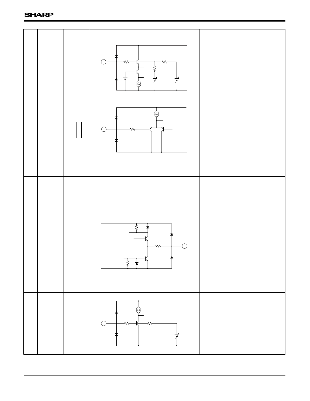
IR3Y38M
4
17
V
CC4
5.0 V
Analog power supply pin of the A/D
converter.
PIN NO.
PIN NAME VOLTAGE EQUIVALENT CIRCUIT DESCRIPTION
Analog GND pin of the A/D
converter.
0.0 V
GND
4
18
19
SDATA
Data input pin of the serial
interface.
TRUTH TABLE
VCC1
200
15 µ
GND1
19
VCC1
200
100 µ
GND1
20
Bias decoupling pin of the CDS
signal clamp circuit. This pin is
connected to the GND
1 via a
capacitor.
3.2 V
CLPCAP
20
SDATA
1
0
DATA SHIFT
–
STORE
Action
›
fi
fi
SCK
23
GND
1
0.0 V
GND pin of the CDS/AGC.
Pay careful attention to board
layout of the GND
1 because the
CDS/AGC are noise-sensitive
circuitry.
21
CCDIN
2.5 V
Signal input pin of the CDS.
Input CCD signal to this pin via a
capacitor.
26 k
26 k
VCC1
200
150 µ
150 µ
GND1
2.5 V
REFIN
22
Reference input pin of the CDS.
This pin is connected to the GND
1
via a capacitor.
13 k
200
2 k
2 k
26 k
VCC1
GND1
24
Operation current setting pin of the
CDS and fl/H3 circuits.
This pin is connected to the GND
1
via a resistor.
The slew rates of the fl/Hs are in
inverse proportion to the value of
the resistor.
1.7 V
SHISET
24
> 2.1 V
< 0.7 V
Page 5
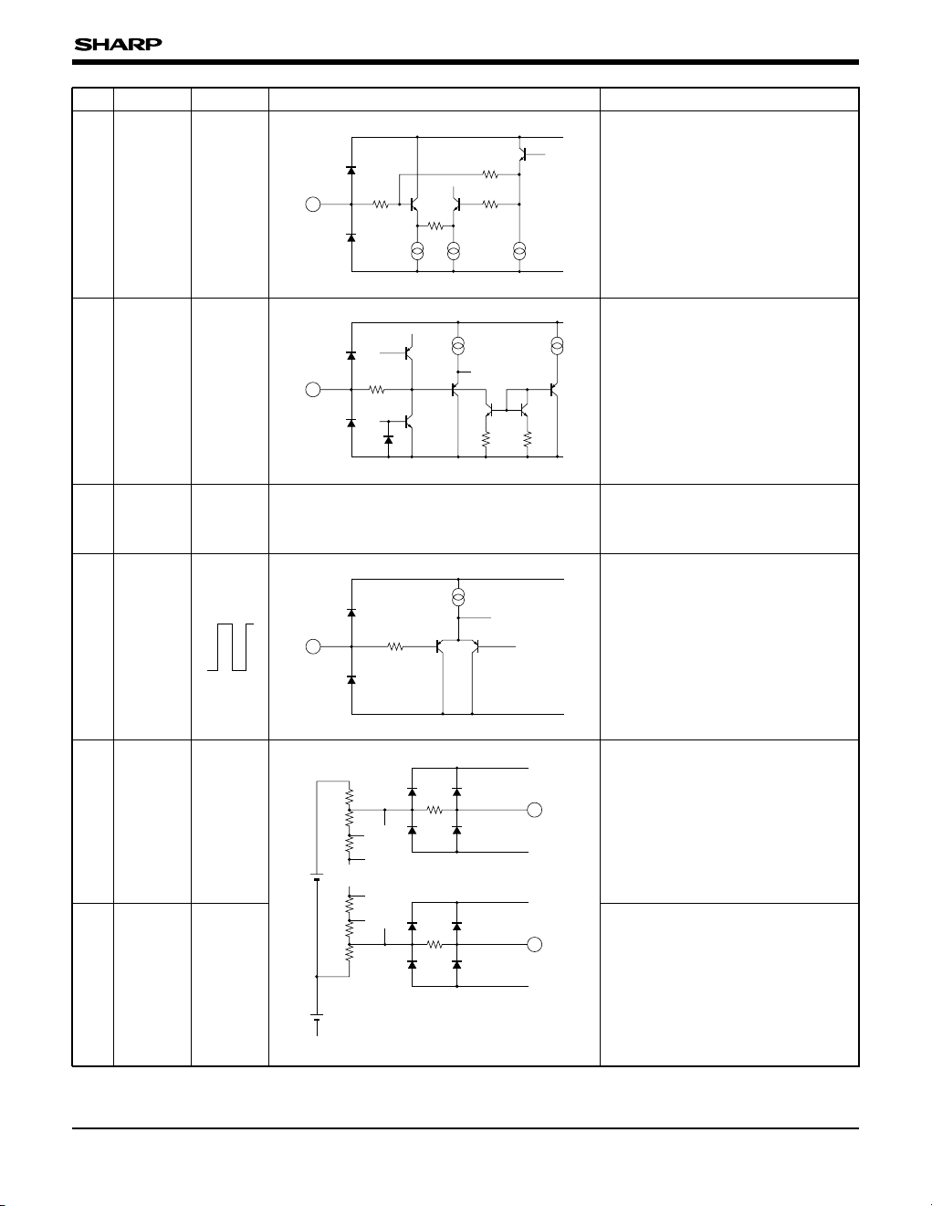
IR3Y38M
5
25
V
CC1 5.0 V
Power supply pin of the CDS/AGC.
PIN NO.
PIN NAME VOLTAGE
EQUIVALENT CIRCUIT DESCRIPTION
200
63 k
36 k
2 k
150 µ
75 µ
VCC1
GND1
26
Bias decoupling pin of the CDS
reference clamp circuit.
This pin is connected to the GND
1
via a capacitor.
3.2 VREFCAP
26
27
‰
Standby function control pin. All
actions stop and the power
consumption is decreased when
low.
The threshold voltage has 0.4 V
hysteresis.
Connect to the Vcc if not used.
68 k
75 k
65 k
32 k
110 k
VCC1
200
10 k
40 µ
GND1
27
VCC2
200
80 µ
GND2
20 k
3.3 k
20 k
3.3 k
80 µ
33
Clamp capacitor pin of the optical
black clamp (OPB clamp) circuit.
Connect to the GND
2 via a
capacitor.
3.7 VOBCAP
33
100
VCC1
200
50 µ
GND1
Pulse input pin of the CDS feedthrough level clamp.
Signal is clamped when low.
Â
28
29
30
31
32
fl/H
1
fl/H2
flH3
Î
Pulse input pin of the OPB clamp
and bias error amplifier.
Signal is clamped when low.
Pulse input pin of the fl/H
3.
Signal is sampled when low.
Pulse input pin of the fl/H
2.
Signal is sampled when low.
Pulse input pin of the fl/H
1.
Signal is sampled when low.
> 2.1 V
< 0.7 V
5.0 V
(open)
> 2.1 V
< 0.7 V
Page 6
IR3Y38M
6
34
OFSCTL
2.15
to
2.30 V
Decoupling capacitor pin of the
blanking offset control D/A
converter. Connect to the GND
1 via
a capacitor.
PIN NO.
PIN NAME VOLTAGE
EQUIVALENT CIRCUIT DESCRIPTION
VCC1
200 30 k
100 µ
GND1
D/A2.2 V
10 k
34
VCC2
200
20 µ
GND2
35
VCC3
GND3
20
300
10 k
39
Blanking pulse input pin.
The output of the AGCOUT pin is
blanked when low. The blanking
level can be controlled by the serial
interface.
Ô
35
36
V
CC2 5.0 V
Power supply pin of the fl/H
3 and
OPB clamp circuits.
GND pin of the fl/H
3 and OPB
clamp circuits.
0.0 VGND
2
37
38
V
CC3 5.0 V
Power supply pin of the output
buffer circuit connected to the
AGCOUT pin.
Signal output pin of the AGC.
Connect to the ADIN pin via a
capacitor.
0.9 V
(Î = L)
AGCOUT
39
VCC1
200 11 k
50 µ
GND1
D/A
41
Decoupling capacitor pin of the
AGC gain control D/A converter.
Connect to the GND
1 via a
capacitor.
2.5
to
3.8 V
AGCCTL
41
40
GND
3 0.0 V
GND pin of the output buffer circuit
connected to the AGCOUT pin.
> 2.1 V
< 0.7 V
Page 7
IR3Y38M
7
42
ADOFS
3.3 V
(open)
Input range
1.6
to
5.0 V
Voltage adjustment pin of the ADC
black level clamp. This pin is biased
at 3.3 V from the inside of the IC.
Connect to the GND
4 via a
capacitor if not used.
PIN NO.
PIN NAME VOLTAGE
EQUIVALENT CIRCUIT DESCRIPTION
VCC4
200 70 k
25 µ 75 µ25 µ
GND4
70 k
79 k
42
50 µ50 µ
VCC4
200
GND4
16 k
16 k
43
Signal input pin of the ADC.
Connect to the AGCOUT pin via a
capacitor.
This capacitor is also used as the
clamp capacitor of the ADC blank
level clamp.
1.4 V
(Å = L)
ADIN
43
25 µ
VCC4
200
GND4
45
> 2.1 V
< 0.7 V
Pulse input pin of the ADC black
level clamp. Signal is clamped
when low.
When the ADOFS is opened, the
clamped level is set to make the
ADC output 61 (decimal).
Å
45
44
NC
No connection. It is recommended
to connect to GND for better heat
radiation and avoiding noise.
46
V
RT 3.90 V
Upper reference decoupling pin of
the ADC. Connect to the GND
4 via
a capacitor.
VCC4
VRT
GND4
5
VCC4
VRB
GND4
GND4
5
47
46
Lower reference decoupling pin of
the ADC. Connect to the GND
4 via
a capacitor.
1.95 VV
RB
47
Page 8

IR3Y38M
8
FUNCTIONAL DESCRIPTION
CDS Circuit
The clamp circuit clamps the feed-through level of
the CCD signal with the  pulse. Then the fl/H
1
circuit samples the signal period of the one with the
fl/H
1 pulse and holds on. Thus the video signal is
obtained. But this signal has a level drop caused by
the reset pulse of the CCD signal, and for removing
it, the fl/H
2 circuit samples this signal again with the
fl/H
2 pulse.
For reducing the effect of the sampling pulse or
other noise sources, the CDS circuit is formed with
a differential structure.
Bias Error Amplifier Circuit
For stabilizing the bias level of the CDS circuit and
reducing the offset of the AGC circuit, the bias error
amplifier acts with the Î pulse during the OPB
period.
AGC Amplifier Circuit
The AGC amplifier amplifies the video signal
obtained by the CDS circuit. The gain of the AGC
is controlled by the value of the AGCGAIN serial
register. And the maximum gain of the AGC is
controlled by the value of the GAINSEL serial
register.
OPB Clamp Circuit
For clamping the level of the amplified signal to the
black level, the OPB clamp circuit acts with the
Î pulse during the OPB period.
Blanking Circuit
The output signal is fixed to the blanking level with
the Ô pulse. The blanking level is the sum of the
black level and the offset value decided by the
value of the OFFSET serial register.
A/D Converter Circuit
The fl/H3 circuit samples the amplified signal with
the fl/H
3 pulse and the A/D converter converts the
sampled signal to 10-bit straight binary digital data.
The clamp circuit placed in front of the A/D
converter clamps the signal level beside the lower
limit of the convertible input range with the Å
pulse. The clamped level is controllable by the
voltage of the ADOFS pin.
The A/D conversion is executed at the rising edge
of the ADCK clock, and the data is output at the
falling edge.
The high level voltage of the outputs is controlled
by the voltage of the V
LOGIC pin.
Standby Function
By making the ‰ pin low, all actions of this IC
stop and power consumption is decreased.
The outputs of the A/D converter (DO
0 to DO9) turn
to high impedance when on standby.
PIN NO.
PIN NAME VOLTAGE
EQUIVALENT CIRCUIT DESCRIPTION
48
V
LOGIC 3.3 V
ADC output voltage setting pin. The
high level voltage of the DO
0 to
DO9 pins is set to VLOGIC – 0.2 V.
It is recommended to connect to the
power supply of the following logic
ICs.
25 µ
VCC5
200
GND5
48
Page 9

Serial Interface Circuit
The IR3Y38M has a serial interface to control the
gain of the AGC amplifier and the offset of the
blanking level. This interface is constituted by a shift
register for serial-parallel conversion, data registers
and D/A converters.
The data input to SDATA is fetched and shifted at
the rising edge of the SCK. While transmitting data,
the SDATA must be low when the SCK falls. When
the SDATA is high and the SCK falls, the data on
the shift register is stored at the selected data
register at the following falling edge of the SDATA.
The stored data register is selected by the data of
the D
0 and D1 bits.
IR3Y38M
9
D0
D1
D2-D9
SDATA
SCK
Shift Register Decoder
Select
Store
3-bit
Register
8-bit
Register
6-bit
Register
Gain
Selector
8-bit
D/A Converter
6-bit
D/A Converter
AGC GAIN OFFSET
D9 D8 D7
D6 D5 D4
D3 D2 D1
D0
3.3 µs min.
Dummy
Cycle
SCK
SDATA
Store
GAIN SEL = 7
GAIN SEL = 0
2550
12
22
43.5
AGC GAIN (dB)
Value of AGC GAIN
630
–75
65
OFFSET (mV)
Value of OFFSET
GAIN SEL
0
1
2
3
4
5
6
7
MAXIMUM GAIN (dB)
22
25
28
31.5
34.5
38
41
43.5
DATA REGISTER
(Don't care)
OFFSET
AGC GAIN
GAIN SEL
d
0
D9 D0
1
0
1
0
D
1
1
1
0
0
D
2
d5
d7
d2
D3
d4
d6
d1
D4
d3
d5
d0
D5
d2
d4
D6
d1
d3
D7
d0
d2
D8
d1
LSB MSB
Page 10

IR3Y38M
10
TIMING CHART
SIG1
SIG2
SIG3
Signal
Level
Reset
Pulse
Feed-through
Level
CCD
IN
Â
fl/H
1
S/H1
output
S/H
2
output
AGC
output
S/H
3
output
fl/H
2
fl/H3
ADCK
DO
0-DO9
tDLH
tDHL
tWLH
tWHL
SIG1
SIG2
SIG2 SIG3
SIG1
SIG3
SIG1
SIG3
SIG2
SIG1
SIG2
SIG3
SIG1
SIG2
SIG3
Page 11

IR3Y38M
11
–1 ns min.
2 ns min.
12 ns min.
3 ns min.
2 ns min.
5 ns min. 3 ns min.12 ns min.
12 ns min.35 ns min.
35 ns min. 1 ns min. 12 ns min.
25 ns min.25 ns min.
3 ns min.
signal interval signal intervalOPB interval
idle transfer
interval
1.5 µs min.
1.5 µs min.
CCD
IN
Â
fl/H
1
fl/H2
fl/H3
ADCK
Î
Ô
Å
Page 12

PRECAUTIONS
Each VCC1 to VCC6 pin corresponds to the each
GND
1 to GND6 pin. Connect a ceramic capacitor
as near the IC as possible between each
corresponding V
CC pin and GND pin.
The GND
1 pin is the ground of the CDS/ADC
circuit handling a weak signal. Pay careful attention
to the board layout of the GND
1 pattern in order to
avoid the potential fluctuation of the GND
1 caused
by the current of the other GND pins. Especially
pay attention to the current of the GND
6 pin's
flowing spiky current.
All the GND pins must be at the same potential
and not open. And keep the potential difference of
each V
CC pin within 0.3 V.
The high level voltage of the outputs of the A/D
converter is controllable by the voltage of the
V
LOGIC pin, but take care that the high level voltage
does not fall below about 1.5 V, in spite of making
the V
LOGIC pin 0 V. This may cause the latch up of
the following logic ICs if the power supply of this IC
rises up faster than the power supply of the
following logic. To avoid this problem, it is
recommended to make the ‰ pin low until the
voltage of the logic power supply becomes stable.
Take care too that the high level voltage does not
rise above about V
CC – 1.0 V, in spite of making
the V
LOGIC pin the VCC potential.
Restore the value of the serial register when setting
up the power supply or making the ‰ pin high
because the value will have been removed in that
case.
IR3Y38M
12
ABSOLUTE MAXIMUM RATINGS (Unless otherwise specified, TA = +25 ˚C)
PARAMETER SYMBOL CONDITIONS UNIT
Supply voltage V
CC1-VCC6 V7
RATING
VIN –0.3 to VCC + 0.3 V
mW/˚C4.5T
A > +25 ˚C
570 mWT
A ≤ +25 ˚CPD
Input voltage
P
D derating ratio
TOPR ˚C–30 to +70
–55 to +150 ˚CT
STG
Operating temperature
Storage temperature
Power consumption
RECOMMENDED OPERATING CONDITIONS
PARAMETER SYMBOL APPLICABLE PINS UNIT
Supply voltage V
CC1-VCC6 V4.75 to 5.25
RATING
Standard CCD input signal level V
CCD CCDIN mVp-p200
2.1 to V
CC
V
‡, SCK, SDATA,
‰, Â, fl/H
1, fl/H2,
fl/H3, Î, Ô, Å
V
IHInput "High" voltage
0 to 0.7
V
V
ILInput "Low" voltage
≥ 12 nsÂ, fl/H
1, fl/H2, fl/H3tWS/HS/H pulse width
Serial interface clock frequency f
SCK SCK kHz≤ 300
A/D converter clock frequency f
ADCK ADCK MHz≤ 18
Clamp pulse width tWC Î, Å µs≥ 1.5
Page 13

13
Input "High" current
(4)
I
IH4
Apply to pin 13 (ADCK).
VIH = 3.3 V
0–µA0.1
Input "High" current
(3)
I
IH3
Apply to pin 35 (Ô) and pin 45 (Å).
V
IH = 3.3 V
0–µA0.1
Input "High" current
(2)
I
IH2
Apply to pin 16 (SCK) and pin 19 (SDATA).
V
IH = 3.3 V
0–µA0.1
Input "High" current
(1)
I
IH1
Apply to pin 28 (Â), pin 29 (fl/H1), pin 30
(fl/H2), pin 31 (fl/H3), and pin 32 (Î).
V
IH = 3.3 V
0–µA0.1
IR3Y38M
ELECTRICAL CHARACTERISTICS
DC Characteristics
(Unless otherwise specified, TA = +25 ˚C, VCC1 = VCC2 = VCC3 = VCC4 = VCC5 = VCC6 = 5.0 V, VLOGIC = 3.3 V,
ADCK = 0 V, SCK = 0 V, SDATA = 0 V, ‰ = 3.3 V, Â = 0 V, fl/H
1 = 0 V, fl/H2 = 0 V, fl/H3 = 0 V,
Ô = 3.3 V, Î = 0 V, SW42 = OFF, SW43 = (a), Å = 3.3 V)
The current direction flowing into the pin is positive direction.
PARAMETER SYMBOL CONDITIONS TYP.
Supply current (1) I
CC1 Measure pin 25 (VCC1)27–
MIN.
mA
UNIT
34
MAX.
1.0 mA– 0.7Measure pin 38 (V
CC3).ICC3
2.8 mA– 2.3Measure pin 36 (VCC2).ICC2
• General
Supply current (2)
Supply current (3)
Total supply current I
CC Total of ICC1 to ICC6 63–mA77
Supply current (6) ICC6 Measure pin 7 (VCC6). 5.0–mA6.5
Supply current (5) I
CC5 Measure pin 15 (VCC5). 16–mA21
Supply current (4) ICC4 Measure pin 17 (VCC4). 13–mA20
6.5 mA– 4.5‰ = 0 V, Total of I
CC1 to ICC6.ISTBY
Standby supply
current
Input "Low" current
(1)
I
IL1
Apply to pin 28 (Â), pin 29 (fl/H1), pin 30
(fl/H2), pin 31 (fl/H3), and pin 32 (Î).
V
IL = 0 V
–2.0–3.5 µA–
–µA–0.3 –0.2
Apply to pin 16 (SCK) and pin 19 (SDATA).
V
IL = 0 V
I
IL2
Input "Low" current
(2)
Input "Low" current
(3)
I
IL3
Apply to pin 35 (Ô) and pin 45 (Å).
V
IL = 0 V
–0.3–0.5 µA0
–V4.5 5.0Open pin 27 (‰).V
27‰ voltage
‰ impedance Z27 11070 k$140
–µA–3.5 –2.0
Apply to pin 13 (ADCK).
V
IL = 0 V
I
IL4
Input "Low" current
(4)
Page 14

14
IR3Y38M
AGCOUT voltage V39 0.90.7 V1.1
OBCAP voltage V
33 3.73.3 V4.0
REFCAP voltage V26 3.22.9 V3.6
–110 µA– –135
CLPCAP = 2.8 V, OBP = 0 V
Measure the current of CLPCAP.
I
L20
CLPCAP charge
current
15 k$711Z41AGCCTL impedance
12 k$69Z
34OFSCTL impedance
32 k$15 23Z26REFCAP impedance
18 k$913Z
22REFIN impedance
18 k$913Z
21CCDIN impedance
OBCAP leakage
current
I
Z33
OBCAP = 3.7 V, OBP = 3.3 V
Measure the current of OBCAP.
0–0.5 µA0.5
OBCAP discharge
current
I
H33
OBCAP = 4.1 V, OBP = 0 V
Measure the current of OBCAP.
9065 µA–
OBCAP charge
current
I
L33
OBCAP = 3.3 V, OBP = 0 V
Measure the current of OBCAP.
–90–µA–65
CLPCAP leakage
current
I
Z20
CLPCAP = 3.2 V, OBP = 3.3 V
Measure the current of CLPCAP.
0–0.5 µA0.5
CLPCAP discharge
current
I
H20
CLPCAP = 3.6 V, OBP = 0 V
Measure the current of CLPCAP.
135110 µA–
2.8 V2.3 2.5V
22REFIN voltage
SHISET voltage V
24 1.71.5 V1.9
PARAMETER SYMBOL CONDITIONS TYP.
CLPCAP voltage V
20 3.22.9
MIN.
V
UNIT
3.6
MAX.
2.8 V2.3 2.5V
21
• CDS & AGC Circuits
CCDIN voltage
Page 15

IR3Y38M
15
• A/D Converter Circuit
PARAMETER SYMBOL CONDITIONS TYP.MIN. UNITMAX.
ADOFS voltage V
42 3.33.0 V3.6
4.1 V3.7 3.9V
46
1.6 V1.2 1.4ADCLP = 0 VV43ADIN voltage
VRT voltage
ADOFS impedance Z
42 7050 k$90
V
RB voltage V47 1.951.8 V2.2
–30 45
ADIN = 1.8 V, ADCLP = 0 V
Measure the current of ADIN.
I
H43
ADIN discharge
current
µA
ADIN charge current I
L43
ADIN = 1.0 V, ADCLP = 0 V
Measure the current of ADIN.
–45–µA–30
0.3–0.3 0
ADIN = 1.4 V, ADCLP = 3.3 V
Measure the current of ADIN.
I
Z43ADIN leakage current µA
V0.4– 0.2
SW43 = (b), ADCIN = 0.8 V
Change the level of ADCK to L
/H/L, then
measure the voltages of DO
0 to DO9 pins.
V
OLOutput "Low" voltage
Output "High" voltage V
OH
SW43 = (b), ADCIN = 3.5 V
Change the level of ADCK to L/H/L, then
measure the voltages of DO
0 to DO9 pins.
3.12.9 – V
Page 16

IR3Y38M
16
AC Characteristics
(Unless otherwise specified, TA = +25 ˚C, VCC1 = VCC2 = VCC3 = VCC4 = VCC5 = VCC6 = 5.0 V, VLOGIC = 3.3 V,
ADCK = 0 V, SCK = 0 V, SDATA = 0 V, ‰ = 3.3 V, Â = 3.3 V, fl/H
1 = 0 V, fl/H2 = 0 V, fl/H3 = 0 V,
Ô = 3.3 V, Î = 3.3 V, SW42 = OFF, SW43 = (a), Å = 3.3 V, (OFFSET) = 32)
The value of the serial register is written with decimal.
PARAMETER SYMBOL CONDITIONS TYP.
AGC minimum gain G
AN
(GAIN SEL) = 0, (AGC GAIN) = 0
 = SG2, Π= SG3
Input the attenuated SG1 (f = 2 MHz, V = 1.6
Vp-p) to the SIN and seek the attenuation
amount to make the amplitude of AGCOUT
1.6 Vp-p.
1211
MIN.
dB
UNIT
13
MAX.
• CDS & AGC Circuits
24.5 dB20.5 22
(GAIN SEL) = 0, (AGC GAIN) = 255
Measure the gain using the same procedure
as for the measurement of GAN.
GAX0
AGC maximum gain
(0)
AGC maximum gain
(4)
G
AX4
(GAIN SEL) = 4, (AGC GAIN) = 255
Measure the gain using the same procedure
as for the measurement of G
AN.
34.531 dB38
AGC maximum gain
(3)
G
AX3
(GAIN SEL) = 3, (AGC GAIN) = 255
Measure the gain using the same procedure
as for the measurement of G
AN.
31.528.5 dB35
AGC maximum gain
(2)
G
AX2
(GAIN SEL) = 2, (AGC GAIN) = 255
Measure the gain using the same procedure
as for the measurement of G
AN.
2826 dB31
AGC maximum gain
(1)
G
AX1
(GAIN SEL) = 1, (AGC GAIN) = 255
Measure the gain using the same procedure
as for the measurement of G
AN.
2523 dB28
AGC maximum gain
(5)
G
AX5
(GAIN SEL) = 5, (AGC GAIN) = 255
Measure the gain using the same procedure
as for the measurement of G
AN.
3834 dB42
AGC gain variable
width
G
AR GAR = GAX7 – GAN 31.526.5 dB35.5
AGC maximum gain
(7)
G
AX7
(GAIN SEL) = 7, (AGC GAIN) = 255
Measure the gain using the same procedure
as for the measurement of G
AN.
43.538.5 dB47.5
AGC maximum gain
(6)
G
AX6
(GAIN SEL) = 6, (AGC GAIN) = 255
Measure the gain using the same procedure
as for the measurement of G
AN.
4136.5 dB44.5
Page 17

IR3Y38M
17
Output dynamic
range (2)
(Maximum gain)
VDYX
(GAIN SEL) = 7, (AGC GAIN) = 255
 = SG2, Π= SG3
Input the SG1 (f = 2 MHz, V = 50 mVp-p) to the
SIN and measure the amplitude of the AGCOUT.
2.22.0 Vp-p–
PARAMETER SYMBOL CONDITIONS TYP.MIN. UNITMAX.
Bandwidth (1)
(Minimum gain)
f
TN
(GAIN SEL) = 0, (AGC GAIN) = 0
 = SG2, Π= SG3
Input the SG1 (f = 2 MHz, V = 0.2 Vp-p) to
the SIN and measure the amplitude of the
AGCOUT. Increase the frequency and
measure the frequency when the amplitude
attenuates to –3 dB.
3524 MHz–
– MHz13 20
(GAIN SEL) = 7, (AGC GAIN) = 255
 = SG2, Π= SG3
Input the SG1 (f = 2 MHz, V = 8 mVp-p) to
the SIN and measure the amplitude of the
AGCOUT. Increase the frequency and
measure the frequency when the amplitude
attenuates to –3 dB.
f
TX
Bandwidth (2)
(Maximum gain)
OFFSET adjustment
limit (2)
(OFFSET = 63)
V
BOX
(GAIN SEL) = 0, (AGC GAIN) = 0
SIN = GND
1, (OFFSET) = 63, Â = 0 V,
Î = 0 V
Measure the V
BO21 and VBO22 similarly to
above-mentioned method.
V
BON = VBO22 – VBO21
6550 mV–
OFFSET adjustment
limit (1)
(OFFSET = 0)
V
BON
(GAIN SEL) = 0, (AGC GAIN) = 0
SIN = GND1, (OFFSET) = 0, Â = 0 V,
Î = 0 V
Measure the voltage of the AGCOUT at BLK
= 3.3 V and define it V
BO11.
Measure the one similarly at BLK = 0 V and
define it V
BO12.
V
BON = VBO12 – VBO11
–75–mV–60
– Vp-p2.0 2.2
(GAIN SEL) = 0, (AGC GAIN) = 0
 = SG2, Π= SG3
Input the SG1 (f = 2 MHz, V = 0.9 Vp-p) to the
SIN and measure the amplitude of the
AGCOUT.
V
DYN
Output dynamic
range (1)
(Minimum gain)
Page 18

IR3Y38M
18
• A/D Converter Circuit
(Unless otherwise specified, T
A = +25 ˚C, VCC1 = VCC2 = VCC3 = VCC4 = VCC5 = VCC6 = 5.0 V, VLOGIC = 3.3 V,
ADCK = 18 MHz square wave, ˘= 0 V, ˙ = 0 V, ‰ = 3.3 V, Â = 3.3 V, fl/H
1 = 0 V, fl/H2 = 0 V,
fl/H
3 = 0 V, Ô = 3.3 V, Î = 3.3 V, SW42 = OFF, SW43 = (b), Å = 3.3 V)
PARAMETER SYMBOL CONDITIONS TYP.
Clamp value D
CLP
SW43 = (a)
Å = 0 V
ADCIN = GND
4
Read the output value of DO0 to DO9.
6156
MIN.
–
UNIT
66
MAX.
41 –31 36
SW42 = ON, V
42 = 5.0 V, Å = 0 V,
ADCIN = GND
4
Read the output value of DO0 to DO9.
DCLPN
Clamp value
adjustment limit (1)
Differential linearity
error
DLE
ADCIN = SG4
Read the output value of DO
0 to DO9 at about
10
6
times and make it a histogram. Normalize
the histogram and obtain the DLE.
Integrate the histogram and obtain the ILE.
±0.5– LSB±0.9
Clamp value
adjustment limit (2)
D
CLPX
SW42 = ON, V42 = 1.6 V, Å = 0 V,
ADCIN = GND4
Read the output value of DO0 to DO9.
8681 –91
Propagation delay
(L/H)
t
DLH
ADCIN = SG4, CL = 20 pF
Measure the delay time from the falling edge
(50%) of the ADCK to the rising edge (50%)
of the DO
0 to DO9.
2615 ns38
ILEIntegral linearity error ±7 LSB–±3
25 ns10 17
ADCIN = SG4, C
L = 20 pF
Measure the fall time (90%/10%) of the
DO
0 to DO9.
tWHLOutput fall time
25 ns10 17
ADCIN = SG4, C
L = 20 pF
Measure the rise time (10%/90%) of the
DO
0 to DO9.
tWLHOutput rise time
38 ns15 26
ADCIN = SG4, C
L = 20 pF
Measure the delay time from the falling edge
(50%) of the ADCK to the falling edge (50%)
of the DO
0 to DO9.
tDHL
Propagation delay
(H/L)
Page 19

IR3Y38M
19
Measurement Waveforms
f [Hz]
V
3.3 V
0 V
3.3 V
0 V
3.5 V
1.1 V
1 ms
below 100 µs
above 1.5 µs
SG1
SG2
SG3
SG4
Page 20

IR3Y38M
20
Test Circuit
AGCOUT
ADIN
Å
Ô
36 35 34 33 32 31 30 29 28 27 26 25
123456789101112
24
23
22
21
20
19
18
17
16
15
14
13
37
38
39
40
41
42
43
44
45
46
47
48
Î fl/H3 fl/H2 fl/H1 Â
0.1 µF0.1 µF
Vcc
2
Vcc2
Vcc3
GND2
Vcc3
GND3
NC
V
RT
VRB
VLOGIC
AGC
ERR
S/H
3
0.1 µF
0.1 µF
SW43
SW42
v42
(a)
0.1 µF
0.1 µF
100 µF 0.1 µF
0.1 µF100 µF
V27
STBY
SHISET
GND
1
GND5
Vcc4
Vcc5
Output Buffer
10-bit A/D Converter
Serial/Parallel
Converter
Gain
Selector
CLAMP
6-bit
D/A
8-bit
D/A
Gain
Bias
+
+
+–
+
–
+
–
S/H
2
S/H2
S/H1
S/H1
Clamp
Clamp
Vcc6
GND6
0.1 µF
100 µF
0.1 µF
0.1 µF
1 µF
1 µF
100 µF
0.1 µF
0.1 µF
100 µF
V
CC5
VCC4
ADCK
SCK
SDATA
SIN
GND
22 K$
Vcc
1
DO9DO8DO7DO6DO5
DO4DO3DO2DO1DO0
Vcc6
0.1 µF
100 µF
Vcc
1
GND4
20 pF
20 pF
20 pF
20 pF
20 pF
20 pF
20 pF
20 pF
20 pF
20 pF
(b)
+
+
+
+
+
+
Page 21

PACKAGES FOR CCD AND CMOS DEVICES
21
36
25
37
48
121
0.15
±0.05
0.1
±0.1
9.0
±0.3
7.0
±0.2
7.0
±0.2
(1.0)(1.0)
(1.0)
(1.0)
0.5
TYP.
0.2
±0.08
9.0
±0.3
0.65
±0.2
1.45
±0.2
24
13
Package
base plane
8.0
±0.2
0.08
0.1
M
48 QFP (QFP048-P-0707)
PACKAGE (Unit : mm)
 Loading...