

Page 1
IR3Y30M/M1
In the absence of confirmation by device specification sheets, SHARP takes no responsibility for any defects that may occur in equipment using any SHARP devices shown in
catalogs, data books, etc. Contact SHARP in order to obtain the latest device specification sheets before using any SHARP device.
1
DESCRIPTION
The IR3Y30M/M1 are bipolar single-chip signal
processing ICs with built-in low-pass filter and delay
line for B/W video cameras. They realize both
downsizing and cost reduction of the finished set.
FEATURES
• Low power consumption : 265 mW (TYP.)
• Wide AGC range : –3 to +29 dB
• High speed sample-and-hold circuits :
pulse width 15 ns (MIN.)
• Signal processing from CCD output to 75 $ video
output is possible
• Built-in low-pass filter
• Built-in comparator for electronic exposure control
• Built-in aperture circuit and delay line
• Single +5 V power supply
• Packages
– IR3Y30M : 48-pin QFP (QFP048-P-1010)
– IR3Y30M1 : 48-pin QFP (QFP048-P-0707)
0.5 mm pin-pitch
IR3Y30M/M1
CCD Signal Processors for
B/W CCD Cameras
COMPARISON TABLE
IR3Y30M IR3Y30M1
Package 48-pin QFP (QFP048-P-1010) 48-pin QFP (QFP048-P-0707)
Power consumption 725 mW 560 mW
PD derating ratio 5.8 mW/˚C 4.5 mW/˚C
Operating temperature –30 to +75 ˚C –30 to +70 ˚C
Page 2
IR3Y30M/M1
2
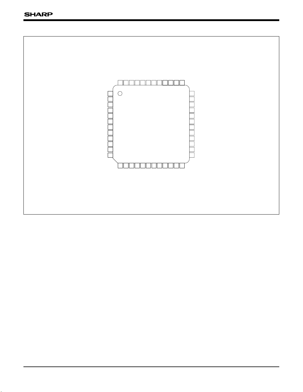
1
48 47 4645 44 4342 41 4039 37
13 14 1516 17 1819 20 2122 23 24
2
3
4
5
6
7
8
9
10
11
12
36
35
34
33
32
31
30
29
28
27
26
25
CCD IN
CLAMP BIAS
IRIS GAMMA
WINDOW
IRIS OUT
V
CC1
GND1
EE NR
SET NR
IRIS IN
SET UP
EE UP
AGC OUT
LPF ADJ
AMP
1 IN
C
1
AGC DET
GND
2
GAMMA ADJ
KNEE ADJ
GAMMA OUT
DL ADJ
HAPA IN
APA CTRL
SYNC
BLK CLP
BCLIP
V
CC2
VIDEO OUT
PEDESTAL
WCLIP
CLAMP
2
AMP2 OUT
GAIN CTRL
C3C2
PGND
FCDSFSPVCCCDS OUT
CLAMP1AGC OP IN
MAX GAIN
AGC OP OUT
AGC CTRL
VCVREF
38
48-PIN QFP
TOP VIEW
(QFP048-P-1010)
(QFP048-P-0707)
PIN CONNECTIONS
Page 3

IR3Y30M/M1
3
PGND
FS
5 V
CDS OUT AGC OP IN
AGC CTRL
VC
VREF LPF ADJ
AGC OUT AMP1 IN
AGC OP
OUT
CLAMP
1
PVcc
FCDS
CLAMP
WINDOW IRIS GAMMA
CLAMP H CLIP
AGC
OP AMP
S/H
FCDS FS
MAX GAIN
C1
GND2
AGC DET
CLP
BLK
GAMMA ADJ
KNEE ADJ
GAMMA OUT
DL ADJ
HAPA IN
APA CTRL
C
2
BCLIP
CLAMP
2
WCLIPPEDESTALBLK CLP
BLK
CLP
GND1Vcc1
EE UP
SET UP
IRIS IN
IRIS OUT BLK
SET NR
EE NR
WINDOW
WINDOW
IRIS GAMMA
CLAMP BIAS
CCD IN
CCD
Vcc
2
VIDEO OUT
SYNC
AMP2
OUT
GAIN
CTRL C3
VREF
LPF
AMP1
GAMMA
KNEE
CLEANING
CLAMP
+
–
AGC
DL
BASE
CLIP
+
+
+
+
+
–
+
–
+
–
+
–
AMP2
CLP
APA AMP
MIXCLAMP
W CLIP
SYNC
OUT
PULSE SEPA
PEDESTAL
SYNC
CLPBUFF
IRIS COMP
IRIS AMP
IRIS OP AMP
CLP
CLP
+
–
+
–
+
–
+
–
+
–
+–
39 38 37 35 36 34
33
31
32
30
29
28
27
26
25
414042434445464748
1
2
3
4
5
8
9
10
11
12
6 7 14 16 17 13 18 19 20 21 22 23 15 24
CLP
5 V5 V
BLK CLP
BLOCK DIAGRAM
Page 4
IR3Y30M/M1
4
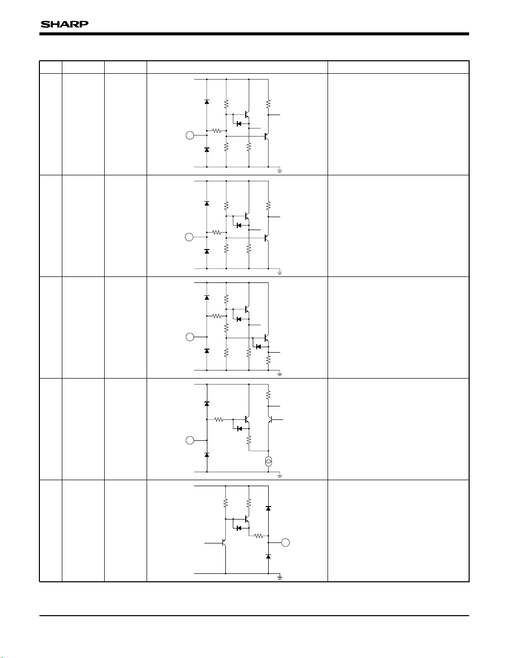
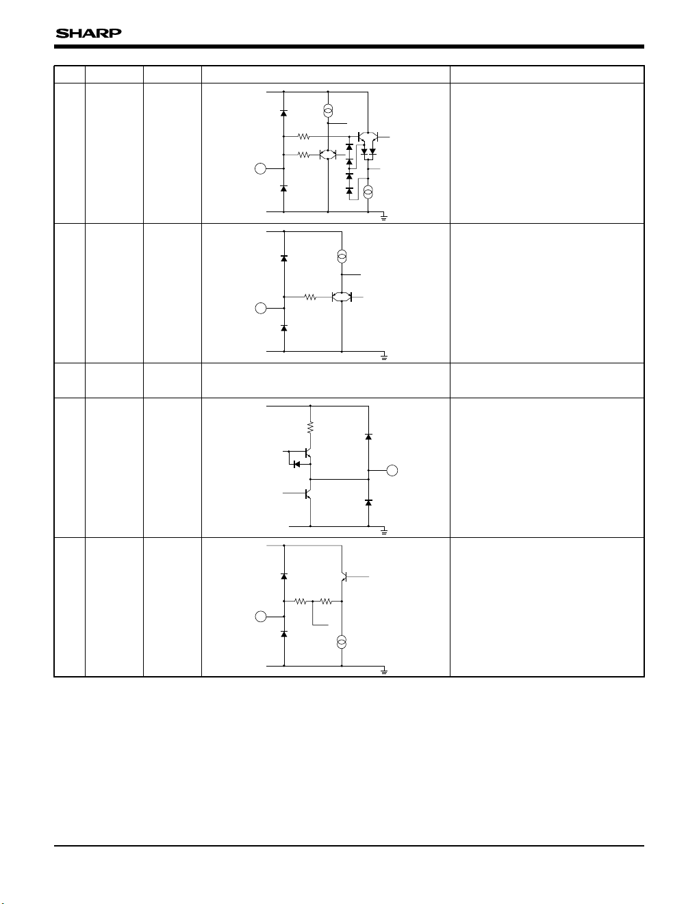
PIN DESCRIPTION
1 CCDIN
2.5 V
Input for the signal from CCD area
sensor. 2.5 V bias applied internally.
PIN NO.
PIN NAME VOLTAGE
EQUIVALENT CIRCUIT DESCRIPTION
1
25 k
200
25 k 9 k
9 k
VCC1
GND
21 k
200
29 k 9 k
9 k
VCC1
GND
2
Feed through level of the input
signal is clamped to this pin voltage.
2.9 V bias applied internally.
Connect capacitor between this pin
and GND.
2.9 V
CLAMP
BIAS
2
3
IRIS
GAMMA
3.1 V
Gamma adjustment of the exposure
circuit. This pin is preset to 3.1 V,
and gamma becomes 0.45 at open.
3
25 k
200
33.8 k 25 k
25 k
6.4 k
VCC1
GND
4
1 k
7 k
18.8 k
190 µ
VCC1
GND
Window pulse input for the exposure
circuit. Outputs the signal while "H".
WINDOW4
20 k
50
1 k
5
VCC1
GND
Output for the exposure signal.
Connect a resistor between this pin
and GND.
2.3 V
IRIS OUT5
Page 5
IR3Y30M/M1
5
6VCC1 Power supply for analog circuits.
PIN NO.
PIN NAME VOLTAGE EQUIVALENT CIRCUIT DESCRIPTION
Ground for analog circuits.GND
17
8 EE NR
Comparator output for electronic
exposure control.
50 k
200
8
VCC1
GND
8
Input of the amplifier for electronic
exposure control. This amplifier has
5 times gain.
IRIS IN
Low reference voltage input of the
comparator for electronic exposure
control.
SET UP
200
2 µ
VCC1
GND
High reference voltage input of the
comparator for electronic exposure
control.
SET NR9
12 EE UP
Output of the comparator for
electronic exposure control.
200
50 k
12
VCC1
GND
13
5 k
40 µ
VCC1
GND
Synchronous signal input.
SYNC13
10
11
Page 6
IR3Y30M/M1
6
14
BLK CLP
Composite pulse input.
(pulse for optical black clamp and
pulse for blanking)
PIN NO.
PIN NAME VOLTAGE
EQUIVALENT CIRCUIT DESCRIPTION
14
5 k
40 µ
40 µ
5 k
VCC1
GND
15
5 k
40 µ
VCC1
GND
Adjustment for the base clip level in
the aperture circuit.
Eliminates the low-level noise of
aperture signal.
When opened, base clip is canceled.
BCLIP
15
16
V
CC2
Power supply for output amplifier
circuits.
100
17
VCC2
GND
Video signal output.
At 75 $ terminated : 1 Vp-p
(Synchronous level 0.3 Vp-p)
1.5 V
VIDEO OUT
17
18
45 k
100 µ
5 k
VCC2
GND
Blanking level adjustment.
100 mV when opened.
2.5 V
PEDESTAL
18
Page 7
IR3Y30M/M1
7
19
WCLIP 3.3 V
White clip adjustment.
120% when opened.
PIN NO.
PIN NAME VOLTAGE
EQUIVALENT CIRCUIT DESCRIPTION
19
35 k
100 µ50 µ
15 k
VCC2
GND
20
50 µ
5 k
5 k
VCC2
GND
Input for encoder circuit. Black level
of input signal is clamped to 2.3 V.
2.3 VCLAMP
2
20
21
AMP2OUT
1.0 V
Output for the gain control amplifier.
21
1 m
100
50 µ
100
VCC1
GND
22
200 µ200 µ
10 k
1.8 k
39 k
VCC1
GND
Controls the output amplitude at pin
No. 21.
Gain is controlled in the range from
6 to 12 dB.
It is approximately 10 dB when this
pin is open.
2.5 V
GAIN
CTRL
22
23
50 µ
50 µ
3 p
3 p
5 k
VCC1
GND
Feedback clamp detector. Connect
capacitor between this pin and GND.
1.8 VC
3
23
Page 8

IR3Y30M/M1
8
24
C
2 1.8 V
Feedback clamp detector. Connect
capacitor between this pin and GND.
When the external DL circuit is used,
this will be input pin to make the
aperture signal.
PIN NO.
PIN NAME VOLTAGE
EQUIVALENT CIRCUIT DESCRIPTION
24
50 µ
50 µ
200
3 p
3 p
50
5 k
µ
VCC1
GND
25
100 µ
40 µ
30.5 k 19.5 k
VCC1
GND
Adjustment for the horizontal
aperture amount. It is approximately
12 dB when this pin is open.
1.8 V
APA CTRL
25
26
HAPA IN
Input for signal from pin 28. This
signal is used as a main signal
when aperture signals are mixed.
26
200
200 µ 100 µ
VCC1
GND
27
200
10 k
4 k
GND
V
CC1
Adjustment for built-in delay line.
When 200 k$ resistor is connected
between this pin and GND, delay
line can be turned off.
1.2 VDL ADJ
27
220 µ
GND
28
VCC1
Gamma and knee processed signal
output.
2.3 V
GAMMA
OUT
28
Page 9

IR3Y30M/M1
9
29
KNEE ADJ
2.8 V
Knee adjustment.
120% when opened.
PIN NO.
PIN NAME VOLTAGE
EQUIVALENT CIRCUIT DESCRIPTION
40 k 10 k
1 k
VCC1
GND
100 µ
29
30
40 k 10 k
10 k
VCC1
GND
100 µ200 µ
Gamma correction adjustment.
0.7 when opened.
2.0 V
GAMMA
ADJ
30
31
GND
2
Ground for analog circuits.
1 k
100 µ
VCC1
GND
32
50 µ
Signal output for AGC control.
Connect resistor between this pin
and GND.
2.0 VAGC DET
32
33
VCC1
GND
50 µ
25 µ
1 p
1 p
10 k
Feedback clamp detector. Connect
capacitor between this pin and GND.
2.0 VC
1
33
34
AMP
1 IN
Input for gamma and knee signal
process.
34
1.65 k
200
170 µ
VCC1
GND
10 k
250 µ
Page 10

IR3Y30M/M1
10
35
LPF ADJ
Adjustment for built-in LPF
characteristic. When connected
resistor is 220 k$ or more between
this pin and GND, LPF can be
turned off.
PIN NO.
PIN NAME VOLTAGE
EQUIVALENT CIRCUIT DESCRIPTION
35
VCC1
GND
3 k
1 k
5 p
200
100
100
VCC1
GND
36
400 µ
AGC signal output.
2.3 VAGC OUT
36
37
V
REF 2.0 V
Reference voltage.
200
VCC1
GND
37
38
200
22 k
8 k
20 k
VCC1
GND
Bias for reference voltage. Connect
capacitor between this pin and GND.
2.0 VV
C
38
39
5 k
50 µ
VCC1
GND
Gain control for AGC amplifier. Be
sure to input the voltage within the
range from 2 to 4 V.
AGC CTRL
39
Page 11

IR3Y30M/M1
11
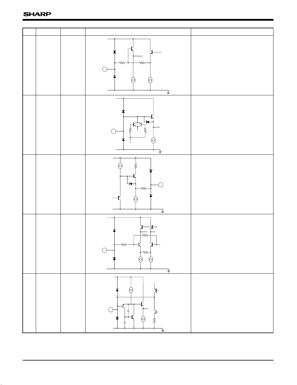
40
AGC OP
OUT
Output of the operation at amplifier
for AGC control.
PIN NO.
PIN NAME VOLTAGE
EQUIVALENT CIRCUIT DESCRIPTION
200
VCC1
GND
40
41
28 k
22 k
50 µ
VCC1
GND
200 µ
Adjustment for AGC amplifier
maximum gain. Maximum gain is 18
dB when opened. When applied
voltage is 0.62 V or less, AGC
circuit turns off and the amplifier is
fixed to 0 dB.
3.3 V
MAX
GAIN
41
42
AGC OP
IN
The operational amplifier for AGC
control.
200
2 µ
VCC1
GND
42
VCC1
GND
43
50 µ
1 k
1 k
Input of AGC amplifier. Black level
is clamped at 2.0 V.
2.0 VCLAMP
1
43
100
750 µ
100
VCC1
GND
44
CDS signal output.
2.4 VCDS OUT
44
Page 12

IR3Y30M/M1
12
45
PV
CC
Power supply for pulse circuits.
PIN NO.
PIN NAME VOLTAGE
EQUIVALENT CIRCUIT DESCRIPTION
46
200
100 µ
PVCC
PGND
Pulse input for sample-hold.
FS
46
47
FCDS
Pulse input for feed-through level
clamp.
47
200
200 µ
PVCC
PGND
Ground for pulse circuits.
PGND
48
Page 13

FUNCTIONAL OPERATION
CDS Circuit
The feed-through level of the input signal is
clamped by the clamp circuit. Then the signal
period is sampled and other periods are held by the
sample and hold circuit, so that signals can be
obtained.
Highlight Clip Circuit
Before the AGC circuit, excessive signals of more
than approximately 0.5 Vp-p are clipped.
AGC Amplifier Circuit
The amplitude of output signals from the AGC
amplifier is externally detected and the gain is
controlled with control signals from the AGC
operational amplifier. Decreasing voltage at pin 41
to 0.62 V or less causes the amplifier to be fixed to
0 dB.
LPF Circuit
The characteristics can be controlled with an
external resistor at pin 35. Increasing the resistor to
220 k$ or more allows signals passing over the
LPF to be output.
Gamma and Knee Corrections Circuits
In order to comply with the characteristics of CRT,
the high-bright part is suppressed. Pin 29 and 30
can be used to control this suppression. If voltage
at pin 30 is increased to 4 V or more gamma will
be 1.
Exposure Circuit
Signals which have not been processed by AGC
are amplified, suppressed by gamma correction,
and then output. Control signals can be generated
by inputting the above signals to pin 10 after
detecting them.
Aperture Circuit
The video articulation can be increased by
enhancing the signal contour. If the built-in delay
line is not used, it can be turned off by using an
external resistor of minimum 200 k$ at pin 27.
To control the aperture amount, use a base clip.
Output Circuit
A load of 75 $ can be driven directly. In addition,
the pedestal level can be controlled vertically.
CAUTIONS
• To control the aperture amount, apply base clip by
controlling pin 15.
• Avoid connecting or disconnecting an external resistor at
pin 27 to prevent the malfunction of the built-in delay line.
• Use the shortest possible distance to connect the bypass
capacitors between the power supply and GND pins. The
addition or removal of any external component should be
determined by how the existing components are mounted.
• This device is electronically sensitive. Handle only at
electrostatically safe work stations.
Gamma Output
Aperture Signal
AMP
2 Output
CCD Signal
FCDS
FS
CDS OUT
IR3Y30M/M1
13
Page 14

IR3Y30M/M1
14
ABSOLUTE MAXIMUM RATINGS (Unless otherwise specified, TA = +25 ˚C)
RECOMMENDED OPERATING CONDITIONS
PARAMETER SYMBOL CONDITIONS UNIT
Supply voltage
V
CC1
, V
CC2
V7
RATING
PVCC 7V
V–0.2 to PV
CC + 0.2Pins 46 (FS) and 47 (FCDS)VIP
VCC V
Except for pins 46 (FS) and 47 (FCDS)
VIA
Input voltage
Comparator output voltage V
SD VVCC
725 mWTA ≤ +25 ˚CPDPower consumption
5.8 mW/˚CT
A > +25 ˚CPD derating ratio
–30 to +75 ˚CT
OPROperating temperature
–55 to +150 ˚CTSTGStorage temperature
PARAMETER SYMBOL APPLICABLE PINS UNIT
Supply voltage V
CC
Pins 6 (VCC1), 16 (VCC2) and 45 (PVCC)
V4.75 to 5.25
RATING
H-aperture signal VH-AP Pin 26 (HAPA IN) mVp-p600 (MAX.)
200 (TYP.) mVp-pPin 1 (CCD IN)V
CCDStandard CCD input signal
15 (MIN.) nsPin 46 (FS)tFSClamp pulse width
15 (MIN.) nsPin 47 (FCDS)t
FCDSSample-hold pulse width
560
4.5
–30 to +70
IR3Y30M IR3Y30M1
Page 15

IR3Y30M/M1
15
ELECTRICAL CHARACTERISTICS
(Unless otherwise specified, TA= +25 ˚C, VCC= 5.0 V, SW conditions/(a), V26= 2.3 V, V34= 2.0 V, V39= 3 V,
R27 = 30 k$, R35 = 22 k$)
PARAMETER SYMBOL CONDITIONS TYP.
Supply current
I
CC1 Measure pin 6 (VCC1). 43.0
MIN.
mA
UNIT
54.5
MAX.
5.4 mA4.3Measure pin 45 (PV
CC).ICC3
7.8 mA5.7Measure pin 16 (VCC2).ICC2
Low frequency
attenuation
G
LF
With signal 1 applied to SG1, measure the
signal attenuation on TP44. FS = 5 V, FCDS
= Signal 2 (FCDS), V
A = TP44 amplitude (f =
100 kHz), VB = TP44 amplitude (f = 10 MHz)
G
LF = 20*LOG (VA/VB)
–30 dB–25
Gain G
CDS
Signal 2 applied to SG1, FS and FCDS,
measure the amplitude on TP44.
SG1 = 200 mVp-p, f = 10 MHz
0–2 dB2
CDS Circuit
3.1 V2.7 2.9V
CP/BIASClamp bias
Low level A
OPL
Measure the voltage on
TP40B. SW40, SW42/(b)
1.0V1.2
AGC Operational Amplifier Circuit
3.9 4.1A
OPHHigh level
V
42 = 3 V,
I
40 = +200 µA
V
42 = 1 V,
I40 = –200 µA
Exposure Operational Amplifier & Comparator Circuits
0.2
V
0
Change the voltage of V
9 and V11, and
measure the voltage on TP8 and TP12.
V
10 = 2.3 V
SW9, SW10, SW11/(b)
I
OPLComparator low level
High level I
OPH 4.70 4.95
AGC Circuit
0.6 Vp-p0.4 0.5
Change the amplitude of signal 3 which is
applied to SG43, and measure the amplitude
on TP36 when TP36's output signal is clipped.
SW43, SW41/(b), Pulse/CLP, V
41 = 0 V,
R35 = 220 k$
H
CLHighlight clip level
0.51 V0.40 0.46
With V
10 = 2.3 V, measure the voltage of V9a
(TP8 : L/H) and V11a (TP12 : H/L).
With V
10 = 2.4 V, measure the voltage of V9b
(TP8 : L/H) and V11b (TP12 : H/L).
G
OP = (V9b-V9a) or (V11b-V11a)
SW9, SW10, SW11/(b)
G
OP
Operational amplifier
gain
Page 16

IR3Y30M/M1
16
PARAMETER SYMBOL CONDITIONS TYP.MIN. UNITMAX.
AGC maximum gain
(1)
G
AMAX1
Apply signal 3 to SG43 and
measure the amplitude on
TP36.
GA1 to GA4 = 20*LOG
(TP36 amplitude/SG43
amplitude)
SW41, SW43/(b),
Pulse/CLP, R35 = 220 k$
2927
dB
31
AGC maximum gain
(2)
AGC minimum gain
AGCOFF gain
G
AMAX2
GAMIN
GAOFF
15.5
–6.5
–2
18.0
–3.5
0
20.5
–0.5
2
SG43 = 20 mVp-p
V39= 4 V, V41= 5 V
SG43 = 20 mVp-p
V39= 4 V, SW41/(a)
SG43 = 400 mVp-p
V39= 2 V, V41= 5 V
SG43 = 200 mVp-p
V39= 4 V, V41= 0 V
Frequency
characteristic (1)
f
A1
Apply signal 4 to SG43.
Increase the frequency of
signal 4 until the frequency
components of the signal on
TP36 are 3 dB lower than
that at f = 100 kHz, and
measure the frequency of
signal 4. SW41/(b),
Pulse/CLP, V
41 = 5 V
When measuring case (2),
adjust the V
39 such that the
amplitude of the output on
TP36 is 200 mVp-p.
4.53.5
MHz
SG43 = 10 mVp-p
R35 = 22 k$
V39 = 4 V
Vp-p0.55 0.75
Apply signal 3 to SG43 and measure the
amplitude on TP36.
SG43 = 50 mVp-p, SW41, SW43/(b),
Pulse/CLP, V
39 = 4 V, V41 = 5 V,
R35 = 220 k$
DA
Output dynamic
range
dB–25
10.0
–35
7.0
SG43 = 200 mVp-p
R35 = 220 k$
SG43 = 10 mVp-p
R35 = 22 k$
V
39 = 4 V
f = 9.5 MHz
Frequency
characteristic (2)
Frequency
characteristic (3)
f
A2
fA3
AGC ON/OFF
switching voltage
V
AGC
Apply signal 3 to SG43, change V41, and
measure the voltage of V
41 when the gain on
TP36 changes from –3.5 to 0 dB. The gain on
TP36 : 20*LOG (TP36 amplitude/SG43 amplitude)
SG43 = 400 mVp-p, SW43, SW41/(b),
Pulse/CLP, V
39 = 2 V, R35 = 220 k$
0.60.4 0.8 V
Reference voltage 1 V
REF Measure the voltage on TP37A. 1.941.84 2.04 V
Reference voltage 2 ∆V
REF2
With I37 = +500 µA, measure the change in
voltage on TP37B.
SW37/(b)
0.150 0.30 V
Reference voltage 3 ∆V
REF3
With I37 = –500 µA, measure the change in
voltage on TP37B.
SW37/(b)
–0.15–0.30 0 V
AGC circuit (contd.)
Page 17

IR3Y30M/M1
17
PARAMETER SYMBOL CONDITIONS TYP.MIN. UNITMAX.
Exposure AMP gain
Exposure Circuit
AMP
1 Circuits
Gamma & Knee Circuits
G
I
Apply signal 3 to SG43 and
measure the amplitude on
TP5.
SW3, SW4, SW43/(b),
Pulse/CLP, BLK
11.510.5 dB12.5
Gamma output level
Output dynamic
range
‹
PRE
DI
0.25
1.5
0.32
1.9
0.40
SG43 = 200 mVp-p
V3= 5 V, V4= 5 V
SW3/(a)
SG43 = 800 mVp-p
V3= 5 V, V4= 5 V
Vp-p
Vp-p
Gamma gain (1) G
‹1
Apply signal 3 to SG34 and
measure the amplitude on
TP28. SW34/(b), Pulse/CLP,
BLK, Input black level = 2 V
410310 mVp-p510
Gamma gain (2)
Gamma gain (3)
G
‹2
G‹3
–6.4
1.3
SG34 = 100 mVp-p
SG34 = 30 mVp-p
SG34 = 200 mVp-p
dB
Black level BI
Measure the voltage on TP5.
SW4/(b), Pulse/CLP, BLK, V4 = 0 V
2.302.15 V2.45
Frequency
characteristic
f
I
Apply signal 4 to SG43. Increase the
frequency of signal 4 until the frequency
components of the signal on TP5 are 3 dB
lower than that at f = 100 kHz, and measure
the frequency of signal 4.
SG43 = 200 mVp-p, V
4 = 5 V,
SW4, SW43/(b), Pulse/CLP, BLK
1.10.7 MHz
Black level offset 1 B
IOFF1 Measure the voltage on TP5.
SW4/(b), Pulse/CLP, BLK
0–50
mV
50
Black level offset 2 B
IOFF2
V4 = 5 V
V
4 = 0 V –50 0 50
70 mVp-p40
Apply signal 3 to SG43 and measure the
amplitude on TP5. SG43 = 200 mVp-p,
SW4, SW43/(b), Pulse/CLP, BLK, V
4 = 0 V
O
WOFF
Window OFF output
level
1.6 V1.2 1.4
Same as in the window OFF output level
measurement. Increase V
4, and measure V4
when the amplitude of output signal on TP5 is
not changed.
V
W
Window ON switching
voltage
3.0 µA0.5 1.2
With V
4 = 5 V, measure input current on pin 4.
SW4/(b)
I
WWindow input current
15 dB13 14
Apply signal 3 to SG34 and measure the
amplitude on TP32. SW34/(b), Pulse/CLP,
BLK, SG34 = 100 mVp-p, Black level = 2 V
G
AMP1AMP1 gain
Vp-p1.20 1.40
Same as in the AMP
1 gain measurement.
Measure output dynamic range on TP32.
D
AMP1
Output dynamic
range
2.1 V1.9 2.0
Measure the voltage on TP32. Pulse/CLP, BLK
B
AMP1Black level
Page 18

IR3Y30M/M1
18
PARAMETER SYMBOL CONDITIONS TYP.MIN. UNITMAX.
Cleaning offset
(1) C
L1 Measure the amplitude of
TP28 between BLK level and
black level. Pulse/CLP, BLK
0–50
mV
50
(2) C
L2
SW30/(a)
SW30/(b),
V
30 = 5 V
–50 0 50
MHz6.0
Apply signal 4 to SG34. Increase the
frequency of signal 4 until the frequency
components of the signal on TP28 are 3 dB
lower than that at f = 100 kHz, and measure
the frequency of signal 4. SW34/(b),
Pulse/CLP, BLK, SG34 = 100 mVp-p,
Black level = 2 V
f
‹
Frequency
characteristic
mVp-p1 100 1 700
Apply signal 3 to SG34 and measure the
amplitude on TP21. SW15, SW23, SW25,
SW29, SW30, SW34/(b), Pulse/CLP, BLK,
SG34 = 50 mVp-p, Black level = 2 V, V
15 = V25
= V29 = V30 = 5 V, V23 = 1.2 V, V26 = 2.3 V
DL
OUTDelay line output
MHz8.0
Apply signal 4 to SG26. Increase the
frequency of signal 4 until the frequency
components of the signal on TP21 are 3 dB
lower than that at f = 100 kHz, and measure
the frequency of signal 4.
SW15, SW25, SW26A/(b), V
15 = 0 V, V25 = 0 V,
Pulse/CLP, BLK, SG26 = 100 mVp-p,
Black level = 2.3 V
f
AMP2
Frequency
characteristic
mVp-p
840Apply signal 3 to SG26 and
measure the amplitude on
TP21. SW26A/(b),
Pulse/CLP, BLK,
SG26 = 100 mVp-p,
Black level = 2.3 V
G
APMAX
Aperture maximum
gain
Aperture & AMP
2 Circuits
Aperture preset gain
Aperture minimum
gain
Base clip output
G
APPRE
GAPMIN
BCL
SW25/(b),
V25 = 5 V
SW25/(b),
V
25 = 0 V
SW15/(b), V15= 0 V
SW25/(b), V25= 5 V
1 130
940
520
450
840
420
350
740
320
250
mVp-p
370
Apply signal 3 to SG26 and
measure the amplitude on
TP21. Pulse/CLP, BLK,
SW15, SW22, SW25, SW26A/(b),
Input black level = 2.3 V,
V
15 = V25 = 0 V
G
AMP2MAX
GAMP2MIN
AMP2 maximum gain
AMP
2 minimum gain
Output dynamic
range
D
AMP2
SG26 = 100 mVp-p,
V22 = 5 V
SG26 = 100 mVp-p,
V22 = 0 V
SG26 = 800 mVp-p,
V22 = 5 V
440 510
280230
2 550
180
2 000
Gamma OFF gain G
‹OFF
Apply signal 3 to SG34 and measure the
amplitude on TP28. SW29, SW30, SW34/(b),
Pulse/CLP, BLK, SG34 = 100 mVp-p,
Black level = 2 V, V
29 = 5 V, V30 = 5 V
510450 mVp-p580
Gamma & Knee Circuits (contd.)
Page 19

IR3Y30M/M1
19
PARAMETER SYMBOL CONDITIONS TYP.MIN. UNITMAX.
Encoder Circuit
Pulse Circuit
White clip (1) WC1 Apply signal 3 to SG20 and
measure the amplitude on
TP17A.
SW20/(b), Pulse/CLP, BLK
2.01.9
V
SW19/(b), V19= 5 V
White clip (2)
White clip preset
WC2
WCPRE
SW19/(b), V19= 0 V
SW19/(a)
1.75
0.85
1.85
0.95
1.95
Setup (1) S
UP1
Measure the amplitude of
TP17A between BLK level
and black level.
Pulse/CLP, BLK
280230
mV
SW18/(b), V18= 5 V
Setup (2)
Setup preset
SUP2
SUPPRE
SW18/(b), V18= 0 V
SW18/(a)
–150
–310
–100
–260
–50
SYNC level V
SYNC
Measure the amplitude of TP17A between
SYNC level and black level.
Pulse/CLP, BLK, SYNC
580530 mV630
Gain G
OUT
Apply signal 3 to SG20 and measure the
amplitude on TP17A. SW20/(b),
Pulse/CLP, BLK, SG20 = 1 Vp-p
0–1 dB1
Output dynamic
range
D
OUT
Apply signal 3 to SG20 and measure the
amplitude of TP17A between SYNC level and
white level. SW19, SW20/(b), V
19 = 5 V,
Pulse/CLP, BLK, SYNC
2.52.2 Vp-p
Frequency
characteristic
f
OUT
Apply signal 4 to SG20. Increase the
frequency of signal 4 until the frequency
components of the signal on TP17B are 3 dB
lower than that at f = 100 kHz, and measure
the frequency of signal 4. SG20 = 1 Vp-p,
SW17, SW20/(b), Pulse/CLP, BLK, SYNC
10 MHz
Output voltage V
OUT
Apply signal 3 to SG20 and measure the
amplitude of TP17B between SYNC level and
white level. SG20 = 1.3 Vp-p, SW17, SW20/(b),
Pulse/CLP, BLK, SYNC
1.00.9 Vp-p
Apply voltages to FCDS, FS, SYNC, BLK and
CLP and measure the threshold voltage of
each circuit.
V
Clamp threshold
voltage
Sample-hold
threshold voltage
Synchronous signal
threshold voltage
Blanking threshold
voltage
Clamp threshold
voltage
V
FCDS
VFS
VSYNC
VBLK
VCP
1.3
1.5
2.5
1.5
3.5
Page 20

IR3Y30M/M1
20
Measurement Waveforms
T/4
2T
Input level
H level
L level
H level
L level
5 V
0 V
5 V
0 V
5 V
0 V
0 V
Signal 4
T/4
T = 1/f f : sampling rate
T/2
50%
100%
Signal 2
(Input)
(FS)
Signal 1
Sine wave amplitude : 200 mVp-p
Low frequency attenuation : 100 kHz/10 MHz (10 MHz = 0 dB)
CLP
SYNC
Sync Pulse
WINDOW
Signal 3
(FCDS)
BLK
Clamp Pulse
Blanking Pulse
Window pulse
4.7 µs
3 µs
11 µs
Page 21

IR3Y30M/M1
21
Test Circuit
36 35 34 33 32 31 30 29 28 27 26 25
13
14
15
16
17
18
19
20
21
22
23
24
123456789101112
48
47
46
45
44
43
42
41
40
39
38
37
0.01
µF
0.01 µF
0.01 µF
0.01 µF
470
µF
0.01 µ
47 µF
47 µF
47 µF
47 µF
0.01 µF
0.01
µF
0.01 µ
0.01 µF
0.01 µF
SG
1
FCDS
FS
TP44
V
42
V41
V39
TP40B
TP40A
TP37B
TP37A
SG43
100 $
100 $
5 V
+
+
+
~
~
~
~
~
TP36
R35
SG34
TP32
V
34
V30
R27
V29
TP28
SG26
V
26
V25
V23
V22
V19
V18
V11V10V9
V4
100
k$
V
3
V15
10 k$
10 k$
10 k$
56
$
+
+
75 $
TP17B
TP17A
CLP
BLK
SYNC
TP12
TP8
TP5
TP21
SG
20
B
A
47 k$
Switching Polarity
(a) (b)
Page 22

PACKAGES FOR CCD AND CMOS DEVICES
22
10.0
±0.2
0.75
TYP.
0.33
±0.1
10.0
±0.2
13.5
±0.4
(11.5)
36
24
37
48
12
1
0.15
±0.05
13
25
(1.75) (1.75)
0.1
±0.1
0.85
±0.2
1.45
±0.2
(1.75)
(1.75)
13.5
±0.4
Package
base plane
0.15
0.15
M
48 QFP (QFP048-P-1010)
PACKAGES (Unit : mm)
36
25
37
48
121
0.15
±0.05
0.1
±0.1
9.0
±0.3
7.0
±0.2
7.0
±0.2
(1.0)(1.0)
(1.0)
(1.0)
0.5
TYP.
0.2
±0.08
9.0
±0.3
0.65
±0.2
1.45
±0.2
24
13
Package
base plane
8.0
±0.2
0.08
0.1
M
48 QFP (QFP048-P-0707)
 Loading...