

Page 1
查询IR2121供应商
CURRENT LIMITING LOW SIDE DRIVER
Data Sheet No. PD-6.018D
IR2121
Features
n Gate drive supply range from 12 to 18V
n Undervoltage lockout
n Current detection and limiting loop to limit driven
power transistor current
n Error lead indicates fault conditions and programs
shutdown time
n Output in phase with input
Description
The IR2121 is a high speed power MOSFET and
IGBT driver with over-current limiting protection circuitry . Latch imm une CMOS technology enables ruggedized monolithic construction. Logic inputs are
compatible with standard CMOS or LSTTL outputs.
The output driver features a high pulse current b uffer
stage designed for minimum cross-conduction. The
protection circuitry detects over-current in the driven
power transistor and limits the gate drive voltage.
Cycle-by-cycle shutdown is programmed by an external capacitor which directly controls the time interval between detection of the over-current limiting
condition and latched shutdown. The output can be
used to drive an N-channel power MOSFET or IGBT
in the low side configuration.
Product Summary
V
OFFSET
IO+/- 1A / 2A
V
OUT
V
CSth
t
(typ.) 150 & 150 ns
on/off
Package
5V max.
12 - 18V
230 mV
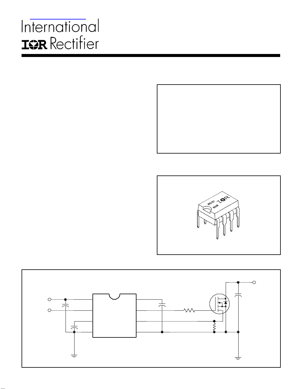
Typical Connection
V
CC
IN
V
CC
IN
ERR
COM
V
CC
OUT
CS
V
TO
LOAD
S
CONTROL INTEGRATED CIRCUIT DESIGNERS MANUAL B-91
Page 2
IR2121
Absolute Maximum Ratings
Absolute Maximum Ratings indicate sustained limits beyond which damage to the device may occur. All voltage parameters are absolute voltages referenced to COM. The Ther mal Resistance and Power Dissipation ratings are measured
under board mounted and still air conditions.
Parameter Value
Symbol Definition Min. Max. Units
V
R
V
V
V
V
ERR
V
P
T
T
T
CC
S
O
IN
CS
D
θJA
J
S
L
Fixed Supply Voltage -0.3 25
Gate Drive Return Voltage VCC - 25 VCC + 0.3
Output Voltage VS - 0.3 V
Logic Input Voltage -0.3 V
Error Signal Voltage -0.3 V
Current Sense Voltage VS - 0.3 V
CC
CC
CC
CC
+ 0.3
+ 0.3
+ 0.3
+ 0.3
V
Package Power Dissipation @ TA ≤ +25°C — 1.0 W
Thermal Resistance, Junction to Ambient — 125 °C/W
Junction Temperature — 150
Storage Temperature -55 150 °C
Lead Temperature (Soldering, 10 seconds) — 300
Recommended Operating Conditions
The Input/Output logic timing diagram is shown in Figure 1. For proper operation the device should be used within the
recommended conditions. The V
Symbol Definition Min. Max. Units
V
CC
V
S
V
O
V
IN
V
ERR
V
CS
T
A
B-92 CONTROL INTEGRATED CIRCUIT DESIGNERS MANUAL
Fixed Supply Voltage VS + 10 VS + 20
Gate Drive Return Voltage -5 5
Output Voltage V
Logic Input Voltage 0 V
Error Signal Voltage 0 V
Current Sense Signal Voltage V
Ambient Temperature -40 125 °C
offset rating is tested with all supplies biased at 15V differential.
S
Parameter Value
S
S
V
CC
CC
CC
V
CC
V
Page 3
IR2121
Dynamic Electrical Characteristics
V
(VCC) = 15V, CL = 3300 pF and TA = 25°C unless otherwise specified. The dynamic electrical characteristics are
BIAS
defined in Figures 2 through 5.
Parameter Value
Symbol Definition Figure Min. Typ. Max. Units Test Conditions
t
on
t
off
t
sd
t
t
t
cs
t
err
Static Electrical Characteristics
V
(VCC) = 15V and TA = 25°C unless otherwise specified. The VIN, VTH and IIN parameters are referenced to COM.
BIAS
The V
O
Symbol Definition Figure Min. Typ. Max. Units Test Conditions
V
V
V
CSTH+
V
CSTH-
V
OH
V
OL
I
QCC
I
IN+
I
IN-
I
CS+
I
CS-
V
CCUV+
V
CCUV-
I
ERR
I
ERR+
I
ERR-
I
O+
I
O-
Turn-On Propagation Delay 7 — 150 200
Turn-Off Propagation Delay 8 — 150 190
ns
ERR Shutdown Propagation Delay 9 — 1.7 2.2 µs
Turn-On Rise Time 10 — 4 3 60
r
Turn-Off Fall Time 11 — 26 35
f
CS Shutdown Propagation Delay 1 2 — 0.7 1.2
CS to ERR Pull-Up Propagation Delay 13 — 9.0 12 C
ns
µs
and IO parameters are referenced to VS .
Parameter Value
Logic “1” Input Voltage 14 2.2 — — VCC = 12V to 18V
IH
Logic “0” Input Voltage 15 — — 0.8 VCC = 12V to 18V
IL
CS Input Positive Going Threshold 16 150 230 320 VCC = 12V to 18V
CS Input Negative Going Threshold 17 130 200 260 VCC = 12V to 18V
High Level Output Voltage, V
Low Level Output V oltage, V
BIAS
O
- V
O
18 — — 100 IO = 0A
19 — — 100 IO = 0A
Quiescent VCC Supply Current 20 — 1.1 2.2 mA
Logic “1” Input Bias Current 21 — 4.5 10
Logic “0” Input Bias Current 22 — — 1.0
“High” CS Bias Current 23 — 4.5 10
“Low” CS Bias Current 24 — — 1.0
VCC Supply Undervoltage Positive Going 25 8.3 8.9 9.6
Threshold
VCC Supply Undervoltage Negative Going 26 7.3 8.0 8.7
Threshold
ERR Timing Charge Current 27 65 100 130
ERR Pull-Up Current 28 8.0 15 —
ERR Pull-Down Current 29 16 30 —
Output High Short Circuit Pulsed Current 3 0 1.0 1.6 —
Output Low Short Circuit Pulsed Current 31 2.0 3.3 —
CONTROL INTEGRATED CIRCUIT DESIGNERS MANUAL B-93
V
mV
V
µA
V
µA
mA
A
ERR
V
=
IN
V
V
V
= 3V or 5V
CS
V
V
= 5V,
IN
ERR < V
V
= 5V,
IN
ERR > V
V
V
= 0V,
O
PW ≤ 10 µs
V
= 15V ,
O
PW ≤ 10 µs
= 270 pF
= 0V or 5V
CS
= 5V
IN
= 0V
IN
= 0V
CS
V
CS
ERR+
V
CS
ERR+
= 0V
IN
V
= 5V
IN
V
IN
= 3V
= 3V
= 0V
Page 4
IR2121
Functional Block Diagram
V
CC
UV
ERR
COM
DETECT
IN
1.8V
ERROR
TIMING
1.8V
PRE
DRIVER
500 ns
BLANK
BUFFER
0.23V
-
+
AMPLIFER
COMPARATOR
Lead Definitions
Lead
Symbol Description
V
CC
IN Logic input for gate driver output (OUT), in phase with OUT
ERR Serves multiple functions; status reporting, linear mode timing and cycle by cycle logic
COM Logic ground
OUT
V
S
CS
Logic and gate drive supply
shutdown
Gate drive output
Gate drive supply return
Current sense input to current sense comparator
V
CC
OUT
V
S
CS
Lead Assignments
8 Lead DIP
IR2121
Part Number
B-94 CONTROL INTEGRATED CIRCUIT DESIGNERS MANUAL
Page 5
Device Information
Process & Design Rule HVDCMOS 4.0 µm
Transistor Count 410
Die Size 104 X 111 X 26 (mil)
Die Outline
Thickness of Gate Oxide 800Å
Connections Material Poly Silicon
First Width 4 µm
Layer Spacing 6 µm
Thickness 5000Å
Material Al - Si (Si: 1.0% ±0.1%)
Second Width 6 µm
Layer Spacing 9 µm
Thickness 20,000Å
Contact Hole Dimension 8 µm X 8 µm
Insulation Layer Material PSG (SiO2)
Thickness 1.5 µm
Passivation Material PSG (SiO2)
(1) Thickness 1.5 µm
Passivation Material Proprietary*
(2) Thickness Proprietary*
Method of Saw Full Cut
Method of Die Bond Ablebond 84 - 1
Wire Bond Method Thermo Sonic
Material Au (1.0 mil / 1.3 mil)
Leadframe Material Cu
Die Area Ag
Lead Plating Pb : Sn (37 : 63)
Pa ckage Types 8 Lead PDIP
Materials EME6300 / MP150 / MP190
Remarks: * Patent Pending
IR2121
CONTROL INTEGRATED CIRCUIT DESIGNERS MANUAL B-95
Page 6
IR2121
IN
CS
OUT
ERR
OUT
IR2121
4
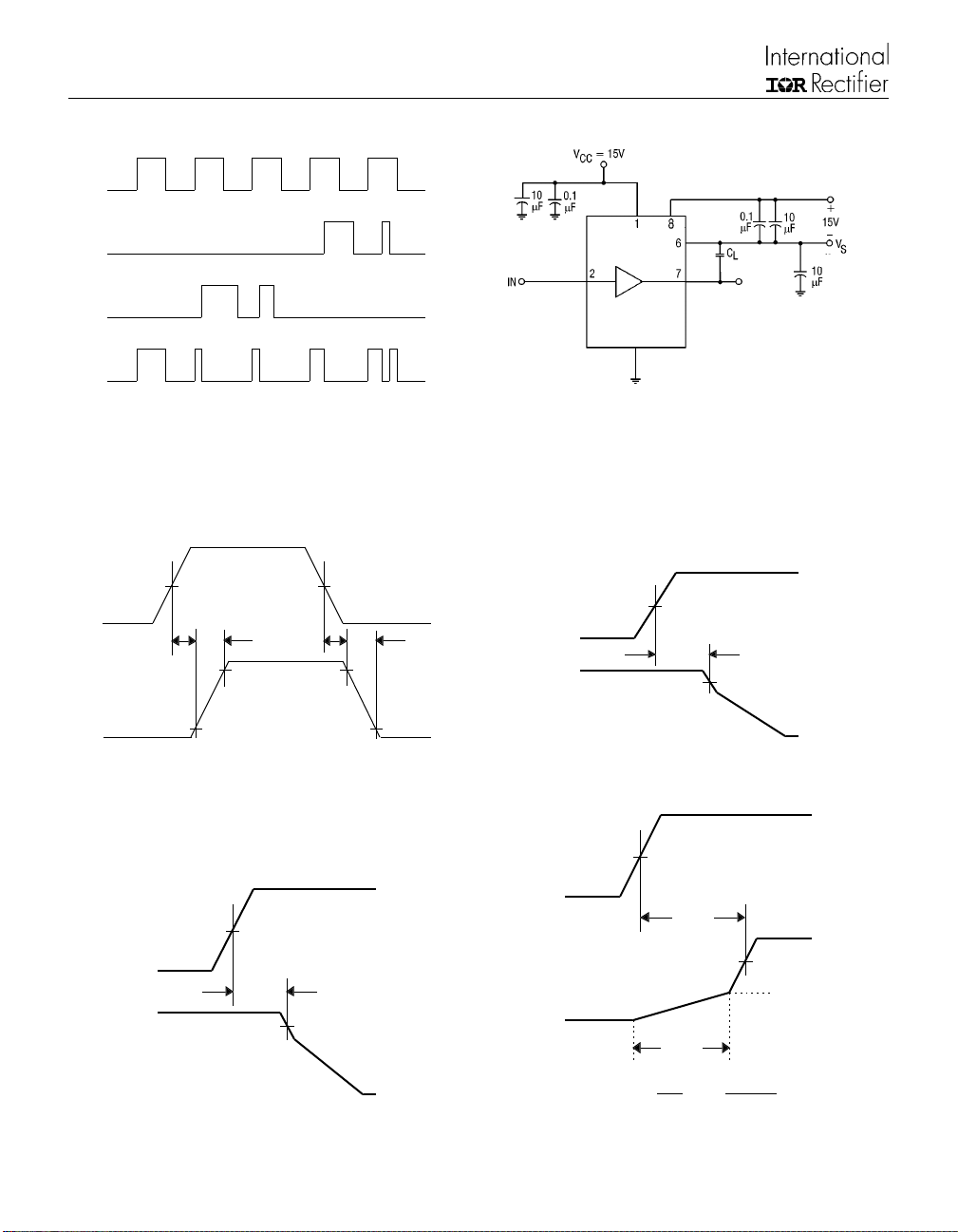
Figure 1. Input/Output Timing Diagram Figure 2. Switching Time T est Circuit
50% 50%
IN
OUT
t
on
t
r
10% 10%
t
off
90% 90%
t
f
CS
OUT
50%
t
cs
90%
V
CC
Figure 3. Switching Time Waveform Definitions Figure 4. ERR Shutdown Waveform Definitions
50%
CS
t
I
dV
ERR
err
50%
1.8V
dt
1.8V
C
100 uA
50%
CS
t
cs
HO
90%
Figure 5. CS Shutdown Waveform Definitions Figure 6. CS to ERR Waveform Definitions
B-96 CONTROL INTEGRATED CIRCUIT DESIGNERS MANUAL
ERR
dt C
=× =×
Page 7

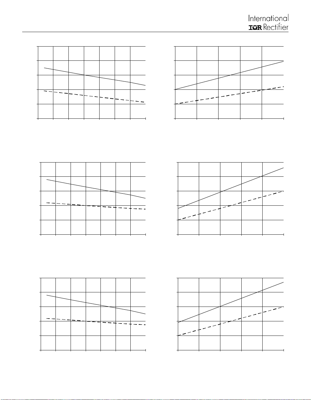
IR2121
s)
T
s)
T
s)
T
s)
T
)
s)
500
400
300
200
Max.
urn-On Delay Time (n
Typ.
100
0
-50 -25 0 25 50 75 100 125
Temperature (°C)
500
400
300
Max.
Typ.
200
urn-On Time (n
100
0
10 12 14 16 18 20
V
Supply Voltage (V)
BIAS
Figure 7A. T urn-On Time vs. Temperature Figure 7B. T urn-On Time vs. V oltage
500
400
300
200
urn-Off Delay Time (n
Max.
Typ.
100
500
400
300
Max.
200
urn-Off Time (ns
Typ.
100
0
-50 -25 0 25 50 75 100 125
Temperature (°C)
0
10 12 14 16 18 20
V
Supply Voltage (V)
BIAS
Figure 8A. T urn-Off Time vs. Temperature Figure 8B. T urn-Off Time vs. Voltage
5.00
4.00
3.00
Max.
2.00
Typ.
1.00
ERR to Output Shutdown Delay Time (µ
0.00
-50 -25 0 25 50 75 100 125
Temperature (°C)
5.00
4.00
3.00
2.00
Max.
Typ.
1.00
ERR to Output Shutdown Delay Time (µ
0.00
10 12 14 16 18 20
V
Supply Voltage (V)
BIAS
Figure 9B. ERR to Output Shutdown vs. VoltageFigure 9A. ERR to Output Shutdown vs. Temperature
CONTROL INTEGRATED CIRCUIT DESIGNERS MANUAL B-97
Page 8

IR2121
C
s)
T
s)
s)
T
)
T
)
C
s)
100
80
60
Max.
Typ.
40
urn-On Rise Time (n
20
0
-50 -25 0 25 50 75 100 125
Temperature (°C)
100
80
Max.
60
Typ.
40
Turn-On Rise Time (n
20
0
10 12 14 16 18 20
V
Supply Voltage (V)
BIAS
Figure 10A. T urn-On Rise Time vs. Temperature Figure 10B. Turn-On Rise Time vs. V oltage
100
80
60
40
urn-Off Fall Time (ns
Max.
Typ.
20
100
80
60
Max.
40
urn-Off Fall Time (ns
Typ.
20
0
-50 -25 0 25 50 75 100 125
Temperature (°C)
Figure 11A. Turn-Off Fall Time vs. Temperature Figure 11B. Turn-Off Fall Time vs. Voltage
2.00
1.60
1.20
Max.
0.80
Typ.
0.40
S to Output Shutdown Delay Time (µ
0.00
-50 -25 0 25 50 75 100 125
Temperature (°C)
Figure 12A. CS to Output Shutdown vs. Temperature Figure 12B. CS to Output Shutdown vs. Voltage
B-98 CONTROL INTEGRATED CIRCUIT DESIGNERS MANUAL
0
10 12 14 16 18 20
V
Supply Voltage (V)
BIAS
2.00
1.60
Max.
1.20
Typ.
0.80
0.40
S to Output Shutdown Delay Time (µ
0.00
10 12 14 16 18 20
V
Supply Voltage (V)
BIAS
Page 9

IR2121
L
)
s)
s)
L
)
L
)
L
)
20.0
16.0
Max.
12.0
Typ.
8.0
CS to ERR Pull-Up Delay Time (µ
4.0
0.0
-50 -25 0 25 50 75 100 125
5.00
4.00
3.00
Min.
2.00
ogic "1" Input Threshold (V
1.00
Temperature (°C)
20.0
16.0
12.0
Max.
Typ.
8.0
CS to ERR Pull-Up Delay Time (µ
4.0
0.0
10 12 14 16 18 20
V
Supply Voltage (V)
BIAS
Figure 13B. CS to ERR Pull-Up vs. VoltageFigure 13A. CS to ERR Pull-Up vs. Temperature
5.00
4.00
3.00
Min.
2.00
ogic "1" Input Threshold (V
1.00
0.00
-50 -25 0 25 50 75 100 125
Temperature (°C)
0.00
10 12 14 16 18 20
V
Logic Supply Voltage (V)
CC
Figure 14A. Logic “1” Input Threshold vs. Temperature Figure 14B. Logic “1” Input Threshold vs. Voltage
5.00
4.00
3.00
2.00
ogic "0" Input Threshold (V
Max.
1.00
0.00
-50 -25 0 25 50 75 100 125
Temperature (°C)
5.00
4.00
3.00
2.00
ogic "0" Input Threshold (V
1.00
Max.
0.00
10 12 14 16 18 20
V
Logic Supply Voltage (V)
CC
Figure 15A. Logic “0” Input Threshold vs. Temperature Figure 15B. Logic “0” Input Threshold vs. Voltage
CONTROL INTEGRATED CIRCUIT DESIGNERS MANUAL B-99
Page 10

IR2121
H
)
C
)
C
)
C
)
C
)
H
)
500
400
Max.
300
Typ.
200
Min.
100
S Input Positive Going Threshold (mV
0
-50 -25 0 25 50 75 100 125
Temperature (°C)
500
400
Max.
300
Typ.
200
Min.
100
S Input Positive Going Threshold (mV
0
10 12 14 16 18 20
V
Floating Supply Voltage (V)
BS
Figure 16A. CS Input Threshold (+) vs. Temperature Figure 16B. CS Input Threshold (+) vs. Voltage
500
400
300
Max.
Typ.
200
Min.
100
S Input Negative Going Threshold (mV
500
400
300
Max.
Typ.
200
Min.
100
S Input Negative Going Threshold (mV
0
-50 -25 0 25 50 75 100 125
Temperature (°C)
Figure 17A. CS Input Threshold (-) vs. Temperature Figure 17B. CS Input Threshold (-) vs. Voltage
1.00
0.80
0.60
0.40
igh Level Output Voltage (V
0.20
Max.
0.00
-50 -25 0 25 50 75 100 125
Temperature (°C)
Figure 18A. High Level Output vs. Temperature Figure 18B. High Level Output vs. Volta g e
B-100 CONTROL INTEGRATED CIRCUIT DESIGNERS MANUAL
0
10 12 14 16 18 20
V
Floating Supply Voltage (V)
BS
1.00
0.80
0.60
0.40
igh Level Output Voltage (V
0.20
Max.
0.00
10 12 14 16 18 20
V
Floating Supply Voltage (V)
BS
Page 11

IR2121
L
)
L
)
)
)
V
)
V
)
1.00
0.80
0.60
0.40
ow Level Output Voltage (V
0.20
Max.
0.00
-50 -25 0 25 50 75 100 125
Temperature (°C)
1.00
0.80
0.60
0.40
ow Level Output Voltage (V
0.20
Max.
0.00
10 12 14 16 18 20
V
Floating Supply Voltage (V)
BS
Figure 19A. Low Level Output vs. Temperature Figure 19B. Low Level Output vs. Voltage
5.00
4.00
3.00
Max.
2.00
Supply Current (mA
CC
1.00
Typ.
5.00
4.00
3.00
2.00
Max.
Supply Current (mA
CC
Typ.
1.00
0.00
-50 -25 0 25 50 75 100 125
Figure 20A. V
25
20
15
10
Max.
Logic "1" Input Bias Current (µA
5
Typ.
0
-50 -25 0 25 50 75 100 125
Figure 21A. Logic “1” Input Current vs. Temperature Figure 21B. Logic “1” Input Current vs. Voltage
Temperature (°C)
Supply Current vs. Temperature Figure 20B. V
CC
Temperature (°C)
0.00
10 12 14 16 18 20
25
20
15
Max.
10
Logic "1" Input Bias Current (µA
Typ.
5
0
10 12 14 16 18 20
V
Supply Voltage (V)
CC
Supply Current vs. Voltage
CC
V
Logic Supply Voltage (V)
CC
CONTROL INTEGRATED CIRCUIT DESIGNERS MANUAL B-101
Page 12

IR2121
)
)
"
)
"
)
"
)
"
)
5.00
4.00
3.00
2.00
Max.
Logic "0" Input Bias Current (µA
1.00
0.00
-50 -25 0 25 50 75 100 125
Temperature (°C)
5.00
4.00
3.00
2.00
Max.
Logic "0" Input Bias Current (µA
1.00
0.00
10 12 14 16 18 20
V
Logic Supply Voltage (V)
CC
Figure 22A. Logic “0” Input Current vs. Temperature Figure 22B. Logic “0” Input Current vs. Voltage
25.0
20.0
15.0
10.0
Max.
High" CS Bias Current (µA
Typ.
5.0
25.0
20.0
15.0
Max.
10.0
High" CS Bias Current (µA
Typ.
5.0
0.0
-50 -25 0 25 50 75 100 125
Temperature (°C)
Figure 23A. “High” CS Bias Current vs. Temperature Figure 23B. “High” CS Bias Current vs. Voltage
5.00
4.00
3.00
2.00
Low" CS Bias Current (µA
Max.
1.00
0.00
-50 -25 0 25 50 75 100 125
Temperature (°C)
Figure 24A. “Low” CS Bias Current vs. Temperature Figure 24B. “Low” CS Bias Current vs. Voltage
B-102 CONTROL INTEGRATED CIRCUIT DESIGNERS MANUAL
0.0
10 12 14 16 18 20
5.00
4.00
3.00
2.00
Low" CS Bias Current (µA
Max.
1.00
0.00
10 12 14 16 18 20
V
Floating Supply Voltage (V)
BS
V
Floating Supply Voltage (V)
BS
Page 13

IR2121
)
)
)
V
)
V
)
)
11.0
10.0
Max.
Typ.
9.0
Min.
8.0
Undervoltage Lockout + (V
CC
7.0
6.0
-50 -25 0 25 50 75 100 125
Temperature (°C)
Figure 25. V
Undervoltage (+) vs. Temperature Figure 26. VCC Undervoltage (-) vs. Temperature
CC
250
200
150
Max.
Typ.
100
Min.
ERR Timing Charge Current (µA
50
11.0
10.0
9.0
Max.
Typ.
8.0
Undervoltage Lockout - (V
Min.
CC
7.0
6.0
-50 -25 0 25 50 75 100 125
Temperature (°C)
250
200
150
Max.
Typ.
100
Min.
ERR Timing Charge Current (µA
50
0
-50 -25 0 25 50 75 100 125
Temperature (°C)
0
10 12 14 16 18 20
V
Logic Supply Voltage (V)
CC
Figure 27A. ERR Timing Charge Current vs. Temperature Figure 27B. ERR Timing Charge Current vs. Voltage
25.0
20.0
Typ.
15.0
Min.
10.0
ERR Pull-Up Current (µA
5.0
0.0
-50 -25 0 25 50 75 100 125
Temperature (°C)
Figure 28A. ERR Pull-Up Current vs. Temperature Figure 28B. ERR Pull-Up Current vs. Voltage
25.0
20.0
15.0
Typ.
10.0
ERR Pull-Up Current (µA
Min.
5.0
0.0
10 12 14 16 18 20
V
Logic Supply Voltage (V)
CC
CONTROL INTEGRATED CIRCUIT DESIGNERS MANUAL B-103
Page 14
IR2121
O
)
O
)
E
)
E
)
O
)
O
)
50
40
Typ.
30
Min.
20
RR Pull-Down Current (µA
10
0
-50 -25 0 25 50 75 100 125
Temperature (°C)
50
40
30
Typ.
20
RR Pull-Down Current (µA
Max.
10
0
10 12 14 16 18 20
V
Logic Supply Voltage (V)
CC
Figure 29A. ERR Pull-Down Current vs.Temperature Figure 29B. ERR Pull-Down Current vs. Voltage
2.50
2.00
Typ.
1.50
Min.
1.00
utput Source Current (A
0.50
2.50
2.00
1.50
Typ.
1.00
utput Source Current (A
Min.
0.50
0.00
-50 -25 0 25 50 75 100 125
Temperature (°C)
Figure 30A. Output Source Current vs.Temperature Figure 30B. Output Source Current vs. Voltage
5.00
4.00
Typ.
3.00
Min.
2.00
utput Sink Current (A
1.00
0.00
-50 -25 0 25 50 75 100 125
Figure 31A. Output Sink Current vs.Temperature Figure 31B. Output Sink Current vs. Voltage
Temperature (°C)
B-104 CONTROL INTEGRATED CIRCUIT DESIGNERS MANUAL
0.00
10 12 14 16 18 20
V
Floating Supply Voltage (V)
BS
5.00
4.00
3.00
Typ.
2.00
utput Sink Current (A
Min.
1.00
0.00
10 12 14 16 18 20
V
Floating Supply Voltage (V)
BS
Page 15

IR2121
T
s)
T
)
)
500
400
300
200
urn-On Time (n
Typ.
100
0
5 7.5 10 12.5 15
Input Voltage (V)
VCC = 15V
500
400
300
200
urn-Off Time (ns
Typ.
100
0
5 7.5 10 12.5 15
Input Voltage (V)
Figure 32A. Turn-On Time vs. Input Temperature Figure 32B. Turn-Off Time vs. Input Voltage
0.00
-3.00
Typ.
Typ.
-6.00
-9.00
Offset Supply Voltage (V
S
V
-12.00
VCC = 15V
-15.00
10 12 14 16 18 20
Figure 33. Maximum V
V
Floating Supply Voltage (V)
BS
Negative Offset vs. Supply
S
Voltage
CONTROL INTEGRATED CIRCUIT DESIGNERS MANUAL B-105
 Loading...