

Page 1
Data Sheet No. PD60139J
IR2105
HALF BRIDGE DRIVER
Features
• Floating channel designed for bootstrap operation
Fully operational to +600V
Tolerant to negative transient voltage
dV/dt immune
• Gate drive supply range from 10 to 20V
• Undervoltage lockout
• 5V Schmitt-triggered input logic
• Cross-conduction prevention logic
• Internally set deadtime
• High side output in phase with input
• Match propagation delay for both channels
Description
The IR2105 is a high voltage, high speed power
MOSFET and IGBT driver with dependent high and
low side referenced output channels. Proprietary
HVIC and latch immune CMOS technologies enable ruggedized monolithic construction. The logic
input is compatible with standard CMOS or LSTTL
outputs. The output drivers feature a high pulse
current buffer stage designed for minimum driver
cross-conduction. The floating channel can be used
to drive an N-channel power MOSFET or IGBT in
the high side configuration which operates from 10
to 600 volts.
Product Summary
V
OFFSET
IO+/- 130 mA / 270 mA
V
OUT
t
(typ.) 680 & 150 ns
on/off
Deadtime (typ.) 520 ns
600V max.
10 - 20V
Packages
8 Lead PDIP
8 Lead SOIC
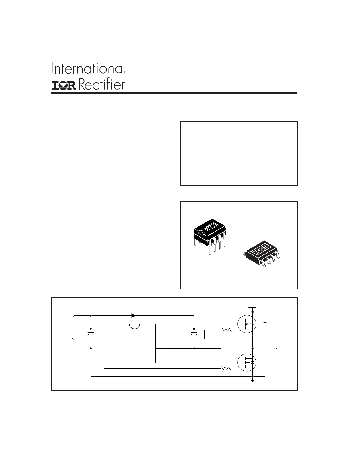
T ypical Connection
V
CC
IN
V
CC
IN
COM
LO
V
HO
V
up to 600V
B
TO
S
LOAD
Page 2
IR2105
Absolute Maximum Ratings
Absolute maximum ratings indicate sustained limits beyond which damage to the device may occur. All voltage parameters are absolute voltages referenced to COM. The thermal resistance and power dissipation ratings are measured
under board mounted and still air conditions.
Symbol Definition Min. Max. Units
V
B
V
S
V
HO
V
CC
V
LO
V
IN
dVs/dt Allowable offset supply voltage transient — 50 V/ns
P
D
Rth
JA
T
J
T
S
T
L
High side floating absolute voltage -0.3 625
High side floating supply offset voltage VB - 25 VB + 0.3
High side floating output voltage VS - 0.3 V
Low side and logic fixed supply voltage -0.3 25
Low side output voltage -0.3 VCC + 0.3
Logic input voltage -0.3 V
Package power dissipation @ TA ≤ +25°C (8 Lead DIP) — 1.0
(8 Lead SOIC) — 0.625
Thermal resistance, junction to ambient (8 Lead DIP) — 125
(8 Lead SOIC) — 200
Junction temperature — 150
Storage temperature -55 150 °C
Lead temperature (soldering, 10 seconds) — 300
CC
B
+ 0.3
+ 0.3
°C/W
V
W
Recommended Operating Conditions
The input/output logic timing diagram is shown in figure 1. For proper operation the device should be used within the
recommended conditions. The VS offset rating is tested with all supplies biased at 15V differential.
Symbol Definition Min. Max. Units
V
B
V
S
V
HO
V
CC
V
LO
V
IN
T
A
Note 1: Logic operational for VS of -5 to +600V. Logic state held for VS of -5V to -VBS.
2
High side floating supply absolute voltage VS + 10 VS + 20
High side floating supply offset voltage Note 1 600
High side floating output voltage V
Low side and logic fixed supply voltage 10 20
Low side output voltage 0 V
Logic input voltage 0 V
Ambient temperature -40 125
S
V
B
CC
CC
V
°C
www.irf.com
Page 3
IR2105
Dynamic Electrical Characteristics
V
(VCC, VBS) = 15V, CL = 1000 pF and TA = 25°C unless otherwise specified.
BIAS
Symbol Definition Min. Typ. Max. Units Test Conditions
t
on
t
off
t
t
DT Deadtime, LS turn-off to HS turn-on & 4 00 520 650
MT Delay matching, HS & LS turn-on/off — — 60
Static Electrical Characteristics
V
BIAS
COM. The VO and IO parameters are referenced to COM and are applicable to the respective output leads: HO or LO.
Symbol Definition Min. Typ. Max. Units Test Conditions
V
V
V
OH
V
OL
I
LK
I
QBS
I
QCC
I
IN+
I
IN-
V
CCUV+VCC
V
CCUV-
I
O+
I
O-
Turn-on propagation delay — 68 0 820 VS = 0V
Turn-off propagation delay — 15 0 220 VS = 600V
Turn-on rise time — 10 0 170
r
Turn-off fall time — 50 90
f
HS turn-on to LS turn-off
(VCC, VBS) = 15V and TA = 25°C unless otherwise specified. The VIN, VTH and IIN parameters are referenced to
Logic “1” (HO) & Logic “0” (LO) Input Voltage 3 — — VCC = 10V to 20V
IH
Logic “0” (HO) & Logic “1” (LO) Input Voltage — — 0.8 VCC = 10V to 20V
IL
High Level Output Voltage, V
Low Level Output Voltage, V
Offset Supply Leakage Current — — 50 VB = VS = 600V
Quiescent VBS Supply Current — 30 55 V
Quiescent VCC Supply Current — 150 270 VIN = 0V or 5V
Logic “1” Input Bias Current — 3 10 VIN = 5V
Logic “0” Input Bias Current — — 1 VIN = 0V
Supply Undervoltage Positive Going 8 8.9 9.8
Threshold
VCC Supply Undervoltage Negative Going 7.4 8.2 9
Threshold
Output High Short Circuit Pulsed Current 130 210 — VO = 0V
Output Low Short Circuit Pulsed Current 270 360 — VO = 15V
BIAS
O
- V
O
— — 100 IO = 0A
— — 100 IO = 0A
ns
V
mV
µA
V
mA
= 0V or 5V
IN
PW ≤ 10 µs
PW ≤ 10 µs
www.irf.com
3
Page 4
IR2105
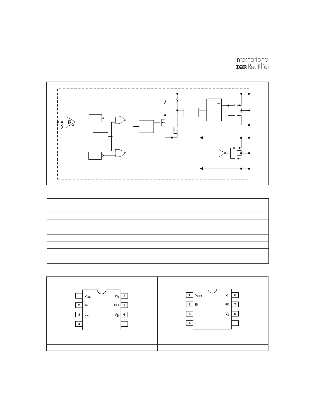
Functional Block Diagram
V
B
HV
LEVEL
DEAD
IN
TIME
DETECT
DEAD
TIME
UV
PULSE
GEN
SHIFT
PULSE
FILTER
Q
R
S
Lead Definitions
Lead
Symbol Description
IN Logic input for high and low side gate driver outputs (HO and LO), in phase with HO
V
B
HO High side gate drive output
V
S
V
CC
LO Low side gate drive output
COM Low side return
High side floating supply
High side floating supply return
Low side and logic fixed supply
HO
V
S
V
LO
COM
CC
Lead Assignments
COM
LO
8 Lead PDIP 8 Lead SOIC
IR2105 IR2105S
4
COM
5
LO
5
www.irf.com
Page 5

IR2105
8 Lead PDIP
8 Lead SOIC
01-3003 01
01-0021 08
www.irf.com
5
Page 6

IR2105
IN
HO
IN
IN
(LO)
(HO)
t
on
50%
t
r
50%
t
off
90% 90%
LO
LO
Figure 1. Input/Output Timing Diagram Figure 2. Switching Time Waveform Definitions
50% 50%
IN
90%
HO
IN
IN
(LO)
(HO)
10% 10%
50% 50%
LO
HO
t
f
HO
LO
Figure 3. Deadtime Waveform Definitions Figure 4. Delay Matching Waveform Definitions
DT
90%
10%
10%
DT
MT
10%
90%
6
MT
HOLO
www.irf.com
Page 7

IR2105
1400
1200
1000
Max.
800
600
Typ.
400
200
Turn-On Delay Time (ns)
0
-50 -25 0 25 50 75 100 125
Temperature (oC)
Figure 6A. Turn-On Time vs Temperature
500
400
300
Max.
200
100
Turn-Off Delay Time (ns)
Typ.
0
-50 -25 0 25 50 75 10 0 125
Temperature (oC)
1400
1200
Max.
1000
800
Typ.
600
400
200
Turn-On Delay Time (ns)
0
10 12 14 16 18 20
VBIAS Supply Voltage (V)
Figure 6B. Turn-On Time vs Voltage
500
400
300
Max.
200
Typ .
100
Turn-Off Delay Time (ns)
0
10 12 14 16 18 20
VBIAS Supply Voltage (V)
Figure 7A. Turn-Off Time vs Temperature
500
400
300
200
Max.
100
Turn-On Rise Time (ns)
Typ.
0
-50 -25 0 25 50 75 100 125
Temperature (oC)
Figure 9A. T urn-On Rise Time
vs Temperature
www.irf.com
Figure 7B. Turn-Off Time vs Voltage
500
400
300
Max .
200
100
Turn-On Rise Time (ns)
Typ.
0
10 12 14 16 18 20
VBIAS Supply Voltage (V)
Figure 9B. T urn-On Rise Time
vs V oltage
7
Page 8

IR2105
200
150
100
Turn-Off Fall Time (ns)
Max.
Typ.
50
0
-50 -25 0 25 50 75 100 125
Temperature (oC)
Figure 10A. Turn Off Fall Time
vs Temperature
1400
1200
1000
800
Max .
600
p.
Ty
400
Deadtime (ns)
Min.
200
0
-50 -2 5 0 25 50 75 100 125
Temperature (
o
C)
200
150
Max.
100
Typ.
50
Turn-Off Fall Time (ns)
0
10 12 14 16 18 20
VBIAS Supply Voltage (V)
Figure 10B. Turn Off Fall Time vs Voltage
1400
1200
1000
Max .
800
Ty p .
600
Deadtime (ns)
400
Min.
200
0
10 12 14 16 18 20
VBIAS Supply Voltage (V)
Figure 11A. Deadtime vs Temperature
8
7
6
5
4
Min.
3
2
Input Voltage (V)
1
0
Temperature (oC)
-50 -25 0 25 50 75 100 125
Temperature (oC)
Figure12A. Logic "1" (HO) & Logic "0" (LO)
Input Voltage vs Temperature
8
Figure 11B. Deadtime vs Voltage
8
7
6
5
4
Min.
3
2
Input Voltage (V)
1
0
10 12 14 16 18 20
VBIAS Supply Voltage (V)
Figure 12B. Logic "1" (HO) & Logic "0" (LO)
Input Voltage vs Voltage
www.irf.com
Page 9

IR2105
4
3.2
2.4
1.6
Max .
Input Voltage (V)
0.8
0
-50 - 25 0 25 50 75 100 125
Temperature (oC)
Figure 13A. Logic "0"(HO) & Logic "1"(LO)
Input Voltage vs Temperature
1
0.8
0.6
0.4
0.2
Max.
High Level Output Voltage (V)
0
-50 -25 0 25 50 75 100 125
Temperature (oC)
4
3.2
2.4
1.6
Input Voltage (V)
Max.
0.8
0
10 12 14 16 18 20
Vcc Supply Voltage (V)
Figure 13B. Logic "0"(HO) & Logic "1"(LO)
Input Voltage vs Voltage
1
0.8
0.6
0.4
0.2
Max.
High Level Output Voltage (V)
0
10 12 14 16 18 20
Vcc Supply Voltage (V)
Figure 14A. High Level Output vs Temperature
1
0.8
0.6
0.4
0.2
Low Level Output Voltage (V)
Max .
0
-50 -25 0 25 50 75 100 125
Temperature (oC)
Figure 15A. Low Le vel Output
vs Temperature
www.irf.com
Figure 14B. High Level Output vs Voltage
1
0.8
0.6
0.4
0.2
Max .
Low Level Output Voltage (V)
0
10 12 14 16 18 20
Vcc Supply Voltage (V)
Figure 15B. Lo w Level Output vs V oltage
9
Page 10

IR2105
500
400
300
200
100
Max.
0
Offset Supply Leakge Current (µA)
-50-25 0 25 50 75100125
Temperature (oC)
Figure 16A. Offset Supply Current
vs Temperature
150
120
90
60
Max .
30
VBS Supply Current (µA)
0
Ty p .
-50-250 255075100125
Temperature (oC)
500
400
300
200
Max.
100
0
Offset Supply Leakge Current (µA)
0 200 400 600 800
VB Boost Voltage (V)
Figure 16B. Offset Supply Current vs Voltage
150
120
90
60
Max.
30
VBS Supply Current (µA)VCC Supply Current (µA)
Typ.
0
10 12 14 16 18 20
VBS Floating Supply Voltage (V)
Figure 17A. V
BS Supply Current
vs Temperature
700
600
500
400
Max.
300
200
100
VCC Supply Current (µA)
Typ.
0
-50 -25 0 25 50 75 100 125
Temperature (oC)
Figure 18A. Vcc Supply Current
vs Temperature
10
Figure 17B. VBS Supply Current vs Voltage
700
600
500
400
300
Max.
200
100
Typ.
0
10 12 14 16 18 20
Vcc Supply Voltage (V)
Figure 18B. Vcc Supply Current vs Voltage
www.irf.com
Page 11

IR2105
30
25
20
15
Max .
10
Max
5
Logic “1” Input Current (µA)
Ty p .
0
-50 -25 0 25 50 75 100 12 5
Temperature (oC)
Figure 19A. Logic "1" Input Current
vs Temperature
5
4
3
2
Max.
1
Logic “0” Input Current (µA)
0
-50 -25 0 25 50 75 100 125
Temperature (oC)
30
25
20
15
Max .
10
5
Logic “1” Input Current (µA)
Ty p.
0
10 12 14 16 18 20
Vcc Supply Voltage (V)
Figure 19B. Logic "1" Input Current
vs Voltage
5
4
3
2
Max.
1
Logic “0” Input Current (µA)
0
10 12 14 16 18 20
Vcc Supply Voltage (V)
Figure 20A. Logic "0" Input Current vs
Temperature
11
Max .
10
Typ .
9
Min.
8
7
VCC UVLO Threshold +(V)
6
-50 - 25 0 25 50 75 100 125
Temperature (
o
C)
Figure 21A. Vcc Undervoltage Threshold(+)
vs Temperature
www.irf.com
Figure 20B. Logic "0" Input Current vs V oltage
11
10
Max .
9
Typ.
Typ.
8
7
Min.
VCC UVLO Threshold -(V)
6
-50-25 0 25 50 75100125
Temperature (oC)
Figure 21B. Vcc UndervoltageThreshold (-)
vs Temperature
11
Page 12

IR2105
500
400
Typ .
300
200
100
Min.
Output Source Current (mA)
0
-50-25 0 25 50 75100125
Temperature (oC)
Figure 22A. Output Source Current
vs Temperature
700
600
Ty p .
500
400
300
Min.
200
100
Output Sink Current (mA)
0
-50 -25 0 25 50 75 100 125
Temperature (oC)
500
400
300
200
Typ.
100
Output Source Current (mA)
0
10 12 14 16 18 20
Min.
Min.
VBIAS Supply Voltage (V)
Figure 22B. Output Source Current
vs Voltage
700
600
500
400
Typ.
300
200
Min.
100
Output Sink Current (mA)
0
10 12 14 16 18 20
VBIAS Supply Voltage (V)
Figure 23A. Output Sink Current
vs Temperature
Figure 23B. Output Sink Current
vs Voltage
WORLD HEADQUARTERS: 233 Kansas St., El Segundo, California 90245 Tel: (310) 322 3331
IR GREAT BRITAIN: Hurst Green, Oxted, Surrey RH8 9BB, UK Tel: ++ 44 1883 732020
IR JAPAN: K&H Bldg., 2F, 30-4 Nishi-Ikebukuro 3-Chome, Toshima-Ku, Tokyo, Japan 171-0021 Tel: 8133 983 0086
IR HONG KONG: Unit 308, #F, New East Ocean Centre, No. 9 Science Museum Road, Tsimshatsui East, Kowloon, Hong
Kong Tel: (852) 2803-7380
Data and specifications subject to change without notice. 11/29/99
12
www.irf.com
 Loading...