

Page 1
查询IR2104(S)供应商
Data Sheet No. PD60046-P
IR2104
(S)
HALF-BRIDGE DRIVER
Features
Floating channel designed for bootstrap operation
•
Fully operational to +600V
Tolerant to negative transient voltage
dV/dt immune
Gate drive supply range from 10 to 20V
•
Undervoltage lockout
•
3.3V , 5V and 15V input logic compatib le
•
Cross-conduction prevention logic
•
Internally set deadtime
•
High side output in phase with input
•
Shut down input turns off both channels
•
Matched propagation delay for both channels
•
Description
The IR2104(s) are high voltage, high speed power
MOSFET and IGBT drivers with dependent high and
low side referenced output channels. Proprietary HVIC
and latch immune CMOS technologies enable ruggedized monolithic construction. The logic input is compatible with standard CMOS or LSTTL output, down to
3.3V logic. The output driv ers feature a high pulse current buffer stage designed f or minimum driver cross-conduction. The floating channel can be used to drive an Nchannel power MOSFET or IGBT in the high side configuration which operates from 10 to 600 volts.
Product Summary
V
OFFSET
+/ - 130 mA / 270 mA
I
O
V
OUT
t
(typ.) 680 & 150 ns
on/off
Deadtime (typ.) 520 ns
600V max.
10 - 20V
Packages
8 Lead SOIC
IR2104S
8 Lead PDIP
IR2104
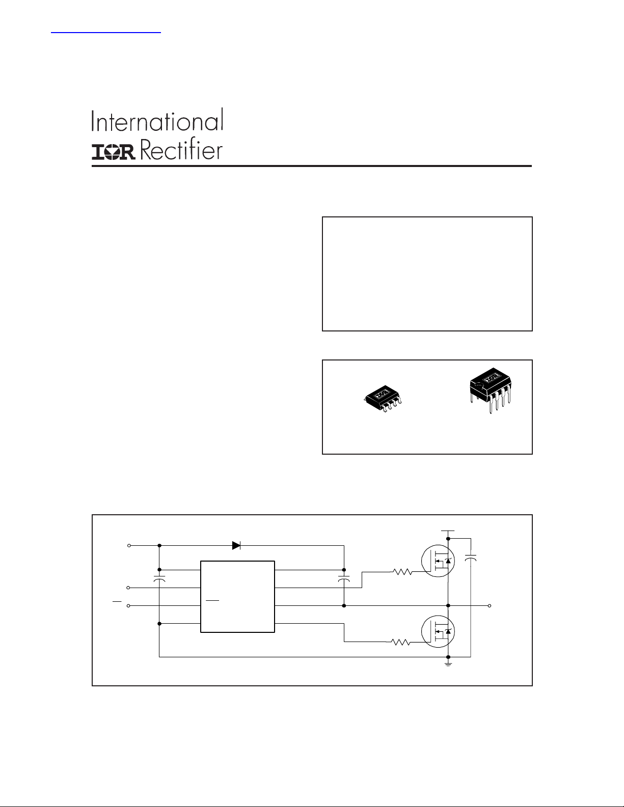
T ypical Connection
up to 600V
V
CC
V
CC
IN
SD
(Refer to Lead Assignment for correct pin configuration) This/These diagram(s) show electrical
connections only. Please refer to our Application Notes and DesignTips for proper circuit board layout.
IN
SD
www.irf.com 1
V
HO
V
LOCOM
B
TO
S
LOAD
Page 2
IR2104
(S)
Absolute Maximum Ratings
Absolute maximum ratings indicate sustained limits beyond which damage to the device may occur. All voltage
parameters are absolute voltages referenced to COM. The thermal resistance and power dissipation ratings are
measured under board mounted and still air conditions.
Symbol Definition Min. Max. Units
V
B
V
S
V
HO
V
CC
V
LO
V
IN
dVs/dt Allowable offset supply voltage transient — 50 V/ns
P
D
Rth
JA
T
J
T
S
T
L
High side floating absolute voltage -0.3 625
High side floating supply offset voltage VB - 25 VB + 0.3
High side floating output voltage VS - 0.3 V
Low side and logic fixed supply voltage -0.3 25
Low side output voltage -0.3 VCC + 0.3
Logic input voltage (IN & SD) -0.3 V
Package power dissipation @ TA ≤ +25°C (8 lead PDIP) — 1.0
(8 lead SOIC) — 0.625
Thermal resistance, junction to ambient (8 lead PDIP) — 125
(8 lead SOIC) — 200
Junction temperature — 150
Storage temperature - 55 150
Lead temperature (soldering, 10 seconds) — 300
CC
B
+ 0.3
+ 0.3
V
W
°C/W
°C
Recommended Operating Conditions
The Input/Output logic timing diagram is shown in Figure 1. For proper operation the device should be used within the
recommended conditions. The VS offset rating is tested with all supplies biased at 15V differential.
Symbol Definition Min. Max. Units
V
B
V
S
V
HO
V
CC
V
LO
V
IN
T
A
Note 1: Logic operational f or VS of -5 to +600V. Logic state held f or VS of -5V to -VBS. (Please refer to the Design Tip
DT97-3 for more details).
2
High side floating supply absolute voltage VS + 10 VS + 20
High side floating supply offset voltage Note 1 600
High side floating output voltage V
Low side and logic fixed supply voltage 10 20
Low side output voltage 0 V
Logic input voltage (IN & SD)0V
Ambient temperature -40 125
S
V
B
CC
CC
°C
www.irf.com
V
Page 3
IR2104
(S)
Dynamic Electrical Characteristics
V
(VCC, VBS) = 15V, CL = 1000 pF and TA = 25°C unless otherwise specified.
BIAS
Symbol Definition Min. Typ. Max. Units Test Conditions
t
on
t
off
t
sd
t
t
DT Deadtime, LS turn-off to HS turn-on & 400 520 650
MT Delay matching, HS & LS turn-on/off ——60
Turn-on propagation delay — 680 820 VS = 0V
Turn-off propagation delay — 150 220 VS = 600V
Shutdown propagation delay — 160 220
Turn-on rise time — 100 170
r
Turn-off fall time — 50 90
f
HS turn-on to LS turn-off
ns
Static Electrical Characteristics
V
(VCC, VBS) = 15V and TA = 25°C unless otherwise specified. The VIN, VTH and IIN parameters are referenced to
BIAS
COM. The VO and IO parameters are referenced to COM and are applicable to the respective output leads: HO or LO.
Symbol Definition Min. Typ. Max. Units Test Conditions
V
SD,TH+
V
SD,TH-
V
V
I
QBS
I
QCC
I
V
CCUV+
V
CCUV-
I
V
V
I
I
I
IH
OH
OL
LK
IN+
IN-
O+
O-
Logic “1” (HO) & Logic “0” (LO) input voltage 3 —— VCC = 10V to 20V
Logic “0” (HO) & Logic “1” (LO) input voltage ——0.8 VCC = 10V to 20V
IL
SD input positive going threshold 3 —— VCC = 10V to 20V
SD input negative going threshold ——0.8 VCC = 10V to 20V
High level output voltage, V
Low level output voltage, V
Offset supply leakage current ——50 VB = VS = 600V
Quiescent VBS supply current — 30 55 V
Quiescent VCC supply current — 150 270 VIN = 0V or 5V
Logic “1” input bias current — 310 VIN = 5V
Logic “0” input bias current ——1V
VCC supply undervoltage positive going 8 8.9 9.8
threshold
VCC supply undervoltage negative going 7.4 8.2 9
threshold
Output high short circuit pulsed current 130 210 — VO = 0V
Output low short circuit pulsed current 270 360 — VO = 15V
BIAS
O
- V
O
——100 IO = 0A
——100 IO = 0A
V
mV
µA
V
mA
IN
PW ≤ 10 µs
PW ≤ 10 µs
= 0V or 5V
= 0V
IN
www.irf.com
3
Page 4
IR2104
(S)
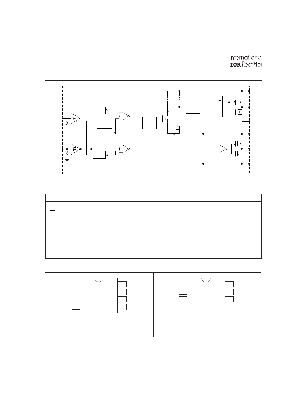
Functional Block Diagram
V
B
HV
DEAD
TIME
IN
UV
DETECT
PULSE
GEN
LEVEL
SHIFT
PULSE
FILTER
Q
R
S
Vcc
SD
DEAD
TIME
Lead Definitions
Symbol Description
IN Logic input for high and low side gate driver outputs (HO and LO), in phase with HO
SD
V
B
HO High side gate drive output
V
S
V
CC
LO Low side gate drive output
COM Low side return
Logic input for shutdown
High side floating supply
High side floating supply return
Low side and logic fixed supply
HO
V
S
V
LO
COM
CC
Lead Assignments
1
V
CC
2
IN
3
SD
4
COM
8 Lead PDIP 8 Lead SOIC
IR2104 IR2104S
4
V
HO
V
LO
V
8
B
7
6
S
5
1
CC
IN
2
SD
3
COM
4
V
HO
V
LO
8
B
7
6
S
5
www.irf.com
Page 5

IR2104
(S)
IN
SD
HO
LO
Figure 1. Input/Output Timing Diagram
SD
50%
t
sd
HO
90%
LO
Figure 3. Shutdown W aveform Definitions
(LO)
IN
50%
t
off
t
f
IN
(HO)
t
on
50%
t
r
90% 90%
LO
HO
Figure 2. Switching Time W aveform Definitions
IN
HO
LO
10% 10%
50% 50%
90%
10%
DT DT
90%
10%
IN
(LO)
50% 50%
IN
(HO)
HO
LO
10%
MT
90%
Figure 5. Delay Matching W aveform Definitions
www.irf.com
Figure 4. Deadtime Waveform Definitions
MT
HOLO
5
Page 6

IR2104
s
(S)
1400
1200
1000
Max.
800
600
Typ.
400
200
Turn-On Delay Time (ns)
0
-50 -25 0 25 50 75 10 0 12 5
T emperature (°C) VBIAS Supply Voltage (V)
1400
1200
Max .
1000
800
Typ.
600
400
200
Turn-On Delay Time (ns)
0
10 12 14 16 18 20
Figure 6A. Turn-On Time vs T emperature Figure 6B. T urn-On Time vs Supply V oltage
1000
800
600
400
200
Turn-On Delay Time (ns
0
0 2 4 6 8 101214161820
Max.
Typ
.
Input Voltage (V)
Figure 6C. Turn-On T ime vs Input Voltage
500
400
300
Max .
200
100
Ty p .
Turn-Off Delay Time (ns)
0
-50 -25 0 25 50 75 100 12 5
T emperature (°C)
Figure 7A. T urn-Off Time vs T emperature
500
400
Max.
300
200
Typ.
100
Turn-Off Delay Time (ns)
0
10 12 14 16 18 20
VBIAS Supply Voltage (V)
Figure 7B. Turn-Off T ime vs Supply V oltage
6
1000
800
600
400
200
Turn-Off Delay Time (n
0
02468101214161820
Max.
Typ
Input Voltage (V)
Figure 7C. T urn-Off Time vs Input Voltage
www.irf.com
Page 7

IR2104
(S)
500
400
300
Max.
200
100
Ty p .
Shutdown Delay Time (ns)
0
-50 -25 0 25 50 75 100 125
Temperature (°C)
Figure 8A. Shutdown Time vs T emperature
500
400
300
200
Max
.
100
Turn-On Rise Time (ns)
Ty p .
0
-50 -25 0 25 50 75 100 125
Temperature (°C)
500
400
Max.
300
200
Typ.
100
Shutdown Delay Time (ns)
0
10 12 14 16 18 20
VBIAS Supply Voltage (V)
Figure 8B. Shutdown Time vs V oltage
500
400
300
Max .
200
100
Turn-On Rise Time (ns)
Ty p .
0
10 12 14 16 18 20
VBIAS Supply Voltage (V)
Figure 9A. T urn-On Rise Time
vs Temperature
200
150
100
Max
.
50
Ty p .
Turn-Off Fall Time (ns)
0
-50 -25 0 25 50 75 100 125
Temperature (°C)
Figure 10A. T urn-Off Fall Time
vs Temperature
www.irf.com
Figure 9B. Turn-On Rise Time vs Voltage
200
150
Max .
100
50
Ty p .
Turn-Off Fall Time (ns)
0
10 12 14 16 18 20
VBIAS Supply Voltage (V)
Figure 10B. T urn-Off Fall T ime vs Voltage
7
Page 8

IR2104
(S)
1400
1200
1000
800
Max.
600
Ty p.
Deadtime (ns)
400
Min.
200
0
-50 -25 0 25 50 75 100 125
T emperature (°C) VBIAS Supply Voltage (V)
Figure 1 1A. Deadtime vs T emperature
8
7
6
5
4
Min.
3
2
Input Voltage (V)
1
0
-50-25 0 25 50 75100125
Temperature (°C)
1400
1200
1000
Max .
800
600
Deadtime (ns)
Ty p .
400
Min.
200
0
10 12 14 16 18 20
Figure 11B. Deadtime vs V oltage
8
7
6
5
4
Min .
3
2
Input Voltage (V)
1
0
10 12 14 16 18 20
Vcc Supply Voltage (V)
Figure 12A. Logic "1" (HO) & Logic “0” (LO)
& Inactive SD Input Voltage
vs Temperature
4
3.2
2.4
1.6
.
Max
Input Voltage (V)
0.8
0
-50 -25 0 25 50 75 100 125
Temperature (°C)
Figure 13A. Logic "0" (HO) & Logic “1” (LO)
& Active SD Input Voltage
vs Temperature
8
Figure 12B. Logic "1" (HO) & Logic “0” (LO)
& Inactive SD Input V oltage
vs Voltage
4
3.2
2.4
1.6
Max.
Input Voltage (V)
0.8
0
10 12 14 16 18 20
Vcc Supply Voltage (V)
Figure 13B. Logic "0" (HO) & Logic “1” (LO)
& Active SD Input Voltage
vs V oltage
www.irf.com
Page 9

IR2104
(S)
1
0.8
0.6
0.4
Max .
0.2
0
High Level Output Voltage (V)
-50 -25 0 25 50 75 100 125
T emperature (°C)
Figure 14A. High Level Output
vs Temperature
1
0.8
0.6
0.4
0.2
Max .
Low Level Output Voltage (V)
0
-50 -25 0 25 50 75 100 125
Temperature (°C)
1
0.8
0.6
0.4
Max.
0.2
High Level Output Voltage (V)
0
10 12 14 16 18 20
Vcc Supply Voltage (V)
Figure 14B. High Level Output vs Voltage
1
0.8
0.6
0.4
0.2
Max.
Low Level Output Voltage (V)
0
10 12 14 16 18 20
Vcc Supply Voltage (V)
Figure 15A. Low Level Output
vs Temperature
500
400
300
200
100
Max .
0
Offset Supply Leakage Current (µA)
-50-25 0 25 50 75100125
Temperature (°C)
Figure 16A. Offset Supply Current
vs Temperature
www.irf.com
Figure 15B. Low level Output vs V oltage
500
400
300
200
100
Max.
0
Offset Supply Leakage Current (µA)
0 100 200 300 400 500 600
VB Boost Voltage (V)
Figure 16B. Offset Supply Current
vs V oltage
9
Page 10

IR2104
(S)
150
120
90
60
Max .
30
VBS Supply Current (µA)
Ty p .
0
-50 -25 0 25 50 75 100 12 5
T emperature (°C)
Figure 17A. VBS Supply Current
vs Temperature
700
600
500
400
Max .
300
200
Vcc Supply Current (µA)
100
Ty p .
0
-50 -25 0 25 50 75 100 125
Temperature (°C)
150
120
90
60
Max.
30
VBS Supply Current (µA)
Typ.
0
10 12 14 16 18 20
VBS Floating Supply Voltage (V)
Figure 17B. V
BS Supply Current
vs V oltage
700
600
500
400
300
Max .
200
Vcc Supply Current (µA)
100
Ty p .
0
10 12 14 16 18 20
Vcc Supply Voltage (V)
Figure 18A. Vcc Supply Current
vs Temperature
30
25
20
15
10
Max .
5
Logic 1” Input Current (µA)
Ty p .
0
-50-25 0 25 50 75100125
Temperature (°C)
Figure 19A. Logic"1" Input Current
vs Temperature
10
Figure 18B. Vcc Supply Current vs Voltage
30
25
20
15
10
Max .
5
Ty p .
Logic 1” Input Current (µA)
0
10 12 14 16 18 20
Vcc Supply Voltage (V)
Figure 19B. Logic"1" Input Current
vs V oltage
www.irf.com
Page 11

IR2104
(S)
5
4
3
2
Max.
1
Logic “0” Input Current (µA)
0
-50 -25 0 25 50 75 100 125
T emperature (°C)
Figure 20A. Logic "0" Input Current
vs Temperature
11
Max .
10
Typ .
9
Min .
8
7
VCC UVLO Threshold +(V)
6
-50-25 0 25 50 75100125
Temperature (°C)
Figure 21A. Vcc Undervoltage Threshold(+)
vs Temperature
5
4
3
2
Max.
1
Logic "0" Input Current (uA)
0
10 12 14 16 18 20
VCC Supply Voltage (V)
Figure 20B. Logic "0" Input Current
vs Voltage
11
10
Max.
9
Typ.
8
7
Min.
VCC UVLO Threshold - (V)
6
-50 -25 0 25 50 75 100 125
Temperature (°C)
Figure 21B. Vcc Undervoltage Threshold(-)
vs Temperature
500
400
Typ.
300
200
100
Min.
Output Source Current (mA)
0
-50 -25 0 25 50 75 100 125
Temperature (°C)
Figure 22A. Output Source Current
vs Temperature
www.irf.com
500
400
300
200
Typ.
100
Output Source Current (mA)
Min.
0
10 12 14 16 18 20
VBIAS Supply Voltage (V)
Figure 22B. Output Source Current
vs V oltage
11
Page 12

IR2104
(S)
700
600
Typ .
500
400
300
Min.
200
100
Output Sink Current (mA)
0
-50-25 0 25 50 75100125
T emperature (°C)
Figure 23A. Output Sink Current
vs Temperature
Case Outlines
700
600
500
400
Typ.
300
200
Min.
100
Output Sink Current (mA)
0
10 12 14 16 18 20
VBIAS Supply Voltage (V)
Figure 23B. Output Sink Current vs V oltage
12
8 Lead PDIP
01-3003 01
www.irf.com
01-6014
(MS-001AB)
Page 13

IR2104
(S)
A
E
D B
5
65
87
6
4312
e
6X
e1
8X b
0.25 [.010]
NOTES :
1. DIMENSIONING & TOLERANCING PER ASME Y14.5M-1994.
2. CONTROLLING DIMENSION : MILLIMETER
3. DIMENS IONS ARE SHOWN IN MILLIMET E RS [INCHES].
4. OUTLINE CONFORMS TO JEDEC OUTLINE MS-012AA.
A1
CAB
H
0.25 [.010] A
A
C
0.10 [.004]
6.46 [.255]
3X 1.27 [.050]
y
8 Lead SOIC
DIM
FOOT PRINT
8X 0.72 [.028]
8X 1.78 [.070]
MIN MAX
.0688
.0532
A
A1
b
c .0075 .0098 0 .19 0.25
D
E
e
e1
H
K
L
y
.0098
.0040
.020
.013
.1968
.189
.1574
.1497
.050 BASIC
.025 BASIC 0.635 BASIC
.2440
.2284
.0196
.0099
.050
.016
8°
0°
K x 45°
8X L
8X c
7
5 DIMENS ION DOES NOT INCLUDE MOLD PR OTRUS IONS.
MOLD PROTRUS IONS NOT TO EXCEED 0.15 [.006].
6 DIMENS ION DOES NOT INCLUDE MOLD PR OTRUS IONS.
MOLD PROTRUS IONS NOT TO EXCEED 0.25 [.010].
7 DIMENSION IS THE LENGTH O F LEAD FOR SOLDERING TO
A SUBS TRATE.
01-0021 11
MILLIMET ERSINCHES
MIN MAX
1.35
1.75
0.10
0.25
0.33
0.51
4.80
5.00
3.80
4.00
1.27 BASIC
5.80
6.20
0.25
0.50
0.40
1.27
0°
8°
01-6027
(MS-012AA)
www.irf.com
IR WORLD HEADQUARTERS: 233 Kansas St., El Segundo, California 90245 Tel: (310) 252-7105
Data and specifications subject to change without notice. 5/2/2001
13
 Loading...