

Page 1
Data Sheet No. PD60206 Rev.C
IR2085S & (PbF)
HIGH SPEED, 100V, SELF OSCILLATING 50% DUTY CYCLE,
HALF-BRIDGE DRIVER
Features
Simple primary side control solution to enable half-bridge
•
DC-Bus Converters for 48V distributed systems with reduced
component count and board space.
Integrated 50% duty cycle oscillator & half-bridge driver IC in a
•
single SO-8 package
Programmable switching frequency with up to 500kHz max per
•
channel
+/- 1A drive current capability optimized for low charge MOSFETs
•
Adjustable dead-time 50nsec – 200nsec
•
Floating channel designed for bootstrap operation up to +100Vdc
•
High and low side pulse width matching to +/- 25nsec
•
Adjustable overcurrent protection
•
Undervoltage lockout and internal soft start
•
Also available LEAD-FREE
•
Description
The IR2085S is a self oscillating half-bridge driver IC with 50% duty cycle ideally
suited for 36V-75V half-bridge DC-bus converters. This product is also suitable for
push-pull converters without restriction on input voltage.
Product Summary
V
V
High/low side
output freq (f
Output Current (I
High/low side pulse
width matching +/- 25ns
25V
CC (max)
offset(max)
100Vdc
) 500kHz
osc
)
O
+/-1.0A(typ.)
Package
Each channel frequency is equal to f
where f
and can range from 50 to 200nsec. Internal soft-start increases the pulse width during
power up and maintains pulse width matching for the high and low outputs throughout the start up cycle. The
IR2085S initiates a soft start at power up and after every overcurrent condition. Undervoltage lockout prevents
operation if VCC is less than 7.5Vdc.
≈ 1/(2*R
osc
Vbias
C
BIAS
T.CT
(10-15V)
R
T
C
T
). Dead-time can be controlled through proper selection of C
D
BOOT
V
b
V
cc
OSC
IR2085
Cs
GND
C
HO
LO
V
BOOT
s
, where f
osc
can be set by selecting RT & CT,
osc
( 100V max)
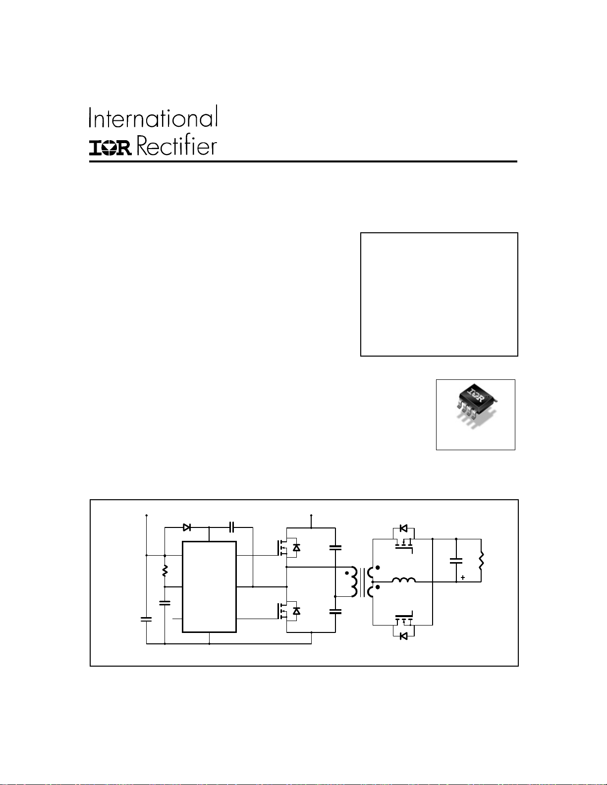
Vin
S
1
S
2
C
2
C
1
SO -8SO -8
T
S
R1
L
S
R2
R
C
V
o
Simplified Circuit Diagram
www.irf.com
1
Page 2
IR2085S & (PbF)
Absolute Maximum Ratings
Absolute maximum ratings indicate sustained limits beyond which damage to the device may occur. All voltage parameters are absolute voltages referenced to COM. All currents are defined positive into any lead. The thermal resistance
and power dissipation ratings are measured under board mounted and still air conditions.
Symbol Definition Min. Max. Units
V
b
V
CC
V
S
V
HO
V
LO
OSC OSC pin voltage -0.3 VCC + 0.3
V
CS
dVS/dt Allowable offset voltage slew rate -50 +50 V/ns
I
CC
P
D
Rth
JA
T
J
T
S
T
L
High side floating supply voltage -0.3 150
Low side supply voltage — 25
High side floating supply offset voltage Vb - 25 Vb + 0.3
High side floating output voltage Vb - 0.3 V
Low side output voltage -0.3 VCC + 0.3
Cs pin voltage -0.3 VCC + 0.3
Supply current — 20 mA
Package power dissipation
Thermal resistance, junction to ambient — 200 °C/W
Junction temperature -55 150
Storage temperature -55 150
Lead temperature (soldering, 10 seconds) — 300
— 1.0 W
b
+ 0.3
°C
V
Recommended Operating Conditions
For proper operation the device should be used within the recommended conditions.
Symbol Definition Min. Max. Units
Vb High side floating supply voltage Vdd -0.7 15
V
S
V
CC
I
CC
R
T
C
T
fosc(max) Operating frequency (per channel) — 500
T
J
Note1: Care should be taken to avoid output switching conditions where the Vs node flies inductively below ground by more
than 5V.
2
Steady state high side floating supply offset voltage -5 100
Supply voltage 10 15
Supply current (Note 2) — 5 mA
Timing resistor 10 100 KΩ
Timing capacitor 47 1000 pF
Junction temperature -40 125 °C
Vdc
KHz
www.irf.com
Page 3
IR2085S & (PbF)
Dynamic Electrical Characteristics
V
(VCC, VBS) = 12V, C
BIAS
Symbol Definition Min. Typ. Max. Units Test Conditions
t
t
fosc Per channel output frequency 500 — — KHz
tdt High/low output dead time 50 — —
t
dcs
PM High/low pulse width mismatch -25 — 25 VS = 0V ~ 100V
Turn-on rise time — 40 60
r
Turn-off fall time — 20 30
f
Overcurrent shut down delay — 200 — pulse on CS
Static Electrical Characteristics
V
(VCC, VBS) = 12V, C
BIAS
Symbol Definition Min. Typ. Max. Units Test Conditions
V
OH
V
OL
I
leak
I
QBS
I
QCC
V
CS+ Overcurrent shutdown threshold
V
CS- Overcurrent shutdown threshold
U
VCC+
U
VCC-
U
VBS+
U
VBS-
I
O+
I
O-
High level output voltage, (V
Low level output voltage — — 0.1
Offset supply leakage current — — 50
Quiescent VBS supply current — — 150
Quiescent VCC supply current — — 1.5 mA
Undervoltage positive going threshold 6.8 7.3 7.8
Undervoltage negative going threshold 6.3 6.8 7.3
High side undervoltage positive going threshold 6.8 7.3 7.8
High side undervoltage negative going threshold 6.3 6.8 7.3
Output high short circuit current — 1.0 —
Output low short circuit current — 1.0 —
= 1000 pF, and TA = 25°C unless otherwise specified.
LOAD
= 1000 pF and TA = 25°C unless otherwise specified.
LOAD
- VO) — — 1.5
BIAS
250 300 350 mV
150 200 250 mV
nsec
nsec
V
µA
V
A
VS = 0V
CT =100pF,
RT =10Kohm
www.irf.com
3
Page 4

IR2085S & (PbF)
Functional Block Diagrams
RT
OSC
CT
VCC
CS
GND
UVLO BIAS
OSC
BLOCK
+
OVC
-
VREF
(250mV)
SOFT
START
10PF
IR2085S
BLOCK
DIAGRAM
PULSE
STEERING
UVLO
AND
RS
LATCH
Vb
HO
VS
VCC
LO
Lead Definitions
Symbol Description
V
CC
GND Logic supply return
Vb High side floating supply
V
S
HO High side output
LO Low side output
CS Current sense input
OSC Oscillator pin
4
Logic supply
Floating supply return
Lead Assignments
8
IR2085S
VCC
Vb
HO
VS
7
6
54
www.irf.com
CS
1
2
OSC
3
GND
LO
Also available LEAD-FREE (PbF)
Page 5

IR2085S & (PbF)
(
)
)
500
450
400
350
300
250
200
Frequency (kHz )
150
100
50
0
10 20 30 40 50 60 70 80 90 100
C
= 470pF
T
RT
C
= 220pF
T
kohms
C
= 100pF
T
CT = 47pF
Fig. 1 Typical Output Frequency (-25oC to 125oC)
180
160
250
225
200
175
150
Time (ns)
125
100
75
50
10 20 30 40 50 60 70 80 90 100
RT (kohms
CT = 470pF
C
= 220pF
T
C
= 100pF
T
C
= 47pF
T
Fig. 2 Typical Dead Time (@25oC)
www.irf.com
140
120
Dead Time (ns)
100
DT(CT=100pF, RT=100k)
80
60
-40-20 0 20 406080100120
Tem perature
Fig. 3 Typical Dead Time vs Temperature
5
Page 6

IR2085S & (PbF)
Pin descriptions
Cs: The input pin to the overcurrent comparator.
Exceeding the overcurrent threshold value specified in “Static Electrical Parameters” Section will
terminate output pulses and start a new soft start
cycle as soon as the voltage on the pin reduce
below the threshold value.
OSC: The oscillator-programming pin. Only two
components are required to program the internal
oscillator frequency: a resistor connected between
the Vcc pin and the OSC pin, and a capacitor
connected from the OSC to GND. The approximate oscillator frequency is determined by the
following simple formula:
f
= 1 / (2 · RT · CT)
osc
Where frequency is in Hertz (Hz), RT resistance
in Ohms (W) and CT capacitance in Farads (F).
The recommended range of timing resistors is
between 10kW and 100KW and range of time capacitances is between 47pF and 470pF. The timing resistors less than 10Kohm should be avoided.
The value of the timing capacitor determines the
amount of dead time between the two output drivers: lower the CT,
Shorter the dead time and vice versa. It is not recommended to use a timing capacitor below 47pF,
For best performance, keep the time components
as close as possible to the IR2085S. Separated
ground and Vdd traces to the timing components
are encouraged.
GND: Signal ground and power ground for all functions. Due to high current and high frequency
operation, a low impedance circuit board ground
plane is highly recommended.
HO, LO: High side and low side gate drive pins.
The high and low side drivers can directly drive the
gate of a power MOSFET. The drivers are capable
of 1A peak source and sink currents. It is recommended that the high and low drive pins be very
close to the gates of the high side and low side
MOSFETs to prevent any delay and distortion of
the drive signals.
Vb: The high side power input connection. The
high side supply is derived from a bootstrap circuit using a low-leakage Schottky diode and a
ceramic capacitor. To prevent noise, the Schottky
diode and bypass capacitor should be very close
to the IR2085S.
Vs: The high side power return connection. Vs
should be connected directly to the source terminal of high side MOSFET with a trace as short as
possible.
Vcc: The IC bias input connection for the device.
Although the quiescent Vcc current is very low,
total supply current will be higher, depending on
the gate charge of the MOSFETs connected to
the HO and LO pins, and the programmed oscillator frequency, Total Vcc current is the sum of quiescent Vcc current and the average current at HO
and LO. Knowing the operating frequency and
the MOSFET gate charge (Qg) at selected Vcc
voltage, the average current can be calculated from
Iave = 2 x Qg X fosc
To prevent noise problem, a bypass ceramic capacitor connected to Vcc and GND should be
placed as close as possible to the IR2085S.
IR2085S has an under voltage lookout feature for
6
www.irf.com
Page 7

IR2085S & (PbF)
the IC bias supply, Vcc. The minimum voltage
required on Vcc to make sure that IC will work
within specifications must be higher than 8.5V
(9.5V minimum Vcc is recommended to prevent
asymmetrical gates signals on HO and LO pins
that are expected when Vcc is between 7.5V and
8.5V).
APPLICATION INFORMATION
An example of a half-bridge DC Bus Converter
designed for 150W wireless telecommunications,
networking, and high-end computing applications
is shown in Figure 4. This circuit operates at
220kHz and provides 20A of output current. At 48V
nominal input voltage, the output voltage is 8V.
On the primary side, the IR2085S drives two
IRF7493s - next generation low charge power
MOSFETs. The primary side bias is obtained
through a linear regulator from the input voltage for
startup, and then from the transformer in steady
state. The IRF7380, dual 80VN power MOSFET
in an SO8 package is used for the primary side
bias function.
parallel, while operating from different input
voltages, and also to allow continuing output current
if one of the two input sources is shorted or
disconnected.
Two ferrite cores are used for the transformer and
inductor. The transformer core is a PQ20/16 (3F3)
with 3:1 turns ratio and 1mil gap. The inductor
core is an E14/3.5/5 (3F3) with one turn and a
5mil gap. The PCB has eight layers, with two
layers for primary windings that are connected in
parallel and each has three turns. Four layers are
used for the secondary windings. Each layer has
one turn and two layers are connected in parallel
to get two sets of secondary windings. 4 oz Cu
PCB is recommended for the primary and
secondary windings. Each primary side winding
is placed between the two sets of the secondary
windings to balance the secondary side current.
On the secondary side, two IRF6612s - Novel
DirectFET power MOSFETs are used for self-driven
synchronous rectification. DirectFETs practically
eliminate MOSFET packaging resistance, which
maximizes circuit efficiency. The DirectFET
construction includes a copper “clip” across the
backside of the silicon, which enables top-sided
cooling and improved thermal performance. In the
circuit shown in Fig. 4, the DirectFET gate drive
voltage is clamped to an optimum value of 7.5V
with the IRF9956 dual SO-8 MOSFET. The
secondary side bias scheme is designed to allow
outputs of two bus converters to be connected in
www.irf.com
7
Page 8

IR2085S & (PbF)
Vdd
47
36 ~60V input
1u
IR2085S56 k
CS
OSC
GND
LO VC C
VB
HO
VS
20 0
20 0
39 k
3V
15 V
rm
IRF7 493
1u
Vdd
IRF7 380
39 k
.1u
9V
Vdd
36 ~60V input
3. 3u
1u
3. 3u
IRF7 493
Figure 4 – IR2085S DC Bus converter reference design.
IRF6 612
IRF6 612
.1u
10 0k
IRF9 956
10 k
10 k
22 u
22 u
6~10Vout
8
www.irf.com
Page 9

Case outline
IR2085S & (PbF)
A
E
D B
5
87
6
6X
0.25 [.010]
65
H
4312
0.25 [.010] A
e
8X b
e1
A1
A
CAB
NOTES:
1. DIMENS ION ING & TO LERAN CING P ER AS ME Y14.5M-1994.
2. C ONTROLLING DIMENSION: MILLIMETER
3. DIMENSIONS ARE SHOWN IN MILLIMETERS [INCHES].
4. OUTLINE CONFORMS TO JEDEC OUTLINE MS-012AA.
C
0.10 [.004]
6.46 [.255]
3X 1.27 [.050]
y
8-Lead SOIC
DIM
FOOTPRINT
8X 0.72 [.028]
8X 1.78 [.070]
MIN MAX
A
.0532
A1
b
c .0075 .0098 0.19 0.25
D
E
e
e1
H
K
L
y
.0688
.0040
.0098
.013
.020
.189
.1968
.1497
.1574
.050 BAS IC
.025 BA SIC 0.635 B ASIC
.2284
.2440
.0099
.0196
.016
.050
0°
K x 45°
8X L
8X c
7
5 DIMENSION DOES NOT INCLUDE MOLD PROTRUSIONS.
MOL D PR OTRU SIONS NOT TO EXC EED 0.15 [.006].
6 DIMENSION DOES NOT INCLUDE MOLD PROTRUSIONS.
MOL D PR OTRU SIONS NOT TO EXC EED 0.25 [.010].
7 DIMENSION IS THE LENGTH OF LEAD FOR SOLDERING TO
A SU BSTRA TE.
01-0021 11
8°
MILLIMETERSIN C H E S
MIN MAX
1.35
1.75
0.10
0.25
0.33
0.51
4.80
5.00
3.80
4.00
1.27 BAS IC
5.80
6.20
0.25
0.50
0.40
1.27
0°
8°
01-6027
(MS-012AA)
www.irf.com
9
Page 10

IR2085S & (PbF)
LEADFREE PART MARKING INFORMATION
PKG
DESIG
S
S
Part number
Date code
Pin 1
Identifier
?
MARKING CODE
Lead Free Released
P
Non-Lead Free
Released
IRxxxxxx
YWW?
ORDERING INFORMATION
PART LEADFREE
NUMBER PART NUMBER
IR2085S IR2085SPbF
IR2085STR IR2085STRPbF
?XXXX
(Prod mode - 4 digit SPN code)
Assembly site code
Per SCOP 200-002
PIN
COUNT
8
8
IR logo
Lot Code
PARTS
PER TUBE
95
------
PARTS
PER REEL
------
4000
10
This product has been designed and qualified for the industrial market.
Qualification Standards can be found on IR’s Web Site http://www.irf.com/.
Data and specifications subject to change without notice
WORLD HEADQUARTERS: 233 Kansas Street, El Segundo, California 90245 Tel: (310) 252-7105
1/7/2006
www.irf.com
 Loading...