

Page 1
Data sheet No. PD60279
IPS6011(S)(R)PbF
INTELLIGENT POWER HIGH SIDE SWITCH
Features
• Over temperature shutdown (with auto-restart)
• Short circuit protection (current limit)
• Reverse battery protection (turns On the MOSFET)
F is a five terminal Intelligent Power
• Full diagnostic capability (short circuit to battery)
• Active clamp
• Open load detection in On and Off state
• Ground loss protection
• Logic ground isolated from power ground
• ESD protection
Description
)PbThe IPS6011(S)(R
Switch (IPS) for use in a high side configuration. It features
short circuit, over-temperature, ESD protection, inductive
load capability and diagnostic feedback. The output
current is limited to the Ilim value. The current limitation is
activated until the thermal protection acts. The overtemperature protection turns off the device if the junction
temperature exceeds the Tshutdown value. It will
automatically restart after the junction has cooled 7°C
below the Tshutdown value. The reverse battery
protection turns On the MOSFET. A diagnostic pin
provides different voltage levels for each fault condition.
The double level shifter circuitry will allow large offsets
between the logic and load ground.
Product Summary
Rds(on) 14mΩ max.
Vclamp 39V
I Limit 60A
Open load 3V / 2.4A
Packages
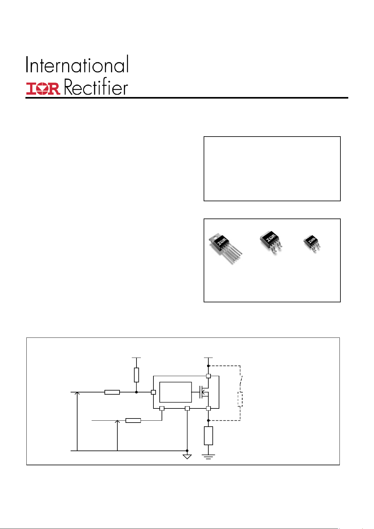
TO-220 D²Pak D-Pak
IPS6011PbF IPS6011SPbF IPS6011RPbF
Typical Connection
Out(5)
Control
Dg(4)
Rin
Vcc(3)
Load
+Bat
Input Signal
V Diag
In(2)
Gnd(1)
Rdgs
Pull-up resistors required for
open load off and short
circuit to Vbat detection
Rdgp
+5V
www.irf.com
1
Page 2
IPS6011(S)(R)PbF
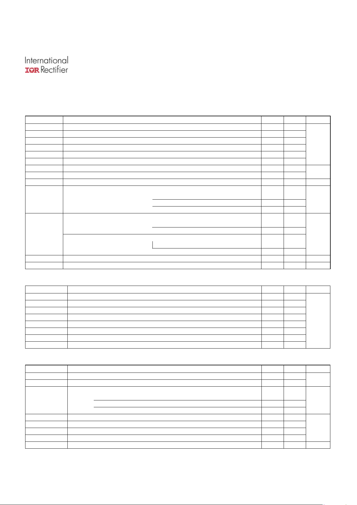
Absolute Maximum Ratings
Absolute maximum ratings indicate sustained limits beyond which damage to the device may occur. All voltage parameters
are referenced to Ground lead. (Tambient=25°C unless otherwise specified).
Symbol Parameter Min. Max. Units
Vout Maximum output voltage Vcc-35 Vcc+0.3
Voffset Maximum logic ground to load ground offset Vcc-35 Vcc+0.3
Vin Maximum input voltage -0.3 5.5
Vcc max. Maximum Vcc voltage
⎯
36
Vcc cont. Maximum continuous Vcc voltage
⎯
28
Vcc sc. Maximum Vcc voltage with short circuit protection
⎯
24
V
Iin max. Maximum IN current -3 10
Idg max. Maximum diagnostic output current -3 10
mA
Vdg Maximum diagnostic output voltage -0.3 5.5 V
Maximum power dissipation (internally limited by thermal protection)
Rth=5°C/W IPS6011
⎯
25
Rth=40°C/W IPS6011S 1”sqrt. footprint
⎯
3.1
Pd
Rth=50°C/W IPS6011R 1”sqrt. footprint
⎯
2.5
W
Electrostatic discharge voltage (Human body) C=100pF, R=1500Ω
Between In and Vcc
⎯
1500
Other combinations
⎯
4000
Electrostatic discharge voltage (Machine Model) C=200pF,R=0Ω,L=10µH
Between In and Vcc
⎯
100
ESD
Other combinations
⎯
500
V
Tj max. Max. storage & operating temperature junction temperature -40 150 °C
Tsoldering Soldering temperature (10 seconds)
⎯
300 °C
Thermal Characteristics
Symbol Parameter Typ. Max. Units
Rth1 Thermal resistance junction to ambient IPS6011 TO220 free air 50
⎯
Rth2 Thermal resistance junction to case IPS6011 TO220 1.2
⎯
Rth1 Thermal resistance junction to ambient IPS6011S D²Pak std. footprint 60
⎯
Rth2 Thermal resistance junction to ambient IPS6011S D²Pak 1” sqrt. footprint 40
⎯
Rth3 Thermal resistance junction to case IPS6011S D²Pak 1.2
⎯
Rth1 Thermal resistance junction to ambient IPS6011R D-Pak std. footprint 70
⎯
Rth2 Thermal resistance junction to ambient IPS6011R D-Pak 1” sqrt. footprint 50
⎯
Rth3 Thermal resistance junction to case IPS6011R D-Pak 1.2
⎯
°C/W
Recommended Operating Conditions
These values are given for a quick design. For operation outside these conditions, please consult the application notes.
Symbol Parameter Min. Max. Units
VIH High level input voltage 4 5.5
VIL Low level input voltage 0 0.9
Continuous drain current, Tambient=85°C, Tj=125°C, Vin=5V
Rth=5°C/W IPS6011
⎯
18
Rth=40°C/W IPS6011S 1” sqrt. footprint
⎯
6.3
Iout
Rth=50°C/W IPS6011R 1” sqrt. footprint
⎯
5.6
A
Rin Recommended resistor in series with IN pin 4 10
Rdgs Recommended resistor in series with DG pin for reverse battery protection 4 20
Rdgp Recommended pull-up resistor for DG 4 20
Rol Recommended pull-up resistor for open load detection 5 100
kΩ
F max. Max. switching frequency
⎯
0.3 kHz
www.irf.com
2
Page 3
IPS6011(S)(R)PbF
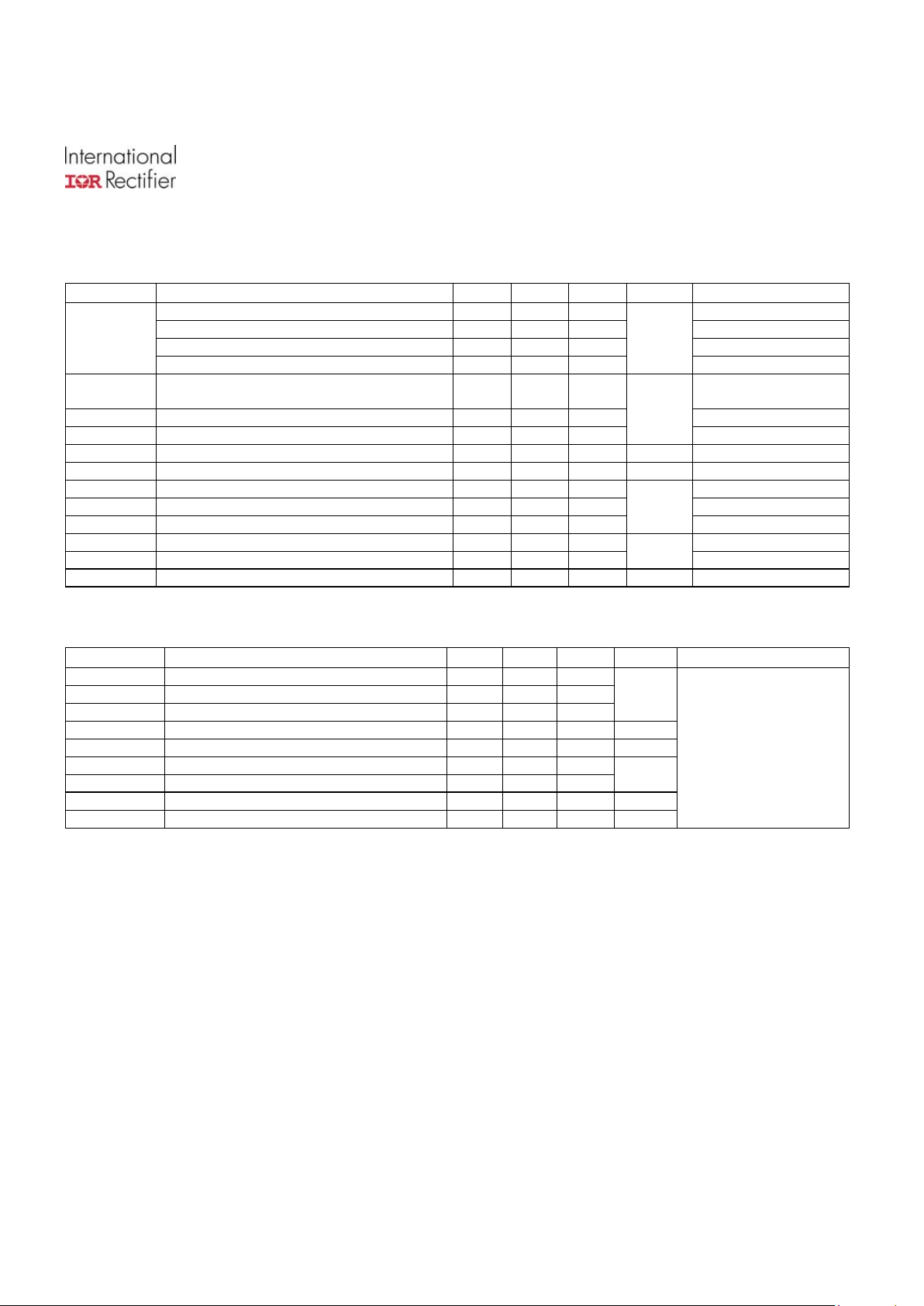
Static Electrical Characteristics
Max. Units Test Conditions
Tj=25°C, Vcc=14V (unless otherwise specified)
Symbol Parameter Min. Typ.
ON state resistance Tj=25°C
⎯
11 14 5 2Vin= V, Iout= 0A
ON state resistance Tj=150°C
⎯
19.5 25 0A Vin=5V, Iout=2
O
⎯
12 17 0A N state resistance Tj=25°C, Vcc=6V Vin=5V, Iout=2
Rds(on)
ON state resistance during reverse battery
⎯
15 20
mΩ
-Gn V Vcc d=14
Vcc op. Operating voltage range with short circuit
p
6
⎯
24
rotection
V clamp 1 V 39
⎯
=50m
cc to Out clamp voltage 1 37
Iout A
V clamp 2 Vcc to Out clamp voltage 2
⎯
40 42
V
=16A FigIout (see . 1)
Icc Off S
⎯
4 9 µA =0V t=0V
upply current when Off
Vin , Vou
Icc On S
⎯
2.2 5 mA 5V
upply current when On
Vin=
Vih I
nput high threshold voltage
⎯
2.5 2.9
Vil Input low threshold voltage
⎯
1.5 2
In hyst. Input hysteresis
V
0.2 0.5 1
Iin On Input current when device is On =5V
⎯
40 100 Vin
Idg D g=5V g leakage current
⎯
0.1 10
µA
Vd
Vdg Low level DG voltage 5 0.4 V =1.
⎯
0.2 Idg 6mA
Sw ching
Vcc=14V, Resistive load=1Ω, Vin=5V, Tj=25°C
Max. Units T Conditions
it Electrical Characteristics
Symbol Parameter Min. Typ. est
Tdon Turn-on delay time
⎯
30 60
Tr1 Rise time to Vout=Vcc-5V
⎯
25 50
Tr2 Rise time to Vout=0.9 x Vcc
⎯
40 100
µs
dV/dt (On) Turn On dV/dt
⎯
0.3 0.8 V/µs
EOn Turn On energy
⎯
4
⎯
mJ
Tdoff Turn-off delay time
⎯
70 140
Tf F
80
µs
all time to Vout=0.1 x Vcc
⎯
30
dV/dt (Off) T
µs
urn Off dV/dt
⎯
0.7 2 V/
EOff T.urn Off energy
⎯
1.5
⎯
mJ
see Fig 3
www.irf.com
3
Page 4
IPS6011(S)(R)PbF
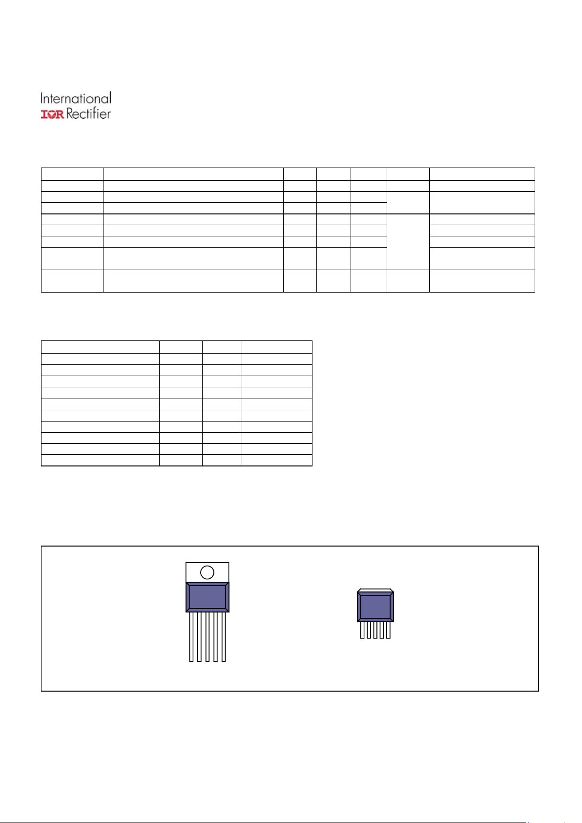
Protection Characteristics
Symbol Parameter Min. Typ. Max. Units Test Conditions
Ilim Internal current limit V35 60 85 A out=0V
Tsd+ Over temperature high threshold 150(1) 16⎯5
Tsd-
1
⎯
°C S
Over temperature low threshold
⎯
58
ee fig. 2
Vsc 3 4 Short-circuit detection voltage(2) 2
UV
5 5.9
⎯
UV hyst. 0.25
⎯
1.6
VOL Off detection threshold 2 3 4
V
Open load
I OL On Open load detection threshold 0 1 2 A .5 .6 .4
( nteed
(2) Reference
T abl
ting C DG
1) Guara by design
to Vcc
rue T e
Opera onditions IN OUT
Normal H H H
Normal L H L
Open Load H H L
Open Load (3) L H L
Short circuit to Gnd H L L
Short circuit to L L H Gnd
Short circuit to H L (4) Vcc H
Short circuit to L Vcc (5) L H
Over-temperat L ure H L
Over-temperat L L H ure
(3) With a pull-up resistor connected between the output and Vcc.
(4) Vds lower tha
( ithout a pul
ead Assignments
n 10mV.
5) W l-up resistor connected between the output and Vcc.
L
1 2 3 4 5
TO220
1- Gnd
2- In
3- Vcc
4- Dg
5- Out
3- Vcc
1 2 3 4 5
D²Pak – D Pak
3- Vcc
www.irf.com
4
Page 5
IPS6011(S)(R)PbF
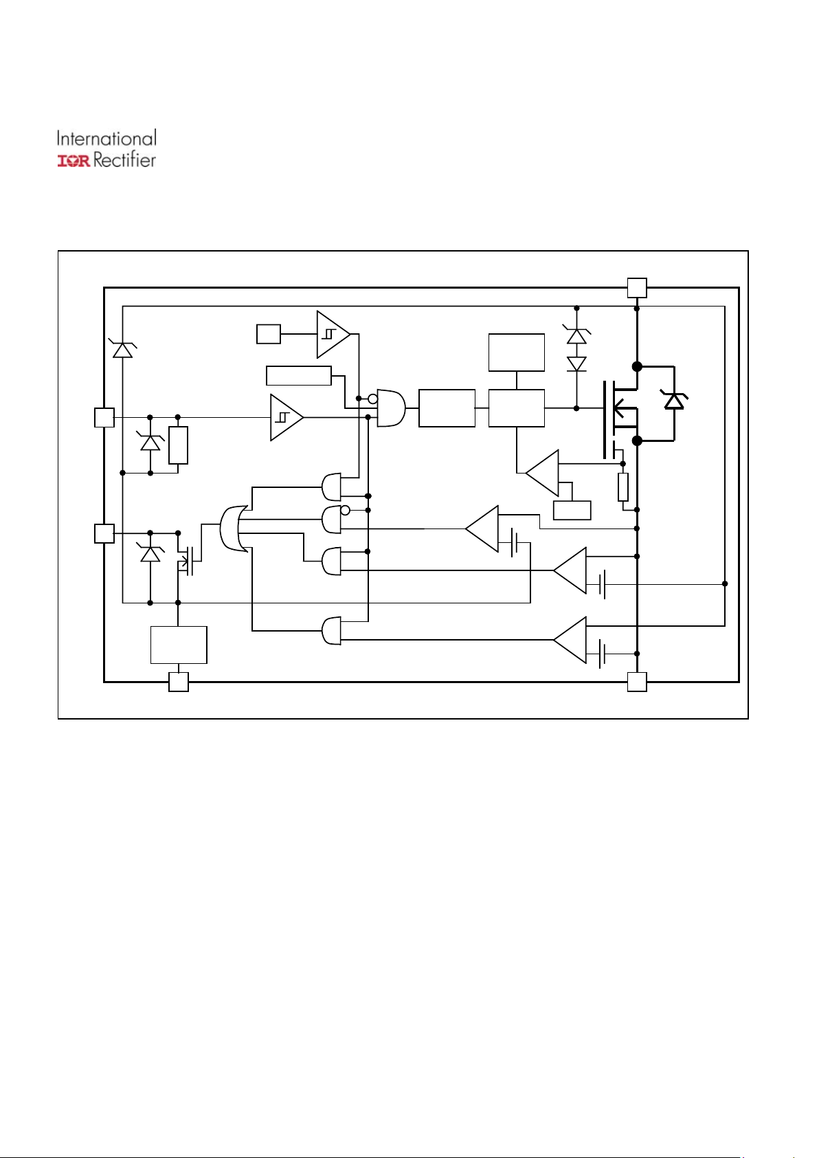
Functional Block Diagram
All values are typical
IN
V
CC
OUT
37V
Driver
I Limit
43V
150k
I sense
-
+
CPuharge
mp
Level
Shifter
Tj
165°C
158°C
Ω
2.5V
2.0V
6V
DG
6V
GND
Ground
nnect Disco
3V
-
+
Open load
ver-te
20mV
off
O mp
-
+
Open load on
3V
-
+
Short circuit
43V
Vcc-gnd >UV
www.irf.com
5
Page 6
IPS6011(S)(R)PbF
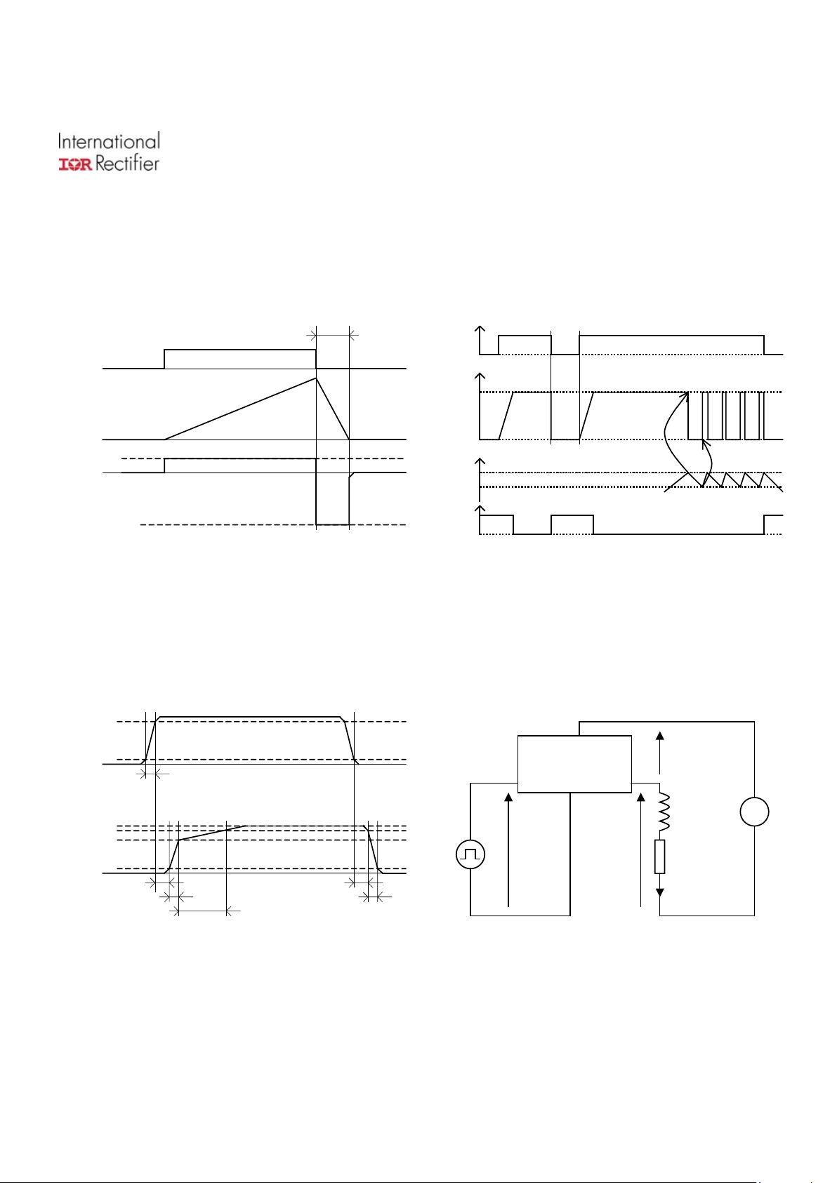
Vds
Ids
Vin
Vcc
Vds clamp
T clamp
See Application Notes to evaluate power di ssipat ion
T
j
Ilim
Tsd+
Tsd-
Iout
Vin
limiting Thermal cycling
DG
Figure 1 – Active clamp waveforms Figure 2 – Protection timing diagram
Vout
Vin
Tr-in
90%
10%
90%
10%
Td on
Tr1
Td off
Tf
Vcc-5V
Tr2
Vcc
Figure 3 – Switching times definitions Figure 4 – Active clamp test circuit
Vclam
p
Iout
Vin
In
Vcc
Out
R
L
0V
5V
14V
+
-
Vout
Rem :
During active
clamp, Vload
is negative
D
g
Gnd
www.irf.com
6
Page 7
IPS6011(S)(R)PbF
4000
50%
100%
150%
-50 0 50 100 150
200%
0
5
10
15
20
25
30
-50 0 50 100 1 50
35
40
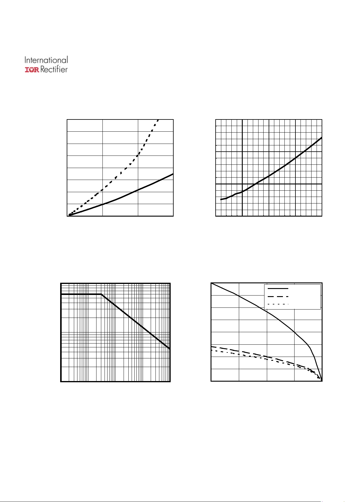
TO220 5°C/W
D2Pak 40°C/W
DPak 50°C/W
Fig ut
current (A)
Iout, Output current (A)
ure 5 – Switching energy (µJ) Vs Outp
Eon, Eoff, switching energy (µJ)
0
1000
2000
3000
0 5 10 15
1
10
0.001 0.01 0.1 1 10
100
Tj, junction temperature (°C)
Fig C)
Rds(on), Drain-to-Source On Resistance
(Normalized)
Fi d
inductance (mH)
Load inductance (mH)
Iout, Output current (A)
Vs Ambient temperature (°C)
Ids, cont. Output current (A)
Tamb, Ambient temperature (°C)
Eon
Eoff
ure 6 - Normalized Rds(on) (%) Vs Tj (°
gure 7 – Max. Output current (A) Vs Loa Figure 8 – Max. ouput current (A)
www.irf.com
7
Page 8
IPS6011(S)(R)PbF
www.irf.com
8
0.01
0.1
1
10
100
1e-5 1e-4 1e-3 1e-2 1e-1 1e+0 1e+1 1e+2 1e+3
0
10
20
30
40
50
60
70
80
-50 0 50 100
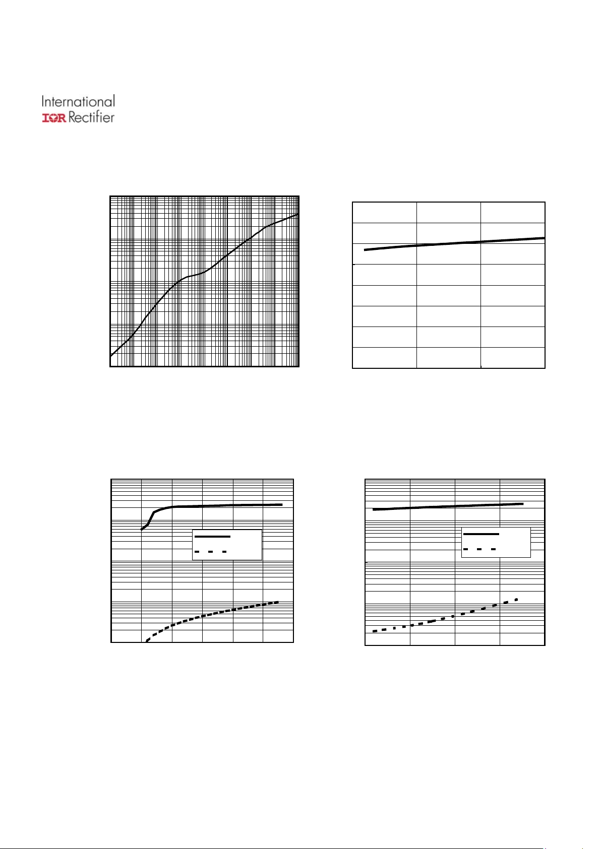
Figure 10 –I limit (A)
Vs junction temperature (°C)
Vcc V)
Figure 9 – Transient thermal impedance (°C/W)
°C)
Zth, transient thermal impedance (°C/W)
I limit (A)
Time (s) Tj, junction temperature (
Vs time (s)
1.E+0
1.E+1
1.E+2
1.E+3
1.E+4
0 5 10 15 20 25 30
Icc on
Icc off
1.E+0
1.E+1
1.E+2
1.E+3
1.E+4
-50 0 50 100 150
Icc on
Icc off
Icc on/ Icc off, supply current (µA)
Icc on/ Icc off, supply current (µA)
Tj, junction temperature (°C)
, power supply voltage (
Figure 11 – Icc on/ Icc off (µA) Vs Vcc (V) Fig C) ure 12 – Icc on/ Icc off (µA) Vs Tj (°
Page 9
IPS6011(S)(R)PbF
www.irf.com
9
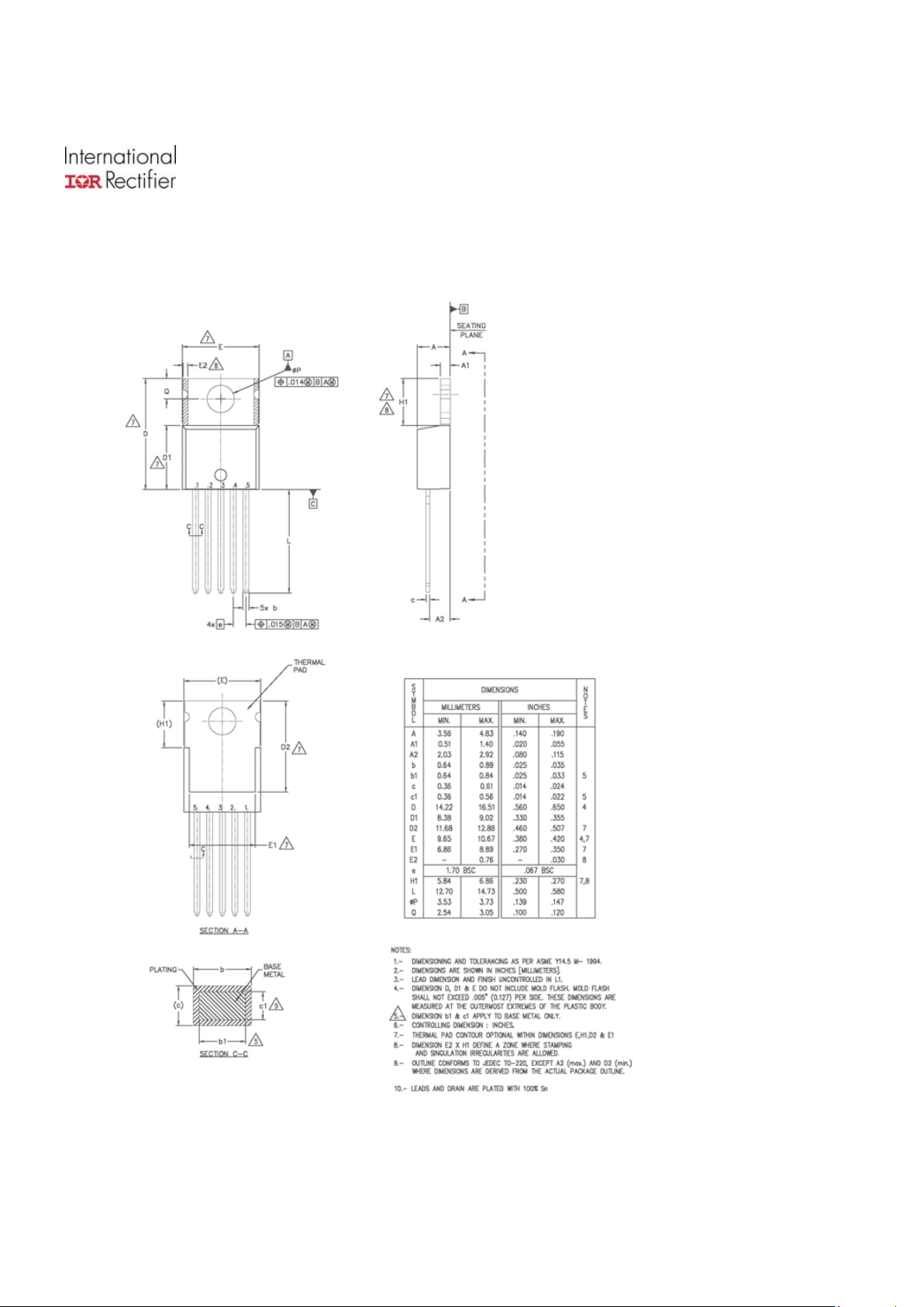
Case Outline - TO220 (5 lead) - Automotive Q100 PbF qualified
Page 10
IPS6011(S)(R)PbF
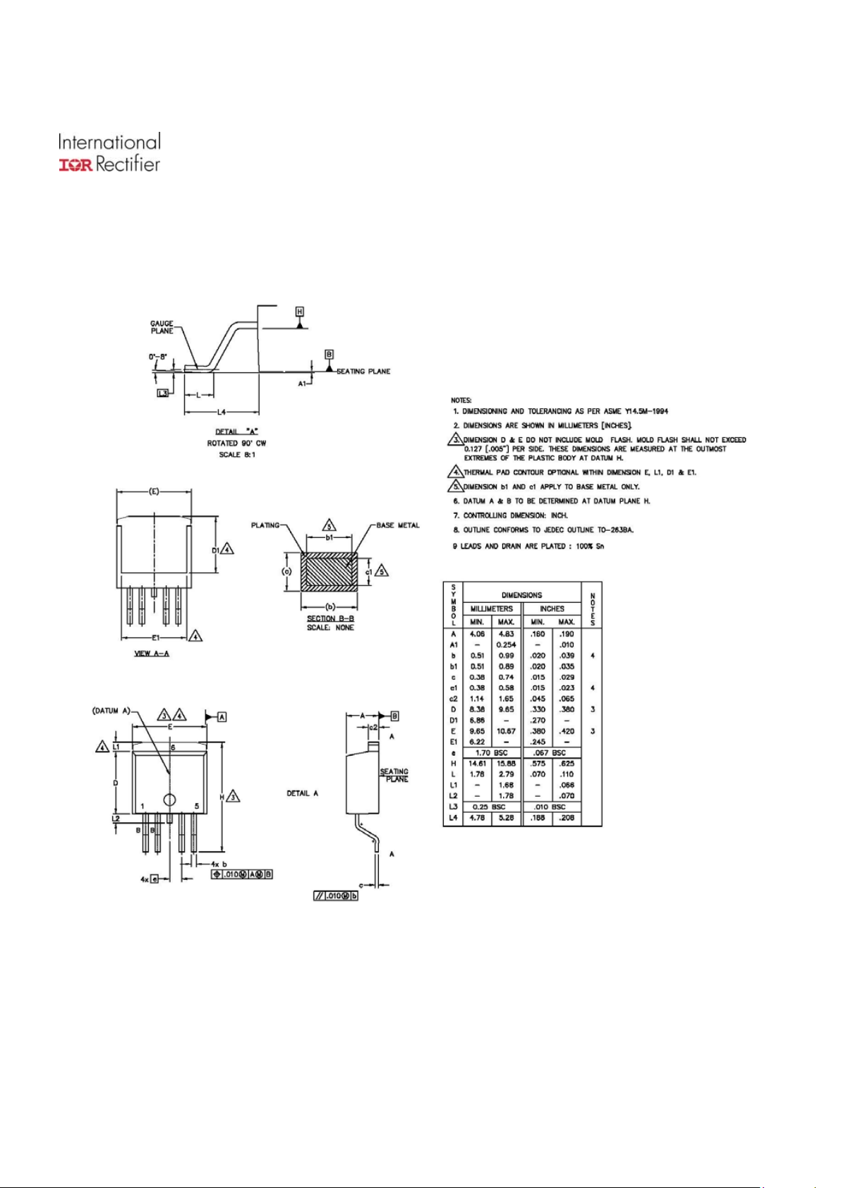
Case Outline 5 Lead - D2PAK - Automotive Q100 PbF MSL1 qualified
www.irf.com
10
Page 11
IPS6011(S)(R)PbF
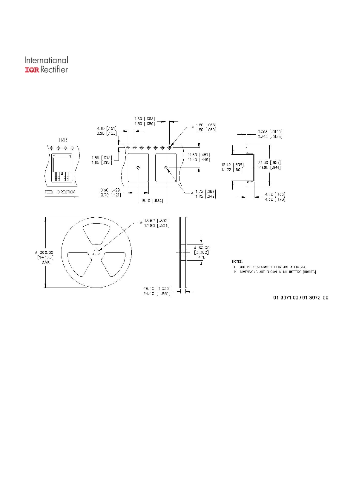
Tape & Reel 5 Lead - D2PAK
www.irf.com
11
Page 12
IPS6011(S)(R)PbF
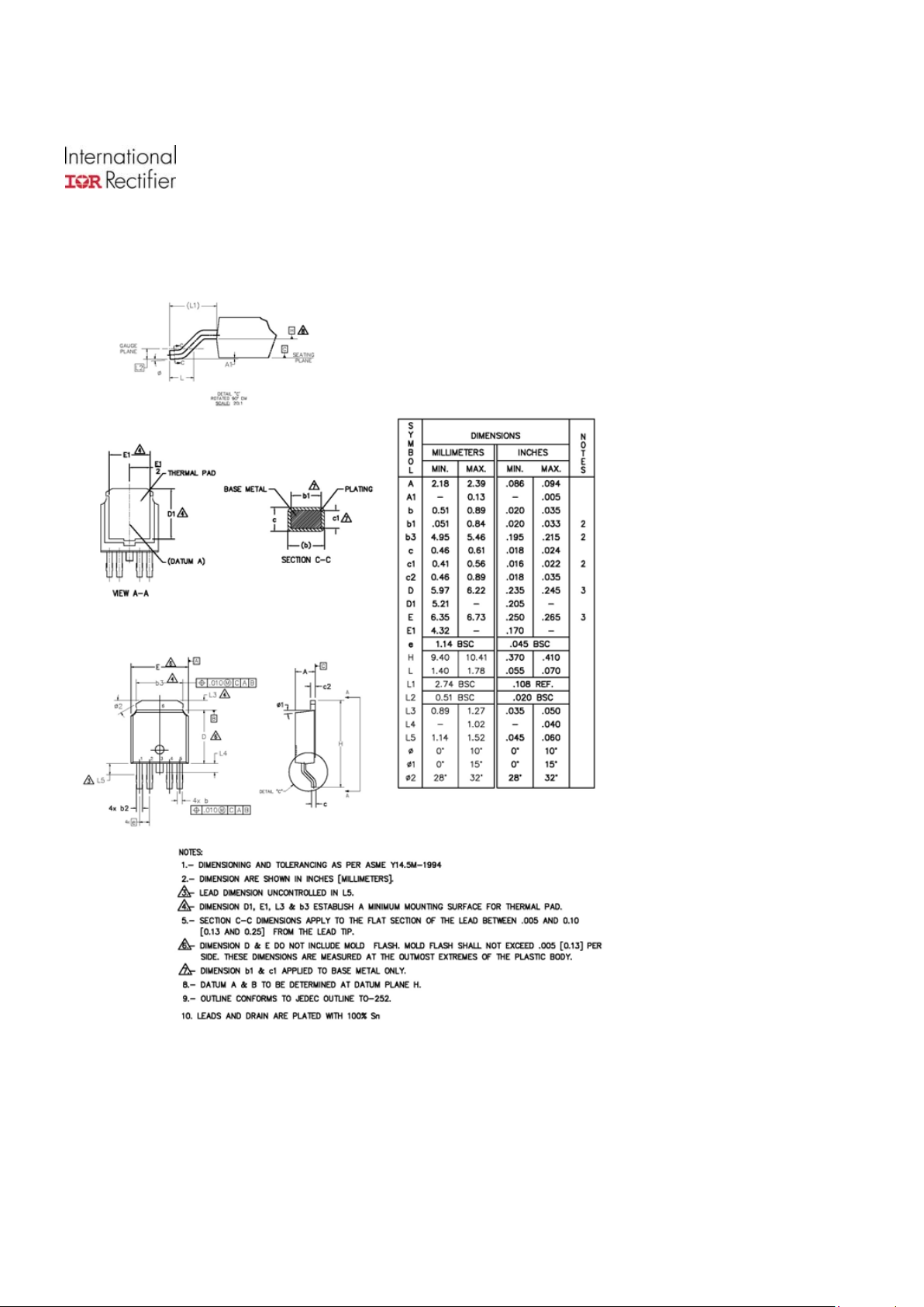
Case Outline 5 Lead – DPAK - Automotive Q100 PbF MSL1 qualified
www.irf.com
12
Page 13
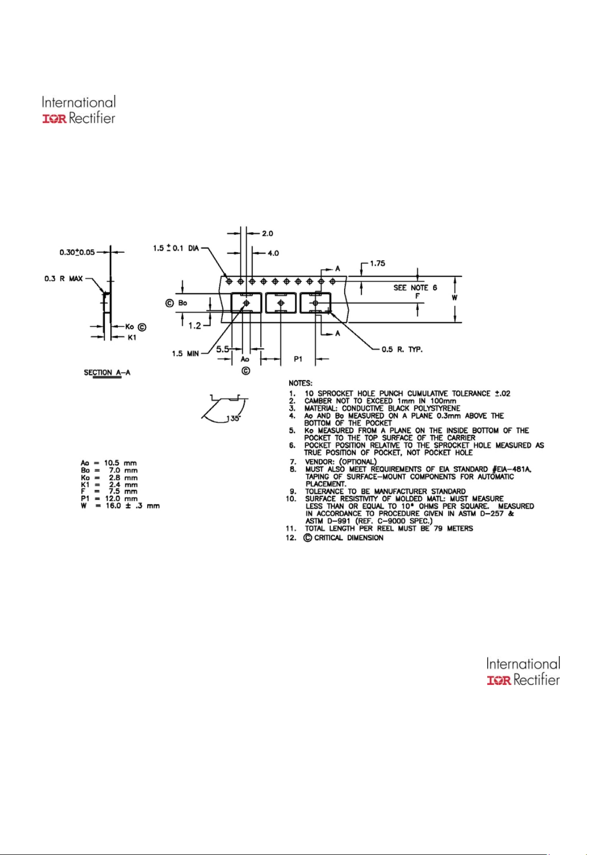
IPS6011(S)(R)PbF
Tape & Reel 5 Lead – DPAK
IR WORLD HEADQUARTERS: 233 Kansas St., El Segundo, California 90245 Tel: (310) 252-7105
Data and specifications subject to change without notice.
TO220, D2Pak and Dpak is MSL1 qualified.
This product has been designed and qualified for the Automotive [Q100] market. 11/25/2006
www.irf.com
13
 Loading...