

Page 1
Data Sheet No.PD 60151-J
IPS031G/IPS032G
SINGLE/DUAL FULLY PROTECTED POWER MOSFET SWITCH
Features
• Over temperature shutdown
• Over current shutdown
• Active clamp
• Low current & logic level input
• E.S.D protection
Description
The IPS031G/IPS032G are fully protected single/dual
low side SMART POWER MOSFETs that feature overcurrent, over-temperature, ESD protection and drain
to source active clamp.These devices combine a
HEXFET® POWER MOSFET and a gate driver. They
offer full protection and high reliability required in
harsh environments. The driver allows short switching times and provides efficient protection by turning
off the power MOSFET when the temperature exceeds 165
The device restarts once the input is cycled. The
avalanche capability is significantly enhanced by the
active clamp and covers most inductive load demagnetizations.
o
C or when the drain current reaches 12A.
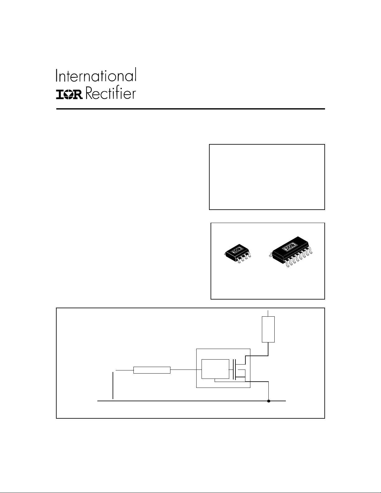
Typical Connection
Product Summary
R
ds(on)
V
clamp
Ishutdown 12A
T
on/Toff
Packages
8-Lead SOIC
IPS031G
70mΩ (max)
50V
1.5µs
16-Lead SOIC
IPS032G
(Dual)
Load
R in series
(if needed)
Q
Logic signal
(Refer to lead assignment for correct pin assignment)
www.irf.com 1
IN
control
S
D
S
Page 2
31
IPS031G/IPS032G
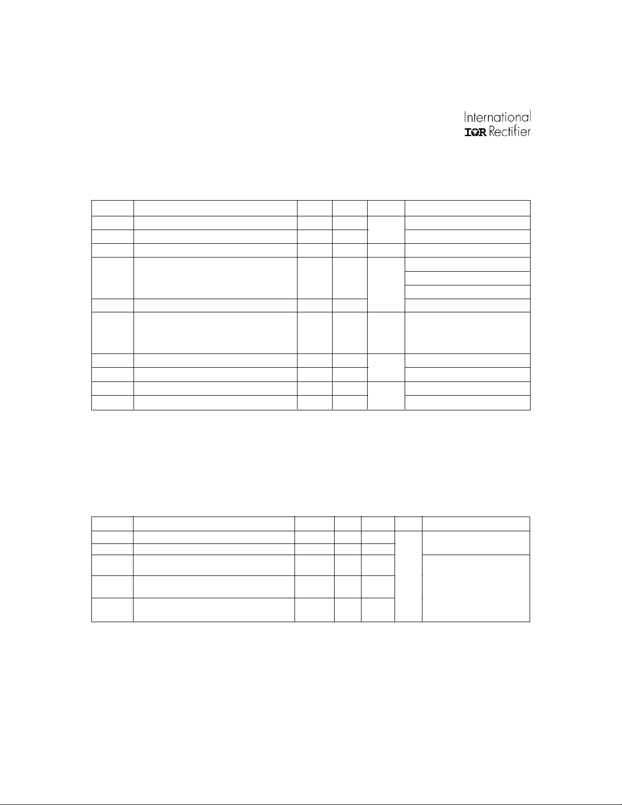
Absolute Maximum Ratings
Absolute maximum ratings indicate sustained limits beyond which damage to the device may occur. All voltage parameters are referenced to SOURCE lead. (T
copper thickness. All Sources leads of each mosfet must be connected together to get full current capability
Symbol Parameter Min. Max. Units Test Conditions
V
ds
V
in
I
in, max
I
sd cont.
I
sd pulsed
P
d Maximum power dissipation
ESD1 Electrostatic discharge voltage (Human Body) — 4 C=100pF, R=1500Ω,
ESD2 Electrostatic discharge voltage (Machine Model) — 0.5 C=200pF, R=0Ω, L=10µH
T
stor.
T
j
Maximum drain to source voltage — 47
Maximum input voltage -0.3 7
Maximum IN current -10 +10 mA
Diode max. continuous current
(rth=125oC/W) IPS031G — 1 .4
(for all sd mosfets, rth=85
Diode max. pulsed current
(rth=125oC/W) IPS031G — 1 W
(for all Pd mosfets, rth=85
Max. storage temperature -55
max. Max. junction temperature -40
= 25oC unless otherwise specified). PCB mounting uses the standard footprint with 70 µm
Ambient
V
(1)
o
C/W) IPS032G — 2
(1)
(for ea. mosfet)
(1)
o
C/W) IPS032G — 1 .5
—15
150
150
A
kV
o
C
Thermal Chacteristics
Symbol Parameter Min. T yp. Max. Units Test Conditions
R
th1
R
th2
R
th1
(2 mos on) (2 mosfets on) — 85
R
th2
(1 mos on) (1 mosfet on) — 100 —
R
th3
(2 mos on) (2 mosfets on) — 60 —
(1) Limited by junction temperature (pulsed current limited also by internal wiring)
Thermal resistance with standard footprint
Thermal resistance with 1" square footprint —
Thermal resistance with standard footprint
Thermal resistance with standard footprint
Thermal resistance with 1" square footprint
—
100
65
2 www.irf.com
—
—
—
o
C/W
SOIC-8
SOIC-16
Page 3
IPS031G/IPS032G
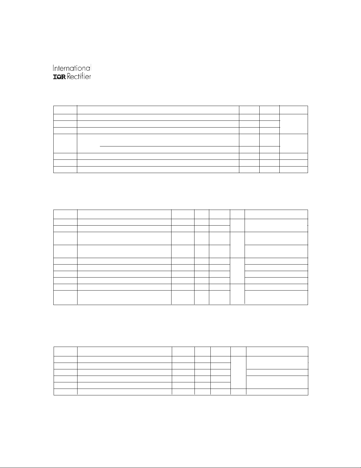
Recommended Operating Conditions
These values are given for a quick design. For operation outside these conditions, please consult the application notes.
Symbol Parameter Min. Max. Units
Vds
V
IH
V
IL
I
ds
Tamb=85oC (
R
in
T
r-in(max)
Fr-I
Static Electrical Characteristics
(Tj = 25oC unless otherwise specified.)
Symbol Parameter Min. Typ. Max. Units Test Conditions
R
ds(on)
R
ds(on)
I
dss
@Tj=25oC
I
dss2
@Tj=25oC
V clamp 1
V clamp 2 Drain to source clamp voltage 2 50
V
in clamp
V
th
I
in, -on
I
in, -off
Continuous Drain to Source voltage
(max)
High level input voltage 4 6
Low level input voltage
Continuous drain current
TAmbient = 85
(
Recommended resistor in series with IN pin 0.2
Max recommended rise time for IN signal (see fig. 2) — 1 µS
(2)
Max. frequency in short circuit condition (Vcc = 14V) 0 1 kHz
sc
ON state resistance Tj = 25oC 204560
ON state resistance Tj = 150oC—75
Drain to source leakage current 0 0.5 25 Vcc = 14V, Tj = 25oC
Drain to source leakage current 0 5 50 Vcc = 40V, Tj = 25oC
Drain to source clamp voltage 1
IN to source clamp voltage
IN threshold voltage 1 1.6 2
ON state IN positive current
OFF state IN positive current
TAmbient = 85oC, IN = 5V, rth = 85oC/W, Tj = 125oC) IPS032G — 1.65
o
C, IN = 5V, rth = 100oC/W, Tj = 125oC) IPS031G — 2.2 A
100
47 52
53 60
7 8.1 9.5
25 90
50 130
56
200 Vin = 5V
250 Vin = 5V
—
0 0.5
Vin = 5V, Ids = 1A
mΩ
µA
Id
= 20mA (see Fig.3 & 4)
Id=I
V
µA
shutdown
I
= 1 mA
in
I
= 50mA, Vds = 14V
d
over-current triggered
35
V
5 k
Ω
(see Fig.3 & 4)
Switching Electrical Characteristics
V
= 14V, Resistive Load = 5Ω (IPS031), Resistive Load = 3Ω (IPS031S), Rinput = 50Ω, 100µs pulse,Tj = 25oC, (unless
cc
otherwise specified).
Symbol Parameter Min. Typ. Max. Units Test Conditions
T
on
T
r
T
rf
T
off
T
f
Q
in
www.irf.com 3
Turn-on delay time
Rise time
Time to 130% final R
Turn-off delay time
Fall time
Total gate charge
ds(on)
0.05
0.4
—
0.8
0.5
—
0.3
1
8
2
1.5
1.1
0.6
2
—
3.5
2.5
—
See figure 2
µ
s
See figure 2
nC Vin = 5V
Page 4
IPS031G/IPS032G
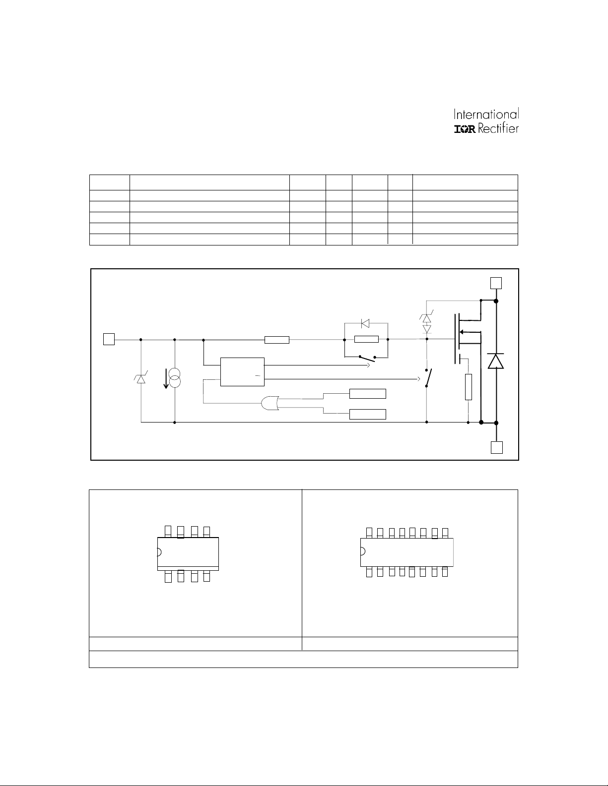
Protection Characteristics
Symbol Parameter Min. Typ. Max. Units Test Conditions
T
sd
I
sd
V
reset
T
reset
EOI_OT Short circuit energy (see application note)
Over temperature threshold — 165 —
Over current threshold 10 14 18 A See fig. 1
IN protection reset threshold 1. 5 2.3 3 V
Time to reset protection
—
10
2
40
400
Functional Block Diagram
All values are typical
300
Ω
200 k
o
C See fig. 1
µs Vin = 0V, Tj = 25oC
µJVcc = 14V
—
DRAIN
47 V
Ω
IN
8.1 V
µ
80
A
Lead Assignments
D D D D
1
S S S In
8 Lead SOIC
IPS031G
S
R
Q
Q
T > 165°c
I > 1sd
I sense
SOURCE
D1
D1 D1 D1 D2 D2 D2 D2
1
S1 S1 S1 I1 S2 S2 S2 I2
16 Lead SOIC
(Dual)
IPS032G
Part Number
4 www.irf.com
Page 5
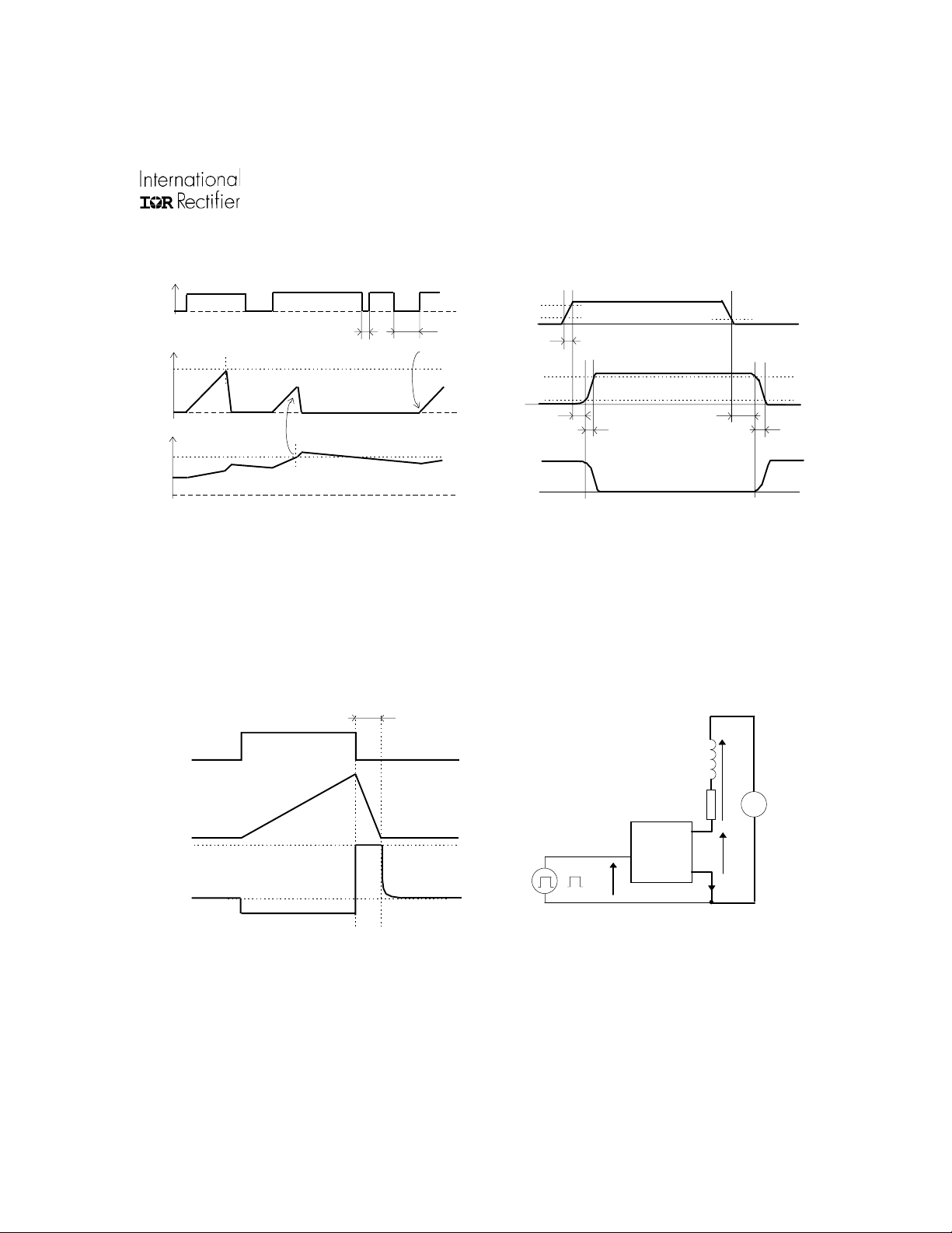
Vin
p
p
(
)
Ids
Isd
T
Tsd
(165 °c)
IPS031G/IPS032G
5 V
0 V
t < T reset
I shutdown
T shutdown
t > T reset
90 %
10 %
10 %
90 %
Tr-in
Tr-in
Td on
tr
Td off
tf
Figure 1 - Timing diagram
Vds clam
Vcc
( see Appl . Notes to evaluate power dissipation )
Figure 3 - Active clamp waveforms
T clam
Figure 2 - IN rise time & switching time definitions
L
V load
Rem : V load is negative
during demagnetization
Vin
5 v
0 v
R
D
IN
S
+
14 V
-
Figure 4 - Active clamp test circuit
www.irf.com 5
Page 6
IPS031G/IPS032G
All curves are typical values with standard footprints. Operating in the shaded area is not recommended.
100
90
80
70
60
50
40
30
20
10
0
012345678
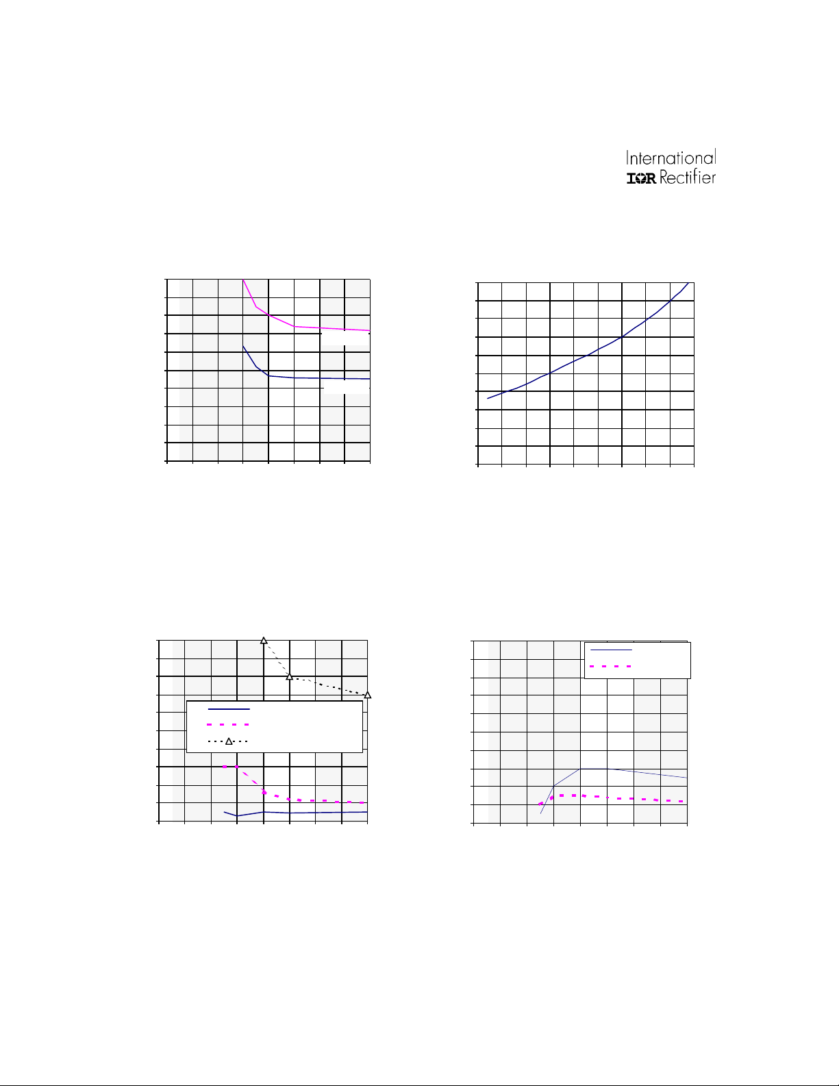
Figure 5 - Rds ON (mΩ) Vs Input Voltage (V)
10
9
8
7
6
5
4
3
2
1
0
012345678
ton delay
rise time
130% final r dson
Tj = 150oC
Tj = 25oC
200%
180%
160%
140%
120%
100%
80%
60%
40%
20%
0%
-50 -25 0 25 50 75 100 125 150 175
Figure 6 - Normalised Rds ON (%) Vs Tj (oC)
10
9
8
7
6
5
4
3
2
1
0
012345678
toff delay
fall time
Figure 7 - Turn-ON Delay Time, Rise Time &
Time to 130% final Rds(on) (us) Vs Input Voltage
(V)
Figure 8 - Turn-OFF Delay Time & Fall Time (us)
Vs Input Voltage (V)
6 www.irf.com
Page 7
IPS031G/IPS032G
100
delay on
rise time
130% rdson
10
1
0.1
10 100 1000 10000
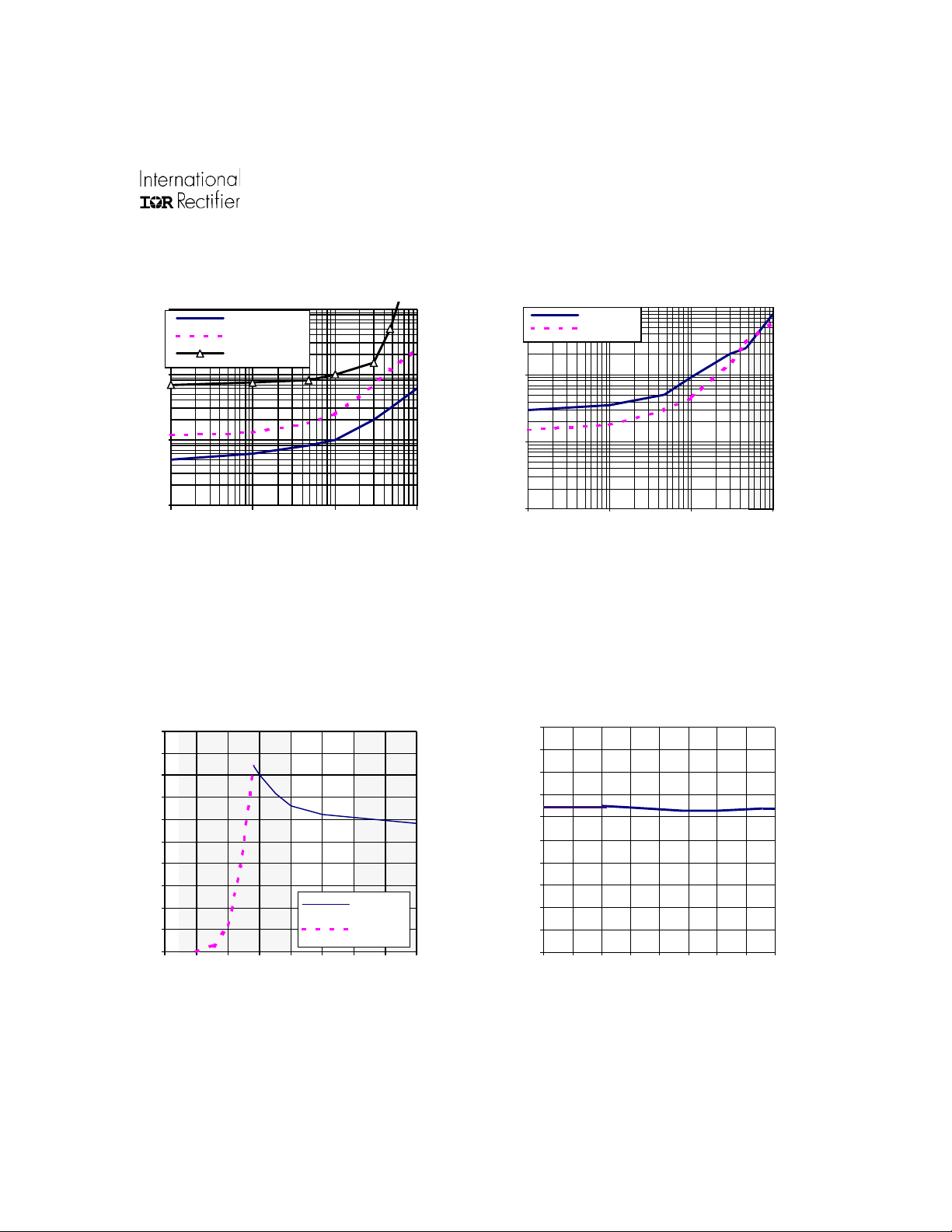
Figure 9 - Turn-ON Delay Time, Rise Time &
Time to 130% final Rds(on) Vs IN Resistor (Ω)
20
18
16
14
12
10
8
6
4
2
Isd 25°C
Ilim 25°C
0
012345678
100
delay off
fall time
10
1
0.1
10 100 1000 10000
Figure 10 - Turn-OFF Delay Time & Fall Time (us)
Vs IN Resistor (Ω)
20
18
16
14
12
10
8
6
4
2
0
-50 -25 0 25 50 75 100 125 150
Figure 12 - I shutdown (A) Vs Temperature (oC)Figure 11 - Current Iimimitation & I shutdown (A)
Vs Vin (V)
www.irf.com 7
Page 8
IPS031G/IPS032G
10
8
6
4
2
0
-50 0 50 100 150 200
Vs Amb. Temperature (oC) - IPS031G
100
rth = 5 0°C/W
SO8 Std. footprint 100°C/W
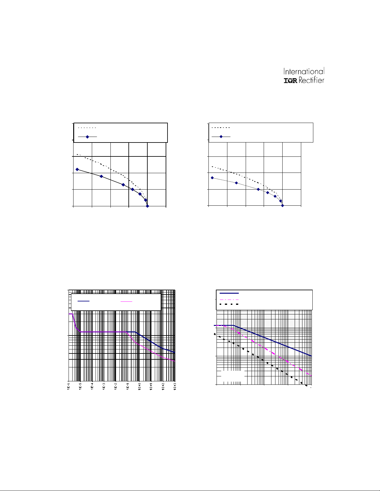
Figure 13a - Max.Cont. Ids (A)
T = 2 5 °C T = 100 °C
10
8
6
4
2
0
-50 0 50 100 150 200
SO16 Std. footprint 1 m osfe t on
SO8 Std. footprint 2 mosfets on
Figure 13b - Max.Cont. Ids (A)
Vs Amb. Temperature (oC) - IPS032G
single pulse
100
100 Hz rth=100°C /W dT=25 °C
1kHz rth=100°C/ W dT=25 °C
10
10
1
Vbat = 14 V
1
Figure 14 - Ids (A) Vs Protection Resp. Time (s)
IPS031G/IPS032G
Tjini = T s d
0.1
0.01 0.1 1 10 100
Figure 15 - Iclamp (A) Vs Inductive Load (mH)
8 www.irf.com
Page 9
IPS031G/IPS032G
100
rth SO8 std footprint
10
1
Single pulse
0.1
0.01
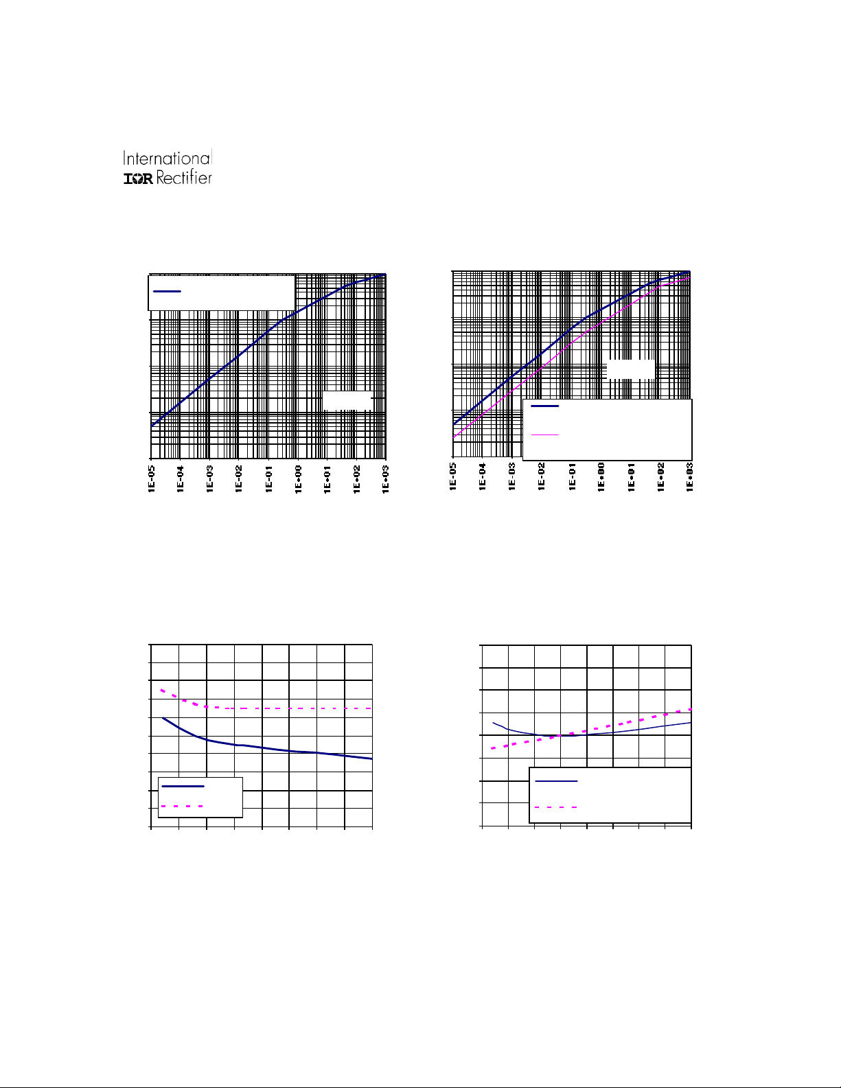
Figure 16a - Transient Thermal Imped. (oC/W)
Vs Time (s) - IPS031G
200
180
160
140
120
100
80
60
40
20
Iin,on
Iin,off
0
-50 -25 0 25 50 75 100 125 150
100
10
0.1
1
rth SO16 std footprint 1
Single pulse
mosfet active
rth SO16 std footprint 2
0.01
mosfets active
Figure 16b - Transient Thermal Imped. (oC/W)
Vs Time (s) - IPS032G
120%
115%
110%
105%
100%
95%
90%
85%
Vds clamp @ Isd
Vi n clamp @ 10mA
80%
-50 -25 0 25 50 75 100 125 150
Figure 17 - Input current (µA) Vs Tj (oC)
Figure 18 - Vin clamp and V clamp2 (%)
Vs Tj (oC)
www.irf.com 9
Page 10
IPS031G/IPS032G
16
14
12
Treset
rise time
fall time
10
8
6
4
2
0
-50 -25 0 25 50 75 100 125 150
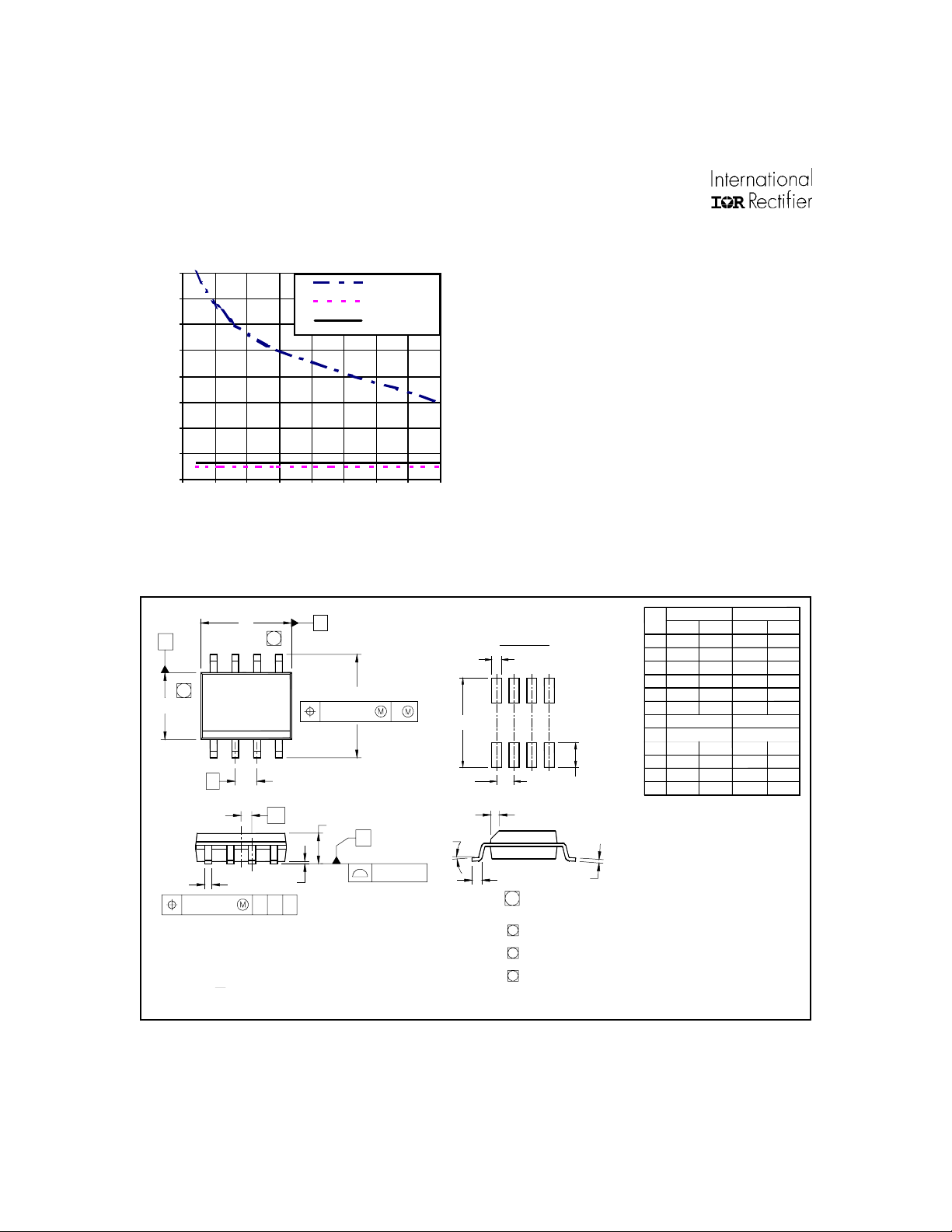
Figure 19 - Turn-on, Turn-off, and Treset KI
Vs Tj (oC)
Case Outlines
D B
A
87
6
E
e
6X
5
65
4312
H
0.25 [.010] A
6.46 [.255]
3X 1.27 [.050]
FOOTPRINT
8X 0.72 [.028]
8X 1.78 [.070]
.0688
.0098
.020
.1968
.1574
.2440
.0196
.050
8°
MILLIMET ERSINCHES
MIN MAX
1.35
0.10
0.33
4.80
3.80
1.27 BASIC
5.80
0.25
0.40
0°
DIM
MIN MAX
.0532
A
.0040
A1
.013
b
c .0075 .0098 0.19 0.25
.189
D
.1497
E
.050 BASIC
e
.025 BASIC 0.635 BASIC
e1
.2284
H
.0099
K
.016
L
0°
y
1.75
0.25
0.51
5.00
4.00
6.20
0.50
1.27
8°
e1
A
C
8X b
A1
0.25 [.010] C A B
NOTES :
1. DIMENSIONING & T OLERANCING PER ASME Y14.5M-1994.
2. CONTROLLING DIMENSION: MILLIMETER
3. DIMENS IONS ARE S HOWN IN MILLIMET E R S [INCHES ].
4. OUTLINE CONFORMS TO JEDEC OUTLINE MS-012AA.
y
0.10 [.004]
8-Lead SOIC
K x 45 °
8X L
8X c
7
5 DIMENS ION DOES NOT INCLUDE MOLD PR OTRUS IONS .
MOLD PROTRUSIONS NOT TO EXCEED 0.15 [.006].
6 DIMENS ION DOES NOT INCLUDE MOLD PR OTRUS IONS .
MOLD PROTRUSIONS NOT TO EXCEED 0.25 [.010].
7 DIMENSION IS THE LENGTH OF LEAD FOR SOLDERING TO
A SUBSTRATE.
01-0021 11
01-6027
(MS-012AA)
10 www.irf.com
Page 11
IPS031G/IPS032G
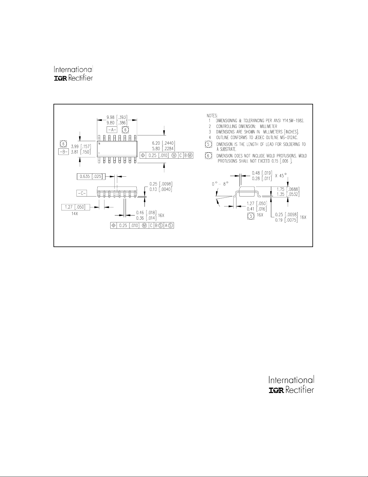
16 -Lead SOIC (narrow body)
IR WORLD HEADQUARTERS: 233 Kansas St., El Segundo, California 90245 Tel: (310) 252-7105
Data and specifications subject to change without notice. 6/11/2001
01-3064 00 (MS-012AC)
01-6018
www.irf.com 11
 Loading...