

Page 1
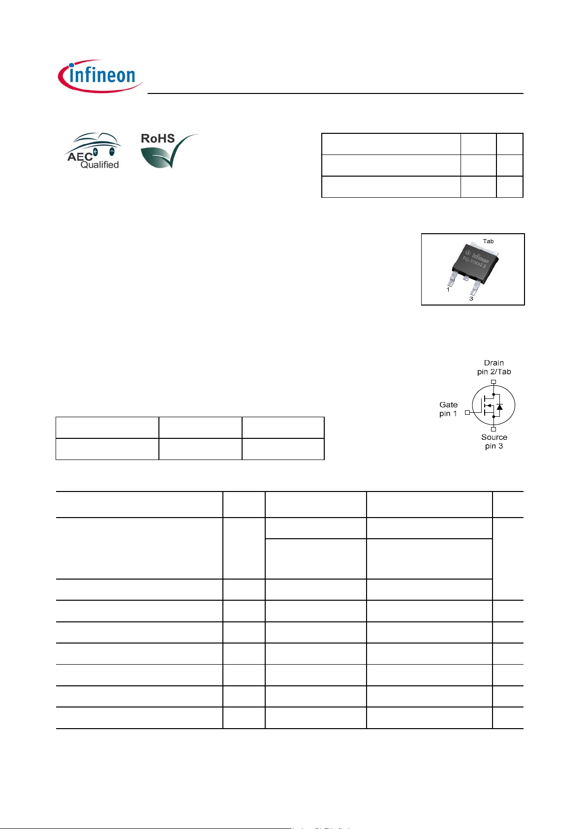
IPD90N06S4-04
OptiMOS®-T2 Power-Transistor
Features
• N-channel - Enhancement mode
• AEC qualified
• MSL1 up to 260°C peak reflow
• 175°C operating temperature
• Green Product (RoHS compliant)
• 100% Avalanche tested
Product Summary
V
DS
R
DS(on),max
I
D
60 V
3.8
90 A
PG-TO252-3-11
mΩ
Type Package Marking
IPD90N06S4-04 PG-TO252-3-11 4N0604
Maximum ratings, at T
Parameter Symbol Conditions Unit
Continuous drain current
Pulsed drain current
Avalanche energy, single pulse
Avalanche current, single pulse
Gate source voltage
Power dissipation
Operating and storage temperature
=25 °C, unless otherwise specified
j
1)
I
D
TC=25°C, VGS=10V
T
2)
2)
I
D,pulse
E
AS
I
AS
V
GS
P
tot
T
, T
j
TC=25°C
ID=45A
-
- ±20 V
TC=25°C
- -55 ... +175 °C
stg
=100°C, VGS=10V
C
2)
90
Value
90 A
360
331 mJ
90 A
150 W
IEC climatic category; DIN IEC 68-1 - - 55/175/56
Rev. 1.2 page 1 2009-07-01
Page 2

IPD90N06S4-04
Parameter Symbol Conditions Unit
Values
min. typ. max.
Thermal characteristics
Thermal resistance, junction - case
Thermal resistance, junction ambient, leaded
SMD version, device on PCB
Electrical characteristics, at T
2)
R
thJC
R
thJA
R
thJA
=25 °C, unless otherwise specified
j
- - - 1.0 K/W
---62
minimal footprint - - 62
6 cm
2
cooling area
3)
--40
Static characteristics
Drain-source breakdown voltage
Gate threshold voltage
V
(BR)DSSVGS
V
GS(th)
=0V, ID= 1mA
VDS=VGS, ID=90µA
60 - - V
2.0 3.0 4.0
Zero gate voltage drain current
Gate-source leakage current
Drain-source on-state resistance
I
I
R
DSS
GSS
DS(on)
VDS=60V, VGS=0V,
T
=25°C
j
V
=60V, VGS=0V,
DS
T
=125°C
j
2)
VGS=20V, VDS=0V
VGS=10V, ID=90A
- 0.03 1 µA
- 10 100
- - 100 nA
- 3.2 3.8
mΩ
Rev. 1.2 page 2 2009-07-01
Page 3

IPD90N06S4-04
y
g
Parameter Symbol Conditions Unit
Values
min. typ. max.
namic characteristics
D
Input capacitance
Output capacitance
Reverse transfer capacitance
Turn-on delay time
Rise time
Turn-off delay time
Fall time
Gate Char
e Characteristics
Gate to source charge
Gate to drain charge
Gate charge total
2)
C
iss
V
=0 V, VDS=25 V,
C
oss
C
rss
t
d(on)
t
r
t
d(off)
t
f
2)
Q
gs
Q
gd
Q
g
GS
f =1 MHz
V
=30V, VGS=10V,
DD
I
=90A, R
D
V
DD
V
GS
G
=48V, ID=90A,
=0 to 10V
=3.5Ω
- 7980 10400 pF
- 1960 2540
- 75 150
-30-ns
-70-
-40-
-5-
-4457nC
-1020
- 99 128
Gate plateau voltage
V
plateau
- 5.4 - V
Reverse Diode
Diode continous forward current
I
S
- - 90 A
2)
TC=25°C
Diode pulse current
2)
Diode forward voltage
Reverse recovery time
Reverse recovery charge
1)
Current is limited by bondwire; with an R
2)
Defined by design. Not subject to production test.
3)
Device on 40 mm x 40 mm x 1.5 mm epoxy PCB FR4 with 6 cm2 (one layer, 70 µm thick) copper area for drain
connection. PCB is vertical in still air.
2)
2)
I
S,pulse
V
t
rr
Q
thJC
SD
rr
VGS=0V, IF=90A,
T
=25°C
j
VR=30V, IF=50A,
di
/dt =100A/µs
F
= 1.0K/W the chip is able to carry 152A at 25°C.
- - 360
0.6 0.95 1.3 V
- 125 - ns
- 110 - nC
Rev. 1.2 page 3 2009-07-01
Page 4
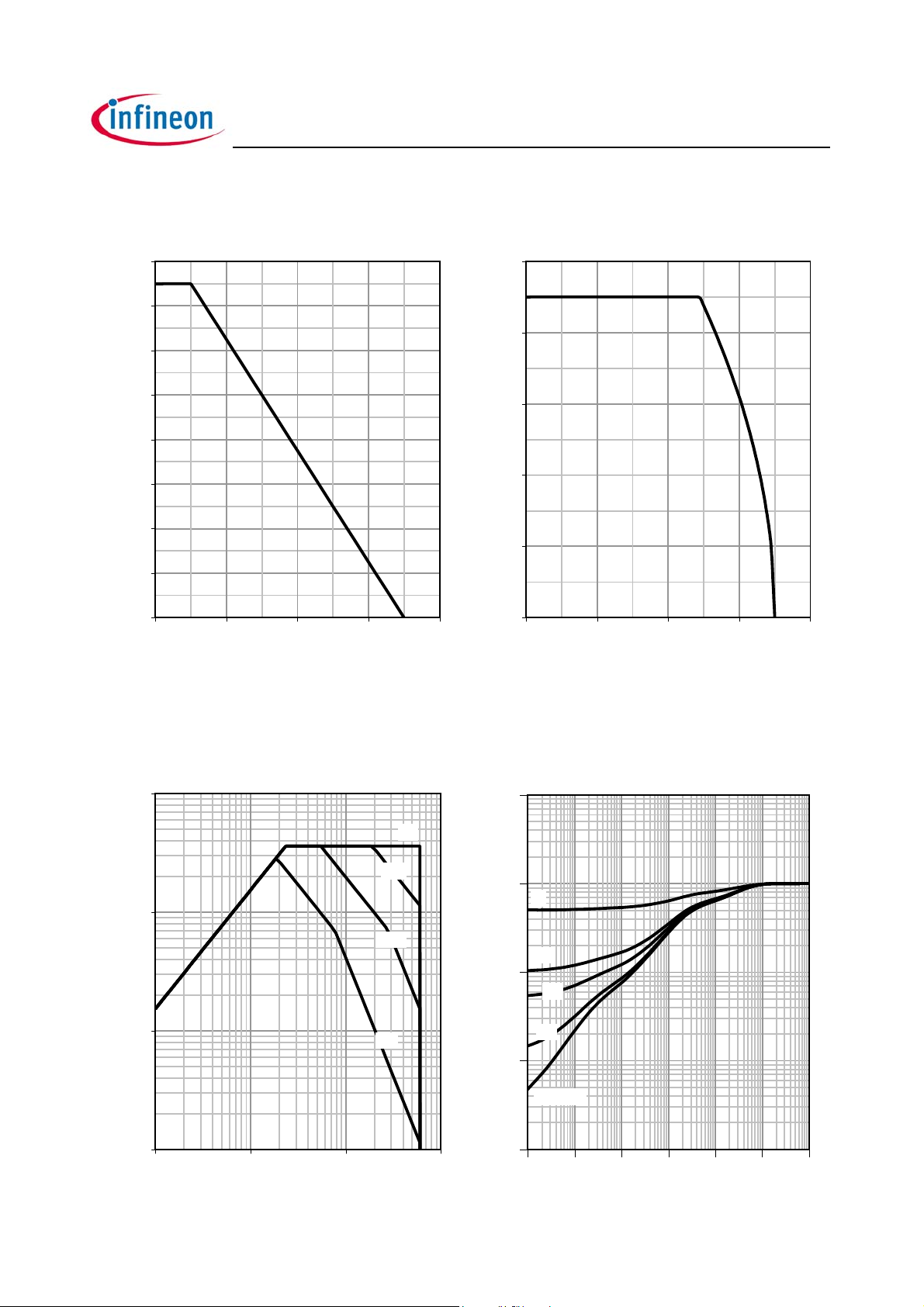
1 Power dissipation 2 Drain current
P
= f(TC); V
tot
≥ 6 V ID = f(TC); V
GS
GS
IPD90N06S4-04
≥ 6 V
160
100
140
80
120
100
[W]
tot
P
80
60
[A]
D
I
60
40
40
20
20
0
0 50 100 150 200
TC [°C]
0
0 50 100 150 200
TC [°C]
3 Safe operating area 4 Max. transient thermal impedance
I
= f(VDS); TC = 25 °C; D = 0 Z
D
parameter: t
p
1000
1 µs
10 µs
100
100 µs
[A]
D
I
10
1 ms
1
0.1 1 10 100
VDS [V]
= f(tp)
thJC
parameter: D =tp/T
1
10
0
10
0.5
0.1
-1
[K/W]
10
-2
-3
10
0.05
0.01
single pulse
-6
10
-5
thJC
Z
10
10
10
10
-3
-4
10
-2
10
-1
10
0
tp [s]
Rev. 1.2 page 4 2009-07-01
Page 5
IPD90N06S4-04
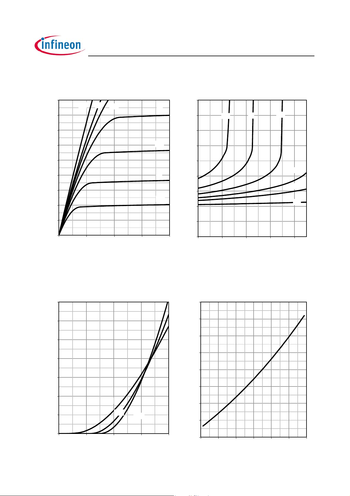
5 Typ. output characteristics 6 Typ. drain-source on-state resistance
I
= f(VDS); Tj = 25 °C R
D
parameter: V
GS
parameter: V
= f(ID); Tj = 25 °C
DS(on)
GS
360
10 V
8 V
7.5 V
7 V
320
280
240
6.5 V
200
[A]
D
I
160
6 V
120
5.5 V
80
40
0
01234
VDS [V]
10
9
5.5 V
6 V
8
7
]
Ω
6
[m
5
DS(on)
R
4
3
2
1
0 80 160 240 320
ID [A]
6.5 V
7 Typ. transfer characteristics 8 Typ. drain-source on-state resistance
7 V
7.5 V
10 V
I
= f(VGS); V
D
parameter: T
350
300
250
200
[A]
D
I
150
100
50
0
34567
= 6V R
DS
j
175 °C
25 °C
-55 °C
VGS [V]
= f(Tj); ID = 90 A; V
DS(on)
GS
= 10 V
6
5.5
5
4.5
]
Ω
[m
4
DS(on)
R
3.5
3
2.5
2
-60 -20 20 60 100 140 180
Tj [°C]
Rev. 1.2 page 5 2009-07-01
Page 6
IPD90N06S4-04
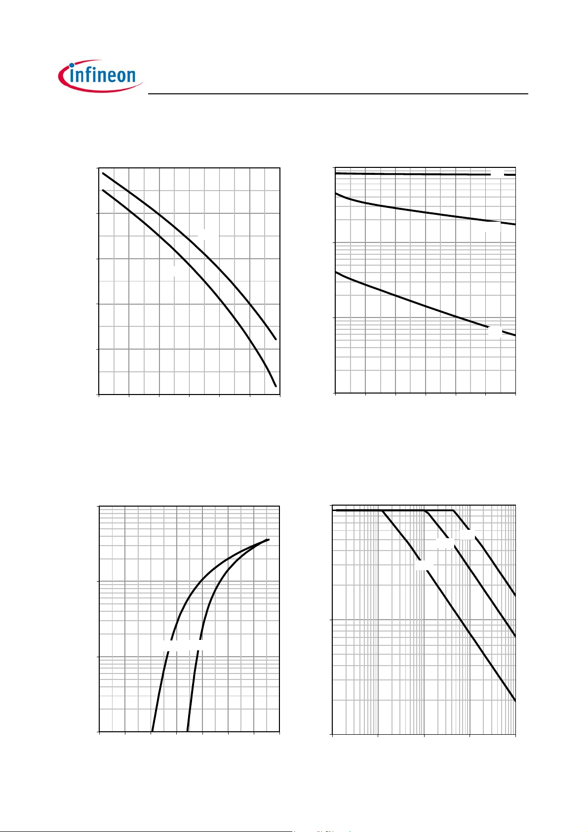
9 Typ. gate threshold voltage 10 Typ. capacitances
V
GS(th)
= f(Tj); V
parameter: I
4
3.5
3
[V]
GS(th)
V
2.5
2
1.5
-60 -20 20 60 100 140 180
= V
GS
DS
D
900 µA
C = f(VDS); V
4
10
3
10
= 0 V; f = 1 MHz
GS
Ciss
Coss
C [pF]
90 µA
2
10
Crss
1
10
0 5 10 15 20 25 30
Tj [°C]
VDS [V]
11 Typical forward diode characteristicis 12 Avalanche characteristics
IF = f(V
parameter: T
) I
SD
j
3
3
10
10
2
2
10
10
[A]
[A]
F
F
I
I
25 °C
25 °C
175 °C
1
1
10
10
0
0
10
10
0 0.2 0.4 0.6 0.8 1 1.2 1.4
0 0.2 0.4 0.6 0.8 1 1.2 1.4
175 °C
VSD [V]
VSD [V]
= f(tAV)
A S
parameter: T
100
[A]
10
AV
I
1
0.1 1 10 100 1000
j(start)
150 °C
tAV [µs]
25 °C
100 °C
Rev. 1.2 page 6 2009-07-01
Page 7
IPD90N06S4-04
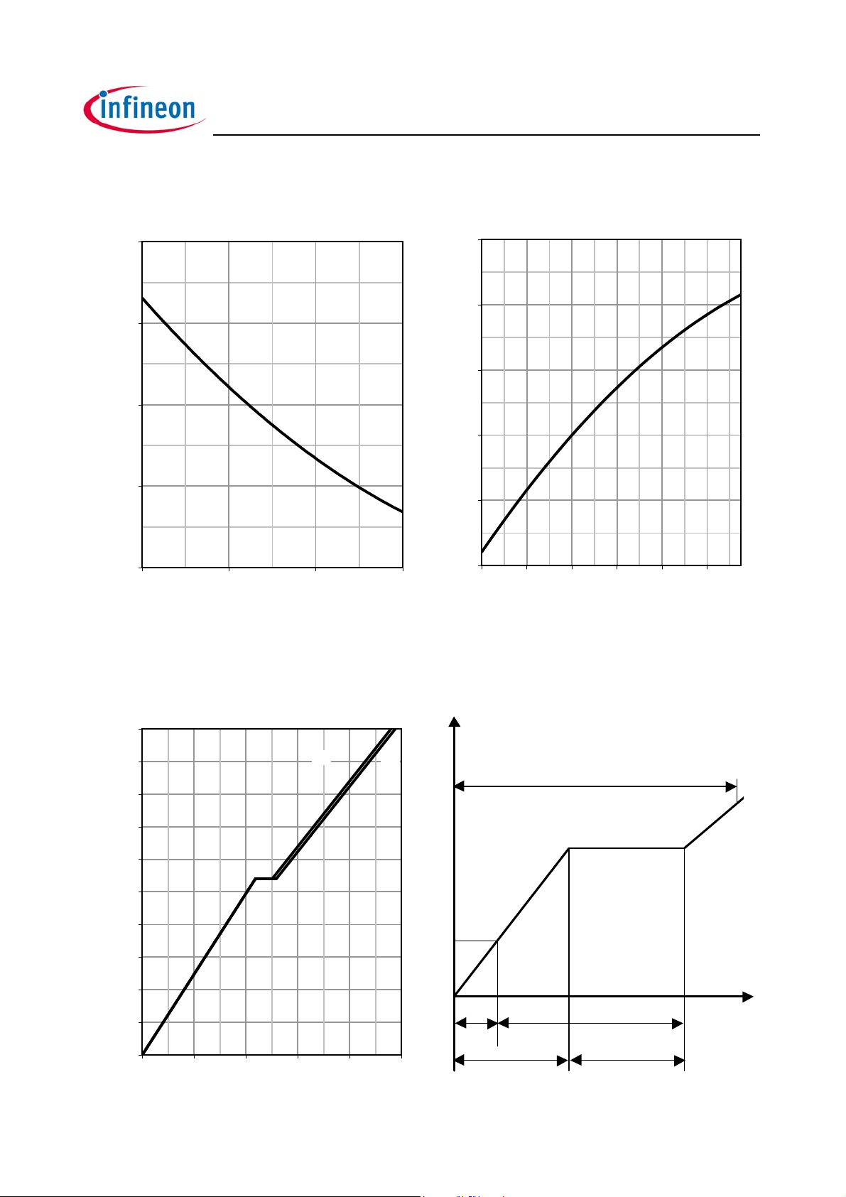
13 Avalanche energy 14 Drain-source breakdown voltage
E
= f(Tj); ID = 45 A V
AS
= f(Tj); ID = 1 mA
BR(DSS)
400
300
66
64
62
[V]
200
[mJ]
AS
E
100
0
25 75 125 175
BR(DSS)
V
60
58
56
-55 -15 25 65 105 145
Tj [°C]
15 Typ. gate charge 16 Gate charge waveforms
Tj [°C]
V
= f(Q
GS
gate
parameter: V
10
9
8
7
6
[V]
5
GS
V
4
3
2
1
0
0 20406080100
); ID = 90 A pulsed
DD
Q
gate
[nC]
12 V
48 V
V
GS
Q
g
V
gs(th)
Q
g(th)
Q
gs
Q
sw
Q
gd
Q
gate
Rev. 1.2 page 7 2009-07-01
Page 8

IPD90N06S4-04
r
Published by
Infineon Technologies AG
81726 Munich, Germany
© Infineon Technologies AG 2009
All Rights Reserved.
Legal Disclaime
The information given in this document shall in no event be regarded as a guarantee of conditions
or characteristics. With respect to any examples or hints given herein, any typical values stated
herein and/or any information regarding the application of the device, Infineon Technologies hereby
disclaims any and all warranties and liabilities of any kind, including without limitation, warranties
of non-infringement of intellectual property rights of any third party.
Information
For further information on technology, delivery terms and conditions and prices, please contact
the nearest Infineon Technologies Office (www.infineon.com).
Warnings
Due to technical requirements, components may contain dangerous substances.
For information on the types in question, please contact the nearest Infineon Technologies Office.
Infineon Technologies components may be used in life-support devices or systems only with the
express written approval of Infineon Technologies, if a failure of such components can reasonably be
expected to cause the failure of that life-support device or system or to affect the safety or
effectiveness of that device or system. Life support devices or systems are intended to be implanted
in the human body or to support and/or maintain and sustain and/or protect human life.
If they fail, it is reasonable to assume that the health of the user or other persons may be endangered.
Rev. 1.2 page 8 2009-07-01
Page 9

Revision History
IPD90N06S4-04
Version
Revision 1.1
Revision 1.2
Date
12.09.2008
01.07.2009
Changes
Update of RthJC and related
parameters from 0.8K/W to
1.0K/W
Update of SOA diagram
Rev. 1.2 page 9 2009-07-01
 Loading...